EP0384419A2 - Farbfernsehbildfenster für ein Videoanzeigegerät - Google Patents
Farbfernsehbildfenster für ein Videoanzeigegerät Download PDFInfo
- Publication number
- EP0384419A2 EP0384419A2 EP90103282A EP90103282A EP0384419A2 EP 0384419 A2 EP0384419 A2 EP 0384419A2 EP 90103282 A EP90103282 A EP 90103282A EP 90103282 A EP90103282 A EP 90103282A EP 0384419 A2 EP0384419 A2 EP 0384419A2
- Authority
- EP
- European Patent Office
- Prior art keywords
- television
- chrominance
- luminance
- image
- window
- Prior art date
- Legal status (The legal status is an assumption and is not a legal conclusion. Google has not performed a legal analysis and makes no representation as to the accuracy of the status listed.)
- Granted
Links
Images


Classifications
-
- H—ELECTRICITY
- H04—ELECTRIC COMMUNICATION TECHNIQUE
- H04N—PICTORIAL COMMUNICATION, e.g. TELEVISION
- H04N9/00—Details of colour television systems
- H04N9/64—Circuits for processing colour signals
- H04N9/641—Multi-purpose receivers, e.g. for auxiliary information
-
- G—PHYSICS
- G09—EDUCATION; CRYPTOGRAPHY; DISPLAY; ADVERTISING; SEALS
- G09G—ARRANGEMENTS OR CIRCUITS FOR CONTROL OF INDICATING DEVICES USING STATIC MEANS TO PRESENT VARIABLE INFORMATION
- G09G5/00—Control arrangements or circuits for visual indicators common to cathode-ray tube indicators and other visual indicators
- G09G5/14—Display of multiple viewports
-
- G—PHYSICS
- G09—EDUCATION; CRYPTOGRAPHY; DISPLAY; ADVERTISING; SEALS
- G09G—ARRANGEMENTS OR CIRCUITS FOR CONTROL OF INDICATING DEVICES USING STATIC MEANS TO PRESENT VARIABLE INFORMATION
- G09G5/00—Control arrangements or circuits for visual indicators common to cathode-ray tube indicators and other visual indicators
- G09G5/36—Control arrangements or circuits for visual indicators common to cathode-ray tube indicators and other visual indicators characterised by the display of a graphic pattern, e.g. using an all-points-addressable [APA] memory
- G09G5/39—Control of the bit-mapped memory
- G09G5/391—Resolution modifying circuits, e.g. variable screen formats
-
- G—PHYSICS
- G09—EDUCATION; CRYPTOGRAPHY; DISPLAY; ADVERTISING; SEALS
- G09G—ARRANGEMENTS OR CIRCUITS FOR CONTROL OF INDICATING DEVICES USING STATIC MEANS TO PRESENT VARIABLE INFORMATION
- G09G2340/00—Aspects of display data processing
- G09G2340/12—Overlay of images, i.e. displayed pixel being the result of switching between the corresponding input pixels
- G09G2340/125—Overlay of images, i.e. displayed pixel being the result of switching between the corresponding input pixels wherein one of the images is motion video
Definitions
- Fig. 1 shows the mapping of a television source window 2 designated Ws into a high-resolution display-screen destination window 4 designated Wd.
- Ls the number of lines in the full-screen television image
- Ps the number of samples representing an active part of the full-length television line
- Xs,Ys the width and height, respectively, of the television window measured in number of pixels and lines
- Ld designates the number of lines of the high-resolution destination screen.
- Pd represents the number of pixels read from the frame buffer and video refreshed during an active line of the high-resolution raster
- Xd and Yd represent the length and height, respectively, of the destination window in the high resolution display where the television source window is to be mapped
- the full-size television screen image should correspond to the high-resolution display screen in terms of number of pixels per line and number of lines.
- the sampling process should preserve a correct format ratio of image height to width. In other words, an object shape should not be distorted in the sampling process. For example, a circle should not become an oval.
- the selection of the two transformation ratios should be mutually independent. This provides for the mapping of an arbitrarily-chosen rectangular television window into any arbitrary rectangular graphics-display window.
- the analog-scaling technique generally requires that sampling frequencies be manipulated or that the frequency of a video refresh clock be changed. Neither of these two frequency-adjustment methods works well in vertical direction. Moreover, they typically provide only a restricted set of transformation ratios.
- the pixel-interpolation hardware must be fast enough to satisfy live video-image sampling requirements. Moveover, the interpolation must be done on pixels of three colors (red, green and blue) in parallel. Consequently, interpolation hardware for color television is tripled in comparison with interpolation hardware for monochrome television images.
- the standard television coding schemes - NTSC (USA, Japan), PAL (Germany, England), or SECAM (France, U.S.S.R) - are all based not on red/green/blue (“RGB”) color video representation, but on luminance/chrominance (“Y/C”) color video representation.
- Luminance/chrominance representation allows the video composite signal to take about half the bandwidth - each separately -than the bandwidth required for transmission of three signals encoding one of the three primary colors. Similarly, storage of digitized luminance/chrominance signals requires about half the memory than is required for storing digitized signals representing three primary colors.
- ITT Intermetall one digital-television technique, referred to as the "ITT Intermetall" system uses a sampling frequency of 14.32 MHz which is four times the NTSC subcarrier frequency of 3.58 Mhz.
- each active television line is represented by 760 samples of luminance information and 380 samples of chrominance information.
- Each sample of luminanace is represented by 8 bits and each sample of chrominance is represented by 8 bits.
- the data structure is illustrated in Fig. 2.
- the present invention provides a method for mapping television images onto a graphics screen which can employ a standard digital-television technique to process the television signal and which avoids problems of the prior art noted above.
- Preferred embodiments of the invention permit a computer graphics display to show a rectangular window portion of essentially arbitrary size and location from a television image in a rectangular window area of the graphics display, also of essentially arbitrary size and location. Moreover, preferred embodiments of the invention permit a television-screen format ratio to be either preserved or modified when a window of a standard television image is mapped into an arbitrarily-sized window on the graphics screen. Preferred embodiments of the invention permit the showing of high-definition television images with a 16:9 screen format ratio or other screen format ratio in a graphics display with a different resolution and with a 4/3 or other screen format ratio.
- Preferred embodiments of the invention are well suited for use in a low or medium-cost workstation environment, since they make possible the use of standard digital-television integrated circuits and other hardware for sampling, coding and restoring television images for display on a graphics display.
- Standard digital-television hardware which is produced for consumer television receivers is generally suitable for use in the present invention and is typically inexpensive and compact.
- a number Xs of source samples representing a line of a source television image - either a full-screen image or a window portion image - are mapped to a number Xd of destination pixels in a destination graphics-display memory. If the number of source samples exceeds the number of pixels; i.e., if Xs > Xd, the image may be contracted in the X dimension by deleting certain of the source samples in the course of mapping the source samples to the destination pixels. If the number of source samples is less than the number of destination pixels; i.e., if Xs ⁇ Xd, the image may be expanded in the X dimension by replicating certain of the source samples in the course of mapping the source samples to the destination pixels.
- An image-scaling control pattern comprising a sequence of bits is used to determine which source samples are to be skipped or replicated, as the case may be.
- the image-scaling control pattern has a number of bits equal to or greater than the greater of the number of source samples Xs and the number of destination pixels Xd.
- the image-scaling control pattern is preferably generated using a computer-graphics vector-drawing procedure.
- a vector-drawing procedure known as the Bresenham vector-drawing procedure is particularly preferred.
- the use of a vector-drawing process permits images to be scaled rapidly and essentially uniformly. Graphics display windows containing television images may be repositioned and resized rapidly.
- FIG. 3 consider mapping a number Xs of source samples representing a line of a source television image to a number Xd of destination pixels in the image-contraction case Xd ⁇ Xs.
- a straight-line vector extending between end coordinates (0,0) and (Xs,Xd) on a rectangular grid of coordinates designated (xs,xd) by placing a set of pixels to represent the vector on the coordinate grid.
- Vector-drawing procedures involve starting with a point P0 and placing it onto the origin defined by coordinates (0,0).
- xs′ xs+1
- xs′ xs+1
- xd′ xd′
- Analagous steps can be carried out to calculate the mapping of Xs source samples to Xd destination locations.
- the Xs source samples are designated s0, s1, s2, s3,... and may be associated with the xs coordinates in the vector-drawing procedure.
- the Xd destination pixels are designated p0, p1, p2, p3,... and may be associated with the xd coordinates in the vector-drawing procedure.
- a vector-drawing algorithm directs whether to skip or replicate particular television lines in the course of storing source lines in a destination frame buffer.
- processing of the X and Y dimensions of the television image are carried out independently of one another. Furthermore, the scaling process is essentially identical for both dimensions.
- the X dimension will be considered in detail.
- the treatment of the Y dimension is analagous with entire television lines substituted for source samples, and for conciseness will not be discussed in detail.
- the error term is a restatement of the scaling operation; the source and destination coordinates xs and xd have been cross-multiplied by the source and destination sizes Xs and Xd and the result multiplied by a factor of 2.
- the source and destination coordinates are constrained to a discrete grid. Consequently, in general the coordinate choices will result in a non-zero error.
- values for xs and xd can be chosen such that the error E will tend to vanish on the average.
- each source coordinate maps to one or more destination coordinates. There are more destination coordinates than source coordinates. Each destination coordinate will be processed individually. In particular, for each destination coordinate in turn, a decision must be made whether to use the source coordinate which was used for the immediately preceding destination coordinate or to use the next succeeding source coordinate. Thus, for the next succeeding destination coordinate, xd + 1, it must be decided whether the source coordinate xs maps to that coordinate, or whether xs + 1 maps to that coordinate. This decision is made by examining the error term E.
- E(0, 0) 0 since without loss of generality as a practical matter the first source and destination coordinates can be assigned the value zero.
- the error term for contraction involves a cross multiplication as did the error term for expansion.
- the two error terms differ in that the source and destination coordinates and the source and destination sizes are exchanged.
- the destination image had more pixels than the source. Therefore, all destination coordinates were processed in turn and a decision was made whether to move to the next source coordinate. With image contraction, the situation is reversed. For image contraction, all source coordinates are processed in turn and for each source coordinate a decision is made whether to advance to the next destination coordinate.
- the image contraction operation maps multiple source samples onto a single destination pixel. In such a case, either some of the source samples can be discarded, resulting in information loss, or an aggregate contribution of multiple source pixels can be included in each destination pixel, as discussed in detail below.
- a more preferred approach for dealing with the problem is to average the source samples and write that average into the destination pixel.
- Conventional anti-aliasing techniques employ a generally-similar averaging technique.
- One problem with such an averaging approach is that it is expensive to implement in hardware, especially when it must be performed at video rates.
- a particularly preferred approach is to introduce a "jitter" in the scan line processing.
- the processing of each scan line has been essentially identical.
- the initial error term was identical for each scan line, the same source samples are discarded for each scan line. This can result in artifacts, such as losing entire vertical lines in images.
- the particularly preferred approach is to process each scan line differently from its neighbors. For example, a different initial error term can be used for each scan line.
- the initial value for the error was determined by examining the error at (1, 1/2). If the destination threshold is sampled randomly at a first source transition, initial values for the error term will be found which still produce approximately correct images.
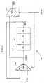
- a high-resolution graphics display accepts a live television signal from an analog television source.
- the television signal is decoded and digitized to a digital luminance/chrominance Y,C format by a digital television decoder 110.
- the decoded television signal is processed by an image window controller 100, and loaded into a high-resolution frame buffer 102 under the control of a frame buffer controller 104.
- the content of the frame buffer 102 is decoded to a red/green/blue representation by a digital television color matrix 106, to be shown on a monitor screen of the high-resolution display 108.
- the digital television decoder 110 also supplies a vertical synchronization signal VS, a horizontal synchronization signal, HS, a vertical blanking signal VB, a horizontal blanking signal HB, an odd/even field-specification signal ODDFLD and a sampling clock signal SCK.
- the frame-buffer controller 104 receives a request from the image window controller 100 to start loading data output from the image window controller 100 into the frame buffer 102 and also provides the image-window controller with the coordinates specifying the graphics window on the display screen.
- the image window controller 100 and its interface with the frame buffer 102 and the frame buffer controller 104 are described below.
- the digital television decoder 110 and the digital television color-matrix 106 which interfaces the frame buffer 102 with the monitor 108 are conventional and for conciseness will not be discussed in detail here.
- the image window controller 100 is adapted to receive luminance/chrominance digital data from the digital television decoder 110, process the data according to the image-scaling procedure described above, and transmit the resulting data to a data input of the frame buffer 102.
- a luminance data path 120 includes a luminance first-in-first-out ("FIFO") device 122.
- a chrominance data path 124 includes a chrominance first-in-first-out device 126 connected to a chrominance data register file 128.
- the luminance first-in-first-out device 122 temporarily stores the luminance data
- the chrominance first-in-first-out device 126 and the chrominance register file 128 store chrominance data.
- the first-in-first-out devices 122 and 126 can be implemented with three commercially-available integrated-circuit 4-bit-wide, 64-deep first-in-first-out memory units. For the case of image expansion in the vertical direction, greater storage capacity can be required for the first-in-first-out devices 122 and 126 as discussed below.
- Shift-in inputs 130,132 and shift-out inputs 134,136 of the first-in-first-out devices 122, 126, as well as the internal operations of the chrominance register file 128 are controlled by a horizontal window control unit 138.
- the horizontal window control unit 138 also provides a horizontal sampling request signal HSRQ, which corresponds to the television window horizontal timing coordinates.
- a vertical window control unit 140 is adapted to generate a vertical sampling request signal VSRQ that corresponds to vertical timing coordinates of the television window.
- the horizontal sampling request signal HSRQ and the vertical sampling request signal VSRQ are combined by a sampling-request gate 142 to produce the sampling-request signal SRQ.
- the sampling-request signal SRQ informs the frame-buffer controller 104 to start loading luminance output data and chrominance output data from the output of the image window controller 100 into the frame buffer 102.
- the timing coordinates of the television window are defined by internal counters of a synchronizer/generator 144.
- a vertical-count VCNT output is produced by counting television lines inside the television field; that is, by counting horizontal synchronization pulses HS in the range between the vertical synchronization pulses VS.
- a horizontal count HCNT is a number of sampling clock periods SCK inside a television line, i.e., between horizontal synchronization pulses HS.
- An oddfield signal which is active only during odd television-line fields of the television frames may be considered as an upper bit of the television line number, because its combination with the vertical count data VCNT provides a television line number inside the television frame.
- the frame-buffer-controller 104 After receiving the sampling-request signal SRQ, the frame-buffer-controller 104 generates a frame-buffer address FBAD sequence together with three control strobes RAS, CAS, TRQE and a frame-buffer write-enable signal FBWE.
- the frame buffer is built using video-dynamic RAM technology such as integrated circuits commercially available under the trade designation "TMX44C251 1Mbit VideoRAM" from Texas Instruments Incorporated of Carrolton, Texas. A description of the control signals for the video dynamic RAM integrated circuits is available in the manufacturer's data sheets.
- the frame-buffer controller 104 also supplies horizontal frame-buffer address HFBAD and vertical frame-buffer address VFBAD signals to the horizontal window control unit 138 and the vertical window control unit 140 to be used as coordinates of the pixels inside the graphics window. It also delivers the frame-buffer write-enable FBWE signal to the horizontal window control unit 138 to be used as a frame-buffer sampling clock reference.
- a host workstation provides the necessary control data to the image-window controller 100 and the frame-buffer controller 104 through host address and data buses under control of a host write enable signal HWE.
- the decoding of the addresses of different control registers and setup of different mode registers is done by an address decoder/mode-configuration unit 150, discussed below.
- the address-decoder/mode-configuration unit 150 is shown in Fig. 6. It includes a host address decoder 151, five AND gates 152-156, and a pattern-loading-mode flip/flop 157 and a jitter mode flip/flop 158.
- the pattern-loading mode flip/flop 157 generates a pattern-loading mode signal LSMOD.
- LSMOD pattern-loading mode signal
- sampling patterns are calculated by the host workstation according to the scaling procedure set forth above and are loaded into the horizontal-contraction-control-pattern RAM 160, vertical-contraction-control-pattern RAM 162 and jitter-control RAM 164 during vertical blank intervals.
- the pattern-loading-mode signal LSMOD is changed by the host workstation to one, thus enabling the sampling of luminance/chrominance data into the frame buffer 102.
- the signals VRTRAMWE, HORRAMWE and JITRAMWE are used as corresponding write-enable signals to the three RAM storage units 160, 162, and 164, respectively.
- the jitter-mode flip/flop 158 enables or disables a jitter mode during sampling into the frame buffer 102 by means of a jitter-mode signal JITEN. Disabling the jitter mode permits processing power of the host workstation to be saved, for example, in the case of fast-moving images, where jitter introduction is less important than in the case of slow moving or static images. If the jitter mode is not required, the jitter-control RAM 164 is idle and does not require loading data from the host workstation.
- FIG. 7 A functional diagram of a portion of the horizontal window control unit 138 which is concerned with scaling down or image contraction is shown in Fig. 7. It also includes a part of the synchronizer generator 144 to explain the interface between timing circuitry and the horizontal window control unit 138.
- the horizontal window control unit 138 includes the horizontal-contraction-control-pattern RAM 160.
- the horizontal-contraction-control-pattern RAM 160 stores a sequence of zeroes and ones referred to as a horizontal image-contraction control pattern to control a luminance-shift-in signal designated YFSI which is supplied to the shift-in input 130 of the luminance first-in-first-out device 122.
- the length of the horizontal-image-contraction control pattern corresponds to the maximum number of luminance samples from the output of the digital television decoder 110. For example, if the digital television decoder 110 uses the Philips digital video signal processing chip set, the horizontal-image-contraction control pattern length is 720.
- the horizontal-image-contraction control pattern is calculated by the host workstation, combined in groups of 4 bits each, and loaded in the first 180 addresses of the horizontal-contraction-control pattern RAM 160, with the first location designated address O.
- the horizontal contraction pattern RAM 160 need not be larger than 256 4-bit words.
- the size of the horizontal-contraction control pattern RAM 160 must be increased to 512. Note also, that if the length of the television window is less than an active television line, the beginning and the end of the horizontal-scaling transfer sequence must be zeroes. Therefore, the horizontal-scaling transfer sequence stored in the horizontal-contraction control pattern RAM 160 provides not only the scaling information data, but also the horizontal position of the television window relative to the television screen as well.
- a horizontal counter 168 supplies the addresses to the horizontal-contraction control pattern RAM 160 at address inputs 170.
- the horizontal counter 168 is clocked by a sampling-clock divided-by-four signal SCK/4 from an output 172 of a sampling-clock-divider counter 174.
- the sampling-clock-divider counter divides the sampling-clock signal by four.
- Both the horizontal counter 168 and the sample-clock-divider counter 174 are cleared by the horizontal blank signal HB from the digital television decoder 110 which is off during the time a horizontal line is active.
- the horizontal counter 168 starts counting immediately at the beginning of the active part of each television line and marks each group of four television samples by a consecutive number.
- the pattern-loading-mode signal LSMOD set by the host workstation disables the HB signal applied to the reset input of the horizontal counter 168 through an AND gate 176 and switches by means of a two-input single-line multiplexor 178 the clock input of the horizontal counter 168 to a horizontal-RAM-write-enable signal HORRAMWE from the AND gate 153 in the address-decoder/mode-configuration unit 150. Data from a data bus of the host workstation is loaded into the horizontal-contraction-control pattern RAM 160.
- the horizontal-RAM-write-enable signal HORRAMWE increments the horizontal counter 168 after each load, thus providing the next address for the horizontal-contraction-control-pattern RAM 160 to be loaded.
- the pattern-loading-mode signal LSMOD may be set back to 1 in order to restore the sampling-clock divided by four signal SCK/4 and the horizontal-blanking signal HB to the horizontal counter 168.
- the serial-out output 182 of the image-contraction shift register 180 is connected to a D input 183 of a type-D horizontal-sampling request flip/flop 184.
- the first "one" signal from the serial-out output 182 loads the flip/flop 184.
- a "Q" output 186 of the horizontal-sampling request flip/flop 184 generates the horizontal-sampling request signal HSRQ.
- the horizontal-sampling request signal will be active until the next horizontal synchronization signal HS, which is sufficient to store all the television active-line data sequence into the frame buffer 102.
- the horizontal-scaling bit signal appears on an output of a two-input/single-line multiplexor 190. If the horizontal-scaling-bit signal is 1, an OR gate 192 generates the luminance-shift-in clock signal YFSI, which shifts a luminance data sample to the luminance first-in-first-out device 122. If the horizontal-scaling-bit signal is O, the YFSI signal is not generated, and the luminance data sample is not loaded into the luminance first-in-first-out device 122, in other words, the luminance sample is skipped.
- the output of the multiplexor 190 is also connected to an increment input 194 of an image-contraction 3-bit up/down counter 196.
- An upper-bit output 198 of the image-contraction up/down counter 196 is clocked into a chrominance-pattern flip/flop 200.
- the output of the chrominance-pattern flip/flop 200 controls a chrominance-shift gate 202, which provides a sequence of chrominance-shift-in signals CFSI to the chrominance first-in-first-out device 126.
- the output of the chrominance-pattern flip/flop 200 is also connected to the decrement input 204 of the image-contraction up/down counter 196.
- the function of the image-contraction up/down counter 196 is to calculate the difference between the number of luminance samples and the number of chrominance samples written in the frame buffer 102 at any particular moment. More specifically, the image-contraction up/down counter 196 is incremented by one by each sampling-enable bit from the serial-out output 182 of the shift register 180 if the output of the chrominance pattern flip/flop 200 is zero so that chrominance sampling is disabled; the image-contraction up/down counter 196 is decremented if the output of the chrominance pattern flip-flop 200 is one so that chrominance sampling is enabled, but luminance sampling is disabled; it is in a hold state, when luminance and chrominance data sampling are both disabled or enabled.
- the difference between the number of luminance and chrominance samples loaded into the frame buffer 102 is more than four, and if the sampling-clock-divided-by-four signal SCK/4 from the sampling-clock divide counter 174 is in an active transition state, the upper bit of the image-contraction up/down counter 196 becomes 1 and the next sampling-clock pulse SCK loads 1 into the chrominance pattern flip/flop 200. As a result, four consecutive chrominance-shift-in pulses CFSI are issued, and four chrominance data samples are loaded into the chrominance first-in-first-out device 126 starting on a four horizontal sample boundary.
- the number of 4-bit words which can be stored into the horizontal-expansion-control-pattern RAM 220 corresponds to the horizontal size of the graphics image. Specifically, it is greater than or equal to the number of pixels in a horizontal line of high-resolution display screen divided by four.
Landscapes
- Engineering & Computer Science (AREA)
- Physics & Mathematics (AREA)
- Computer Hardware Design (AREA)
- General Physics & Mathematics (AREA)
- Theoretical Computer Science (AREA)
- Multimedia (AREA)
- Signal Processing (AREA)
- Controls And Circuits For Display Device (AREA)
- Color Television Systems (AREA)
- Processing Of Color Television Signals (AREA)
Applications Claiming Priority (2)
| Application Number | Priority Date | Filing Date | Title |
|---|---|---|---|
| US31499889A | 1989-02-24 | 1989-02-24 | |
| US314998 | 1999-05-20 |
Publications (3)
| Publication Number | Publication Date |
|---|---|
| EP0384419A2 true EP0384419A2 (de) | 1990-08-29 |
| EP0384419A3 EP0384419A3 (de) | 1992-05-27 |
| EP0384419B1 EP0384419B1 (de) | 1995-07-12 |
Family
ID=23222419
Family Applications (1)
| Application Number | Title | Priority Date | Filing Date |
|---|---|---|---|
| EP19900103282 Expired - Lifetime EP0384419B1 (de) | 1989-02-24 | 1990-02-21 | Farbfernsehbildfenster für ein Videoanzeigegerät |
Country Status (3)
| Country | Link |
|---|---|
| EP (1) | EP0384419B1 (de) |
| JP (1) | JPH02250585A (de) |
| DE (1) | DE69020753T2 (de) |
Cited By (18)
| Publication number | Priority date | Publication date | Assignee | Title |
|---|---|---|---|---|
| EP0493920A1 (de) * | 1990-12-21 | 1992-07-08 | Sun Microsystems, Inc. | Verfahren und Vorrichtung zum direkten Schreiben in einem Rasterpufferspeicher eines Rechners mit einem Fenstersystem, das den Bildschirm steuert |
| EP0572024A3 (de) * | 1992-05-27 | 1994-04-13 | Toshiba Kk | |
| WO1994007328A3 (en) * | 1992-09-15 | 1994-06-09 | Digital Pictures Inc | Digital video editing system and method |
| EP0610829A1 (de) * | 1993-02-05 | 1994-08-17 | Brooktree Corporation | Vorrichtung und Verfahren zur Anzeige von Informationen aus einem grafischen Speicher und einem Videospeicher auf einem Anzeigegerät |
| EP0653742A3 (de) * | 1993-11-12 | 1995-09-06 | Ibm | Vorrichtung zur Echtzeitskalierung von Bildern in einem Multimedien Arbeitsplatz. |
| EP0694189A4 (de) * | 1993-04-16 | 1997-01-15 | Data Translation Inc | Unterabgetastete video-bildwiedergabe auf einem rechnerbildschirm |
| US5719511A (en) * | 1996-01-31 | 1998-02-17 | Sigma Designs, Inc. | Circuit for generating an output signal synchronized to an input signal |
| US5790881A (en) * | 1995-02-07 | 1998-08-04 | Sigma Designs, Inc. | Computer system including coprocessor devices simulating memory interfaces |
| US5797029A (en) * | 1994-03-30 | 1998-08-18 | Sigma Designs, Inc. | Sound board emulation using digital signal processor using data word to determine which operation to perform and writing the result into read communication area |
| US5818468A (en) * | 1996-06-04 | 1998-10-06 | Sigma Designs, Inc. | Decoding video signals at high speed using a memory buffer |
| US5821947A (en) * | 1992-11-10 | 1998-10-13 | Sigma Designs, Inc. | Mixing of computer graphics and animation sequences |
| EP0840276A3 (de) * | 1996-11-01 | 1999-06-23 | Texas Instruments Incorporated | Fensterverarbeitung in einem Bildschirmanzeigensystem |
| EP0840277A3 (de) * | 1996-11-01 | 1999-06-23 | Texas Instruments Incorporated | Fensterverarbeitung in einem Bildschirmanzeigesystem |
| US6084909A (en) * | 1994-03-30 | 2000-07-04 | Sigma Designs, Inc. | Method of encoding a stream of motion picture data |
| US6124897A (en) * | 1996-09-30 | 2000-09-26 | Sigma Designs, Inc. | Method and apparatus for automatic calibration of analog video chromakey mixer |
| US6128726A (en) * | 1996-06-04 | 2000-10-03 | Sigma Designs, Inc. | Accurate high speed digital signal processor |
| US6421096B1 (en) | 1994-06-28 | 2002-07-16 | Sigman Designs, Inc. | Analog video chromakey mixer |
| US6452641B1 (en) | 1996-11-01 | 2002-09-17 | Texas Instruments Incorporated | Method and apparatus for providing and on-screen display with variable resolution capability |
Families Citing this family (1)
| Publication number | Priority date | Publication date | Assignee | Title |
|---|---|---|---|---|
| JP2010186194A (ja) * | 2010-04-09 | 2010-08-26 | Seiko Epson Corp | 画像処理装置 |
-
1990
- 1990-02-21 DE DE1990620753 patent/DE69020753T2/de not_active Expired - Lifetime
- 1990-02-21 EP EP19900103282 patent/EP0384419B1/de not_active Expired - Lifetime
- 1990-02-23 JP JP2041387A patent/JPH02250585A/ja active Granted
Cited By (22)
| Publication number | Priority date | Publication date | Assignee | Title |
|---|---|---|---|---|
| EP0493920A1 (de) * | 1990-12-21 | 1992-07-08 | Sun Microsystems, Inc. | Verfahren und Vorrichtung zum direkten Schreiben in einem Rasterpufferspeicher eines Rechners mit einem Fenstersystem, das den Bildschirm steuert |
| US5388200A (en) * | 1990-12-21 | 1995-02-07 | Sun Microsystems, Inc. | Method and apparatus for writing directly to a frame buffer |
| EP0572024A3 (de) * | 1992-05-27 | 1994-04-13 | Toshiba Kk | |
| WO1994007328A3 (en) * | 1992-09-15 | 1994-06-09 | Digital Pictures Inc | Digital video editing system and method |
| US5821947A (en) * | 1992-11-10 | 1998-10-13 | Sigma Designs, Inc. | Mixing of computer graphics and animation sequences |
| EP0610829A1 (de) * | 1993-02-05 | 1994-08-17 | Brooktree Corporation | Vorrichtung und Verfahren zur Anzeige von Informationen aus einem grafischen Speicher und einem Videospeicher auf einem Anzeigegerät |
| US5406306A (en) * | 1993-02-05 | 1995-04-11 | Brooktree Corporation | System for, and method of displaying information from a graphics memory and a video memory on a display monitor |
| US5706451A (en) * | 1993-04-16 | 1998-01-06 | Media 100 Inc. | Displaying a subsampled video image on a computer display |
| EP0694189A4 (de) * | 1993-04-16 | 1997-01-15 | Data Translation Inc | Unterabgetastete video-bildwiedergabe auf einem rechnerbildschirm |
| US5517612A (en) * | 1993-11-12 | 1996-05-14 | International Business Machines Corporation | Device for scaling real-time image frames in multi-media workstations |
| EP0653742A3 (de) * | 1993-11-12 | 1995-09-06 | Ibm | Vorrichtung zur Echtzeitskalierung von Bildern in einem Multimedien Arbeitsplatz. |
| US6084909A (en) * | 1994-03-30 | 2000-07-04 | Sigma Designs, Inc. | Method of encoding a stream of motion picture data |
| US5797029A (en) * | 1994-03-30 | 1998-08-18 | Sigma Designs, Inc. | Sound board emulation using digital signal processor using data word to determine which operation to perform and writing the result into read communication area |
| US6421096B1 (en) | 1994-06-28 | 2002-07-16 | Sigman Designs, Inc. | Analog video chromakey mixer |
| US5790881A (en) * | 1995-02-07 | 1998-08-04 | Sigma Designs, Inc. | Computer system including coprocessor devices simulating memory interfaces |
| US5719511A (en) * | 1996-01-31 | 1998-02-17 | Sigma Designs, Inc. | Circuit for generating an output signal synchronized to an input signal |
| US6128726A (en) * | 1996-06-04 | 2000-10-03 | Sigma Designs, Inc. | Accurate high speed digital signal processor |
| US5818468A (en) * | 1996-06-04 | 1998-10-06 | Sigma Designs, Inc. | Decoding video signals at high speed using a memory buffer |
| US6124897A (en) * | 1996-09-30 | 2000-09-26 | Sigma Designs, Inc. | Method and apparatus for automatic calibration of analog video chromakey mixer |
| EP0840277A3 (de) * | 1996-11-01 | 1999-06-23 | Texas Instruments Incorporated | Fensterverarbeitung in einem Bildschirmanzeigesystem |
| EP0840276A3 (de) * | 1996-11-01 | 1999-06-23 | Texas Instruments Incorporated | Fensterverarbeitung in einem Bildschirmanzeigensystem |
| US6452641B1 (en) | 1996-11-01 | 2002-09-17 | Texas Instruments Incorporated | Method and apparatus for providing and on-screen display with variable resolution capability |
Also Published As
| Publication number | Publication date |
|---|---|
| JPH02250585A (ja) | 1990-10-08 |
| DE69020753T2 (de) | 1996-03-14 |
| EP0384419B1 (de) | 1995-07-12 |
| EP0384419A3 (de) | 1992-05-27 |
| DE69020753D1 (de) | 1995-08-17 |
| JPH0432593B2 (de) | 1992-05-29 |
Similar Documents
| Publication | Publication Date | Title |
|---|---|---|
| US5283561A (en) | Color television window for a video display unit | |
| EP0384419B1 (de) | Farbfernsehbildfenster für ein Videoanzeigegerät | |
| US5559954A (en) | Method & apparatus for displaying pixels from a multi-format frame buffer | |
| JP2656737B2 (ja) | ビデオ情報を処理するためのデータ処理装置 | |
| US5896140A (en) | Method and apparatus for simultaneously displaying graphics and video data on a computer display | |
| EP0431845B1 (de) | Umwandlung von Videosignalen | |
| US5973746A (en) | Image data conversion processing device and information processing device having the same | |
| EP0462396B1 (de) | Dreifacher Halbbildpuffer für Fernsehbildspeicherung und Anzeige auf graphischen Rasterdarstellungsgerät | |
| US7236648B2 (en) | Scaling images for display | |
| US6172669B1 (en) | Method and apparatus for translation and storage of multiple data formats in a display system | |
| EP0139932B1 (de) | Einrichtung zur Abbildung eines Cursors | |
| US6356314B1 (en) | Image synthesizing device and image conversion device for synthesizing and displaying an NTSC or other interlaced image in any region of a VCA or other non-interlaced image | |
| JPH0695273B2 (ja) | デイスプレイ制御装置 | |
| USRE37879E1 (en) | Image control device for use in a video multiplexing system for superimposition of scalable video data streams upon a background video data stream | |
| JPH09149334A (ja) | ビデオ拡大装置 | |
| US7542098B2 (en) | Display device and display method | |
| US6023262A (en) | Method and apparatus in a computer system to generate a downscaled video image for display on a television system | |
| US5444497A (en) | Apparatus and method of transferring video data of a moving picture | |
| US5448264A (en) | Method and apparatus for separate window clipping and display mode planes in a graphics frame buffer | |
| US5148292A (en) | Apparatus for effectively compressing video data representing a relatively simple image having strong area correlation | |
| US5815143A (en) | Video picture display device and method for controlling video picture display | |
| US4506298A (en) | Method and apparatus for displaying objects on an interlaced raster scan television screen | |
| EP0593012B1 (de) | Videobilderanzeigevorrichtung und Verfahren zum Steuern einer Videobilderanzeige | |
| JP3484763B2 (ja) | 映像データ転送装置およびコンピュータシステム | |
| US5235429A (en) | Display apparatus having bandwidth reduction and vertical interpolation |
Legal Events
| Date | Code | Title | Description |
|---|---|---|---|
| PUAI | Public reference made under article 153(3) epc to a published international application that has entered the european phase |
Free format text: ORIGINAL CODE: 0009012 |
|
| AK | Designated contracting states |
Kind code of ref document: A2 Designated state(s): DE FR GB |
|
| 17P | Request for examination filed |
Effective date: 19901210 |
|
| PUAL | Search report despatched |
Free format text: ORIGINAL CODE: 0009013 |
|
| AK | Designated contracting states |
Kind code of ref document: A3 Designated state(s): DE FR GB |
|
| 17Q | First examination report despatched |
Effective date: 19940203 |
|
| GRAA | (expected) grant |
Free format text: ORIGINAL CODE: 0009210 |
|
| AK | Designated contracting states |
Kind code of ref document: B1 Designated state(s): DE FR GB |
|
| REF | Corresponds to: |
Ref document number: 69020753 Country of ref document: DE Date of ref document: 19950817 |
|
| ET | Fr: translation filed | ||
| PLBE | No opposition filed within time limit |
Free format text: ORIGINAL CODE: 0009261 |
|
| STAA | Information on the status of an ep patent application or granted ep patent |
Free format text: STATUS: NO OPPOSITION FILED WITHIN TIME LIMIT |
|
| 26N | No opposition filed | ||
| REG | Reference to a national code |
Ref country code: GB Ref legal event code: IF02 |
|
| PGFP | Annual fee paid to national office [announced via postgrant information from national office to epo] |
Ref country code: GB Payment date: 20090227 Year of fee payment: 20 |
|
| PGFP | Annual fee paid to national office [announced via postgrant information from national office to epo] |
Ref country code: DE Payment date: 20090331 Year of fee payment: 20 |
|
| PGFP | Annual fee paid to national office [announced via postgrant information from national office to epo] |
Ref country code: FR Payment date: 20090217 Year of fee payment: 20 |
|
| REG | Reference to a national code |
Ref country code: GB Ref legal event code: PE20 Expiry date: 20100220 |
|
| PG25 | Lapsed in a contracting state [announced via postgrant information from national office to epo] |
Ref country code: GB Free format text: LAPSE BECAUSE OF EXPIRATION OF PROTECTION Effective date: 20100220 |
|
| PG25 | Lapsed in a contracting state [announced via postgrant information from national office to epo] |
Ref country code: DE Free format text: LAPSE BECAUSE OF EXPIRATION OF PROTECTION Effective date: 20100221 |