EP0385421A2 - Appareil pour traitement d'images - Google Patents
Appareil pour traitement d'images Download PDFInfo
- Publication number
- EP0385421A2 EP0385421A2 EP90103868A EP90103868A EP0385421A2 EP 0385421 A2 EP0385421 A2 EP 0385421A2 EP 90103868 A EP90103868 A EP 90103868A EP 90103868 A EP90103868 A EP 90103868A EP 0385421 A2 EP0385421 A2 EP 0385421A2
- Authority
- EP
- European Patent Office
- Prior art keywords
- signal
- image
- maximum
- threshold
- character
- Prior art date
- Legal status (The legal status is an assumption and is not a legal conclusion. Google has not performed a legal analysis and makes no representation as to the accuracy of the status listed.)
- Withdrawn
Links
Images


Classifications
-
- H—ELECTRICITY
- H04—ELECTRIC COMMUNICATION TECHNIQUE
- H04N—PICTORIAL COMMUNICATION, e.g. TELEVISION
- H04N1/00—Scanning, transmission or reproduction of documents or the like, e.g. facsimile transmission; Details thereof
- H04N1/40—Picture signal circuits
- H04N1/40062—Discrimination between different image types, e.g. two-tone, continuous tone
Definitions
- the present invention relates to an image processing apparatus for processing a document image including characters and a photograph.
- image information with contrast e.g., characters and graphical patterns
- image information having tone e.g., a photograph
- a half-tone method such as a dither method.
- the read image information is simply subjected to gradation processing by an ordered dither method, the image quality of the area of the photograph is not deteriorated because gradation in this area is preserved, whereas the image quality of the area of character and graphical patterns is deteriorated because resolution in this area is deteriorated.
- a document image including three different types of image area is deemed to be processed in the field of OA (Office Automation).
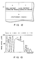
- a document D having an area of character and graphical patterns with contrast (to be referred to as a high contrast character section hereinafter), i.e., a section A, a photographic area having a moderate density gradient (to be referred to as a photograph section hereinafter), i.e., a section B, and an area of thin characters (to be referred to as a low contrast character section hereinafter), i.e., a section C.
- Typical image signal levels obtained by reading the document D having the sections A, B, and C are shown in Fig. 13.
- a difference between the maximum and minimum image signal levels is large in the high contrast character section A, a difference in the photograph section B is small, and an image signal level in the low contrast character section C falls within the range between the image signal levels of the sections A and B.
- the high and low contrast character sections are represented by a character section.
- the following method is proposed as a method of separating the above three image sections and simultaneously preserving the resolution and gradation. That is, a maximum density difference " ⁇ Dmax/Da" normalized by a mean density obtained by a maximum density difference ⁇ Dmax and a mean density Da of an image density in a local section within the image plane is obtained. This calculated value is compared with an estimating threshold value to separate an image into a character section and a photograph section, and the binary quantization methods are switched in accordance with the characteristics of the image sections.
- the "density” represents a signal level of an image read by a scanner and is different from the general "optical density”.
- the term “density” is used as the image signal level below, unless otherwise specified.
- the conventional method cannot accurately separate an image including of the high contrast character section A, the photograph section B, and the low contrast character section C into picture sections, and cannot simultaneously satisfy the requirements with respect to the resolution of the character section and the gradation of the photograph section. That is, adaptive processing cannot be performed in accordance with the image characteristics in units of sections.
- an image processing apparatus comprising a plurality of characteristic extracting circuits for extracting a plurality of characteristics from an image information signal, a decision circuit for estimating characteristics of the image information signal with reference to estimate data prepared in correspondence with characteristics of the image in accordance with the characteristics extracted by the plurality of characteristic extracting circuits, a first threshold generating circuit for generating a first threshold signal for binarizing the image information signal, a second threshold generating circuit for generating a second threshold signal for binarizing the image information signal, a selector circuit for selecting either the first or second threshold signal generated by either the first or second threshold generating circuit, and a binarizing circuit for binarizing the image information signal by using the first or second threshold signal selected by the selector circuit as a threshold signal.
- the estimate information are prepared from various pieces of document image information on the basis of statistical values of a plurality of characteristics, and the plurality of characteristics are extracted from the obtained image information signal.
- the extracted characteristics are supplied to the estimate circuit, and the decision circuit outputs an estimate signal corresponding to the image characteristics.
- the first or second threshold value is selected on the basis of the estimate signal, and the selected value serves as a threshold value for binarizing the image information signal.
- Fig. 1 is a block diagram showing a conceptual arrangement of an image processing apparatus according to the present invention.
- An image signal S1 (8 bits/pixel) read by a reader or scanner (not shown) is supplied to a line buffer 1.
- the line buffer 1 temporarily stores the image signal S1.
- the image signal S1 stored in the line buffer 1 is supplied as image data S2 to a discrimination circuit 2 in synchronism with a clock signal (not shown).
- the discrimination circuit 2 comprises a first characteristic extracting circuit 3, a second characteristic extracting circuit 4, and a decision circuit 5.
- the first characteristic extracting circuit 3 receives the image data S2 as its input and outputs a maximum density difference signal S3 (to be described in detail later) as a first characteristic signal.
- the second characteristic extracting circuit 4 receives the image data S2 as its input and outputs a mean density signal S4 (to be described in detail later) as a second characteristic signal.
- the decision circuit 5 which receives the maximum density difference signal S3 as the first characteristic signal and the mean density signal S4 as the second characteristic signal estimates that the image data S2 is a character or photograph in units of pixels and outputs a decision signal S5 as an estimation result to a selector 6.
- the selector 6 selects a first threshold signal Th1 output from a first threshold generating circuit 7 or a second threshold signal Th2 output from a second threshold generating circuit 8 in accordance with the estimate signal S5 and outputs the selected threshold value to a binary conversion circuit 9 as a threshold value Th for actually binary converting the image data.
- the binarization circuit 9 compares the threshold signal Th from the selector circuit 6 with an image signal S6 output from a delay circuit 10 for delaying the image data S2 by a predetermined period of time to estimate whether a pixel of the image signal S6 is a white or black pixel.
- the binarization circuit 9 outputs the image signal S6 as a binary image signal S7. More specifically, when the signal level of the image signal S6 output from the delay circuit 10 is higher than the threshold signal Th, the binarization circuit 9 outputs a signal "1" (e.g., this signal corresponds to the black pixel).
- the binarization circuit 9 outputs a signal "0" (e.g., this signal corresponds to a white pixel).
- the delay circuit 10 comprises, e.g., a delay memory for delaying the image data S2 by a period of time required for determining the binarization threshold value Th as the image data S2 is transmitted through the discrimination circuit 2, the selector 6, the first threshold generating circuit, and the like.
- the decision circuit 5 discriminates a character section from a photograph section in accordance with the maximum density difference signal S3 representing the maximum density difference ⁇ Dmax as the first characteristic and the mean density signal S4 representing the mean density within the window as the second characteristic.
- the decision circuit 5 comprises a 64-Kbit ROM which receives the maximum density difference signal S3 (the first characteristic) and the mean density signal S4 (the second characteristic) as address inputs.
- the decision circuit 5 estimates whether the input pixel is a character or photograph pixel and outputs the decision signal S5 as a decision result.
- This decision signal S5 has the following values: "1" for character pixel "0" for photograph pixel
- the dynamic threshold calculation circuit 7 serving as the first threshold generating circuit calculates a threshold value for processing a given pixel by a dynamic threshold value when the given pixel is decision as a character pixel.
- This binarization threshold value Bh is supplied to the selector 6 as the first threshold signal Th1.
- the second threshold generating circuit 8 determines a binarization threshold value for a photograph section and outputs this to the selector 6 as the second threshold signal Th2.
- a matrix for this threshold value is exemplified by a known 4 ⁇ 4 dither threshold matrix, as shown in Fig. 4.
- the selector 6 selects the first or second threshold signal Th1 or Th2 in accordance with the value of the decision signal S5 and outputs the selected signal as the threshold signal Th.
- the binarization circuit 9 compares the threshold signal Th thus determined with the image signal S6 delayed by the delay circuit 10 and outputs a binary-converted image signal S7.
- Fig. 5 is a detailed block diagram of the maximum/minimum value detection circuit 11.
- the image data S2 stored in the line buffer 1 are sequentially supplied to comparators 21, 22, 23, and 24 through a selector 20 in synchronism with a clock signal CLK in units of four pixels (8 bits/pixel).
- CLK clock signal
- a counter 27 comprises a 2-bit counter operated in response to the clock signal CLK and generates selection signals SE0 and SE1 for the selector 20.
- the selector 20 outputs the image data S2 supplied to input ports I3 to I0 to any set of output ports A3 to A0, B3 to B0, C3 to C0, and D3 to D0 in accordance with the selection signals SE1 and SE0 from the counter 27.
- the comparator 21 detects maximum and minimum densities 21a and 21b of the pixels of the (j-1)th column and supplies them to comparators 25 and 26, respectively.
- the comparator 22 detects maximum and minimum densities 22a and 22b of the pixels of the jth column and supplies them to the comparators 25 and 26, respectively.
- the comparator 23 detects maximum and minimum densities 23a and 23b of the pixels of the (j+1)th column and supplies them to the comparators 25 and 26, respectively.
- the comparator 24 detects maximum and minimum densities 24a and 24b of the pixels of the (j+2)th column and supplies them to the comparators 25 and 26, respectively.
- the comparator 25 receives the maximum density 21a of the (j-1)th column output from the comparator 21, the maximum density 22a of the jth column output from the comparator 22, the maximum density 23a of the (j+1)th column output from the comparator 23, and the maximum density 24a of the (j+2)th column output from the comparator 24, and detects a maximum density therefrom.
- the comparator 25 then outputs the maximum image density signal S8.
- the comparator 26 receives the minimum density 21b of the (j-1)th column output from the comparator 21, the minimum density 22b of the jth column output from the comparator 22, the minimum density 23b of the (j+1)th column output from the comparator 23, and the minimum density 24b of the (j+2)th column output from the comparator 24, and detects a minimum density therefrom.
- the comparator 26 then outputs the minimum image density signal S9.
- the maximum and minimum image density signals S8 and S9 are supplied to the subtractor 12.
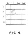
- a target pixel subjected to binary conversion is given by a pixel of the ith row and the jth column indicated by a hatched area.
- the window comprises 16 pixels of the (i-1)th row to the (i+2)th row and the (j-1)th column to the (j+2)th column.
- the data of the pixel of the (j-1)th column are supplied to the comparator 21, and the comparator 21 outputs the maximum and minimum densities 21a and 21b.
- data of pixels of the jth column and the (i-1)th to (i+2)th rows of the window are supplied to inputs I3 to I0 of the selector 20, respectively.
- the data of pixels of the jth column are supplied to the comparator 22, and the comparator 22 outputs the maximum and minimum densities 22a and 22b.
- data of pixels of the (j+1)th column and the (i-1)th to (i+2)th rows of the window are supplied to the inputs I3 to I0 of the selector 20, respectively.
- Data of the pixels of the (j+1)th column are supplied to the comparator 23, and the comparator 23 outputs the maximum and minimum densities 23a and 23b.
- the maximum densities 21a, 22a, 23a, and 24a of the (j-1)th, jth, (j+1)th, and (j+2)th columns are supplied to the comparator 25 and the minimum densities 21b, 22b, 23b, and 24b thereof are supplied to the comparator 26.
- the comparator 25 detects the maximum image density signal S8 of the window from the maximum densities 21a, 22a, 23a, and 24a of the respective columns
- the comparator 26 detects the minimum image density signal S9 of the window from the minimum densities 21b, 22b, 23b, and 24b of the respective columns.
- the maximum image density signal S8 detected by the comparator 25 an the minimum image density signal S9 detected by the comparator 26 are input to the subtractor 12.
- the subtractor 12 calculates and outputs the maximum density difference signal S3.
- the maximum density difference signal S3 is supplied to the decision circuit 5.
- the decision circuit 5 also receives the mean density signal S4 output from the mean value calculation circuit 4 (to be described in detail later).
- the estimation result is output to the selector 6 as the estimate signal S5.
- the mean value calculation circuit 4 will be described with reference to a block diagram of Fig. 8.
- Arrangements and functions of a selector 30 and a counter 37 are the same as those in the maximum/minimum value detection circuit 11, and a detailed description thereof will be omitted.
- the selector 20 outputs the image data S2 supplied to the inputs I3 to I0 to the output ports A3 to A0, B3 to B0, C3 to C0, or D3 to D0 in accordance with the selection signals SE0 and SE1 generated by the counter 37.
- the 16 pixels shown in Fig. 6 four pixels of the (j-1)th, jth, (j+1)th, and (j+2)th columns are output to adders 31, 32, 33, and 34, respectively.
- the adder 31 adds the densities of the pixels of the (j-1)th column
- the adder 32 adds the densities of the pixels of the jth column
- the adder 33 adds the densities of the pixels of the (j+1)th column
- the adder 34 adds the densities of the pixels of the (j+2)th column.
- the sums from the adders 31, 32, 33, and 34 are supplied to an adder 35.
- Each of the adders 31, 32, 33, and 34 adds 8-bit data and outputs 10-bit data.
- the adder 35 adds a density 31a of the (j-1)th column output from the adder 31, a density 32a of the jth column output from the adder 32, a maximum density 33a of the (j+1)th column output from the adder 33, and a density 34a of the (j+2)th column output from the adder 34 and outputs a total sum-of-density signal 35a.
- the adder 35 adds 10-bit data and outputs 12-bit data.
- the total sum-of-density signal 35a is supplied to a divider 36.
- a target window contains 16 pixels of the (i-1)th to (i+2)th rows and the (j-1)th to (j+2)th columns.
- data of the pixels of the jth column and the (i-1)th to (i+2)th rows of the window are supplied to the inputs I3 to I0 of the selector 20, respectively.
- Data of the pixels of the jth column are supplied to the adder 32, and the adder 32 outputs a sum-of-density signal 32a.
- data of pixels of the (j+1)th column and the (i-1)th to (i+2)th rows are supplied to the inputs I3 to I0 of the selector 20.
- Data of the pixels of the (j+1)th column are supplied to the adder 33, and the adder 33 outputs a sum-of-density signal 33a.
- data of the pixels of the (j+2)th column and the (i-1)th to (i+2)th rows are supplied to the inputs I3 to I0 of the selector 20.
- Data of the pixels of the (j+2)th column are supplied to the adder 34, and the adder 34 outputs a sum-of-density signal 34a.
- the sum-of-density signals 31a, 32a, 33a, and 34a of the (j-1)th, jth, (j+1)th, and (j+2)th columns of the target window are obtained and output.
- the sum-of-density signals 31a, 32a, 33a, and 34a of the (j-1)th, jth, (j+1)th, and (j+2)th columns of the window are supplied to the adder 35.
- the adder 35 calculates a total sum of of the densities of the window from the sum-of-density signals 31a, 32a, 33a, and 34a of the respective columns and outputs the total sum-of-density signal 35a.
- the total sum-of-density signal 35a calculated by the adder 35 is supplied to a divider 36.
- the mean density signal S4 is supplied to the decision circuit 5.
- the decision circuit 5 receives the maximum density difference signal S3 output from the mean value calculation circuit 4.
- the estimation result is output to the selector circuit 6 as the discrimination signal S5.
- the estimate circuit 5 discriminates a character section from a photograph section on the basis of the an estimation condition in accordance with the maximum density difference signal S3 and the mean density signal S4.
- the above discrimination is performed by using the ROM shown in Fig. 3, as previously described. That is, a 16-bit signal as a sum of the maximum density difference signal S3 and the mean density signal S4 is supplied to the ROM as address data, and the image signal is discriminated as a character or photograph section in accordance with a correlation between the maximum density difference signal S3 and the mean density signal S4.
- the discrimination signal S5 is output from the estimate circuit 5.
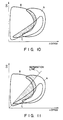
- Fig. 10 shows the correlation between the maximum density difference ⁇ Dmax and the mean density Da obtained from various pieces of document image information.
- a section A is a high contrast character section
- a section B is a photograph section
- a section C is a low contrast character section.
- Each characteristic is represented by 8-bit data.
- a hatched portion represents a discrimination error section but has a narrow distribution of occurrence probability (not shown), and image quality is rarely deteriorated. Therefore, even if the hatched portion is determined to be a character or photograph section, the hatched portion rarely adversely affects the image quality.
- Fig. 11 shows a conventional discrimination method using the normalized maximum density difference as a characteristic. It is apparent from Fig. 11 that the area of the hatched portion representing discrimination errors is increased. A separation line has different gradients corresponding to different estimate threshold values. Even if all cases are assumed, the area of the discrimination errors is apparently increased as compared with the case of Fig. 10. Since an area where an occurrence probability (not shown) is large is defined as the area of the discrimination errors, the image quality is greatly deteriorated by the conventional method.
- the decision circuit 5 receives the maximum density difference signal S3 representing the maximum density difference ⁇ Dmax and the mean density difference signal S4 representing the mean density Da.
- decision data representing whether the input image signal represents a character or photograph section is created in accordance with a distribution pattern of the maximum density difference ⁇ Dmax and the mean density Da of the character and photograph sections obtained by the statistical values of the document images.
- the decision data is stored in a ROM in the decision circuit 5, and the decision data is read out from the ROM by address data having of the maximum density difference signal S3 and the mean density signal S4, thereby discriminating a character section from a photograph section. Therefore, a highly accurate estimation result can be obtained.
- decision information prepared on the basis of statistical values of a plurality of characteristics from various pieces of document image information is prepared in the decision circuit 5, and characteristics are extracted from the first and second characteristic extracting circuits 3 and 4 on the basis of the obtained image information signal.
- the extracted characteristic signals are supplied to the decision circuit 5, and the decision signal S5 corresponding to the characteristic of the image is obtained from the decision circuit 5.
- the first or second threshold value Th1 or Th2 is selected on the basis of the discrimination signal S5.
- the selected threshold value is used as the threshold value Th for binary conversion. Therefore, the image information can be separated into sections corresponding to the characteristics of the image, and binary conversion suitable for the characteristic of the image in each section can be performed.
- the size of the reference section (window) is not limited to the 4 (pixel) ⁇ 4 (pixel) window.
- the size of the window may be arbitrarily changed.
- decision is performed in units of pixels.
- discrimination may be performed in units of blocks each including of N (pixels) (N is an integer of 2 or more) ⁇ N (pixels). In this case, the processing speed can be increased, and a high-speed image processing apparatus can be obtained.
- Difference values may be selected as the threshold value Bh in dynamic threshold processing.
- a dither threshold distribution need not be limited to a dot distributed distribution, but may be, e.g., a dot concentrated distribution.
- a nonlinear threshold distribution corresponding to output characteristics of an output unit may be obtained. Therefore, optimal gradation expressions can be obtained to cope with different types of printer, such as a laser printer, a thermal transfer printer, and an ink-jet printer.
- the characteristic values and decision threshold values are calculated on the basis of a value corresponding to the image signal read by the reader, i.e., corresponding to the reflectance of image information.
- this value may be converted into an image density (i.e., a logarithmic value of a reciprocal number of the reflectance), or decision may be performed on the basis of a signal converted in consideration of human visual characteristics.
- decision is performed with reference to a two-dimensional table using two different characteristics.
- decision may be performed by a multi-dimensional table using three or more characteristics.
- the number of quantization bits of each characteristic signal may be increased to improve decision precision.
Landscapes
- Engineering & Computer Science (AREA)
- Multimedia (AREA)
- Signal Processing (AREA)
- Facsimile Image Signal Circuits (AREA)
- Image Input (AREA)
- Character Input (AREA)
Applications Claiming Priority (2)
| Application Number | Priority Date | Filing Date | Title |
|---|---|---|---|
| JP1050391A JPH02228878A (ja) | 1989-03-02 | 1989-03-02 | 画像処理装置 |
| JP50391/89 | 1989-03-02 |
Publications (2)
| Publication Number | Publication Date |
|---|---|
| EP0385421A2 true EP0385421A2 (fr) | 1990-09-05 |
| EP0385421A3 EP0385421A3 (fr) | 1990-11-07 |
Family
ID=12857574
Family Applications (1)
| Application Number | Title | Priority Date | Filing Date |
|---|---|---|---|
| EP19900103868 Withdrawn EP0385421A3 (fr) | 1989-03-02 | 1990-02-28 | Appareil pour traitement d'images |
Country Status (2)
| Country | Link |
|---|---|
| EP (1) | EP0385421A3 (fr) |
| JP (1) | JPH02228878A (fr) |
Cited By (2)
| Publication number | Priority date | Publication date | Assignee | Title |
|---|---|---|---|---|
| EP0488534A3 (en) * | 1990-11-26 | 1992-11-25 | Canon Kabushiki Kaisha | Outputting method and apparatus |
| US5408592A (en) * | 1991-03-20 | 1995-04-18 | Brother Kogyo Kabushiki Kaisha | Printer having a data output time controller |
Families Citing this family (4)
| Publication number | Priority date | Publication date | Assignee | Title |
|---|---|---|---|---|
| AU596758B2 (en) * | 1987-11-13 | 1990-05-10 | Jp Steel Plantech Co. | Metal-making apparatus involving the smelting reduction of metallic oxides |
| JP2936766B2 (ja) * | 1991-01-31 | 1999-08-23 | 日本電気株式会社 | 画像入力装置 |
| US7227988B2 (en) * | 2002-07-01 | 2007-06-05 | Xerox Corporation | Prioritized PDL segmentation producing two bit selector |
| TWI366156B (en) * | 2003-07-01 | 2012-06-11 | Xerox Corp | Method and system for thinning or eroding a gray image of an input image defined by a plurality of pixels |
Family Cites Families (4)
| Publication number | Priority date | Publication date | Assignee | Title |
|---|---|---|---|---|
| GB2129652B (en) * | 1982-10-27 | 1986-06-04 | Matsushita Electric Industrial Co Ltd | Method and apparatus for processing image signal |
| US4783838A (en) * | 1984-12-26 | 1988-11-08 | Konishiroku Photo Industry Co., Ltd. | Image processing method and apparatus therefor |
| US4668995A (en) * | 1985-04-12 | 1987-05-26 | International Business Machines Corporation | System for reproducing mixed images |
| JPS62100077A (ja) * | 1985-10-28 | 1987-05-09 | Nippon Telegr & Teleph Corp <Ntt> | 符号化方法および装置 |
-
1989
- 1989-03-02 JP JP1050391A patent/JPH02228878A/ja active Pending
-
1990
- 1990-02-28 EP EP19900103868 patent/EP0385421A3/fr not_active Withdrawn
Cited By (3)
| Publication number | Priority date | Publication date | Assignee | Title |
|---|---|---|---|---|
| EP0488534A3 (en) * | 1990-11-26 | 1992-11-25 | Canon Kabushiki Kaisha | Outputting method and apparatus |
| US5740339A (en) * | 1990-11-26 | 1998-04-14 | Canon Kabushiki Kaisha | Outputting method and apparatus |
| US5408592A (en) * | 1991-03-20 | 1995-04-18 | Brother Kogyo Kabushiki Kaisha | Printer having a data output time controller |
Also Published As
| Publication number | Publication date |
|---|---|
| EP0385421A3 (fr) | 1990-11-07 |
| JPH02228878A (ja) | 1990-09-11 |
Similar Documents
| Publication | Publication Date | Title |
|---|---|---|
| US6201612B1 (en) | Image processing method and apparatus employing block error diffusion | |
| US4701807A (en) | Method and apparatus for processing an image | |
| US5109436A (en) | Image data processing system with adaptive binary quantization | |
| US4998122A (en) | Image binarization apparatus | |
| US4817174A (en) | Image processing apparatus | |
| US5278919A (en) | Image area determining apparatus | |
| EP0685959B1 (fr) | Appareil de traitement d'image pour identification de caratères, photo et d'images à points dans le domain d'une image | |
| EP0548571A1 (fr) | Système et méthode pour l'application d'un seuil adaptatif et bidirectionnel | |
| US5177795A (en) | Image processing apparatus | |
| JP3749282B2 (ja) | 画像処理装置 | |
| EP0297516B1 (fr) | Système rendant un signal d'image binaire | |
| EP0385421A2 (fr) | Appareil pour traitement d'images | |
| US4996602A (en) | Image-processing apparatus | |
| JP2815157B2 (ja) | 画像処理装置 | |
| US5299030A (en) | Image data processing method and apparatus with mixture of simple binarization and psuedo intermediate tone | |
| JP2874592B2 (ja) | 文字・写真・網点領域を判別する画像処理装置 | |
| JP3245600B2 (ja) | 画像処理装置 | |
| JPH0793534A (ja) | 画像処理装置 | |
| JPS63288565A (ja) | 画像処理装置 | |
| JPH0698157A (ja) | 中間調画像形成装置 | |
| JPS6359272A (ja) | 画像処理装置 | |
| JPH0267869A (ja) | 画像処理装置 | |
| JPH0326065A (ja) | 画像処理装置 | |
| JPH04189069A (ja) | 画像処理装置 | |
| JPH02132968A (ja) | 画像処理装置 |
Legal Events
| Date | Code | Title | Description |
|---|---|---|---|
| PUAI | Public reference made under article 153(3) epc to a published international application that has entered the european phase |
Free format text: ORIGINAL CODE: 0009012 |
|
| 17P | Request for examination filed |
Effective date: 19900323 |
|
| AK | Designated contracting states |
Kind code of ref document: A2 Designated state(s): DE FR GB |
|
| PUAL | Search report despatched |
Free format text: ORIGINAL CODE: 0009013 |
|
| AK | Designated contracting states |
Kind code of ref document: A3 Designated state(s): DE FR GB |
|
| RHK1 | Main classification (correction) |
Ipc: H04N 1/415 |
|
| 17Q | First examination report despatched |
Effective date: 19920908 |
|
| STAA | Information on the status of an ep patent application or granted ep patent |
Free format text: STATUS: THE APPLICATION IS DEEMED TO BE WITHDRAWN |
|
| 18D | Application deemed to be withdrawn |
Effective date: 19930629 |