EP0385470A2 - Circuit de commande pour laser à semi-conducteur - Google Patents
Circuit de commande pour laser à semi-conducteur Download PDFInfo
- Publication number
- EP0385470A2 EP0385470A2 EP90104011A EP90104011A EP0385470A2 EP 0385470 A2 EP0385470 A2 EP 0385470A2 EP 90104011 A EP90104011 A EP 90104011A EP 90104011 A EP90104011 A EP 90104011A EP 0385470 A2 EP0385470 A2 EP 0385470A2
- Authority
- EP
- European Patent Office
- Prior art keywords
- semiconductor laser
- transistors
- driving circuit
- current
- transistor group
- Prior art date
- Legal status (The legal status is an assumption and is not a legal conclusion. Google has not performed a legal analysis and makes no representation as to the accuracy of the status listed.)
- Granted
Links
Images


Classifications
-
- H—ELECTRICITY
- H03—ELECTRONIC CIRCUITRY
- H03K—PULSE TECHNIQUE
- H03K17/00—Electronic switching or gating, i.e. not by contact-making and –breaking
- H03K17/12—Modifications for increasing the maximum permissible switched current
-
- H—ELECTRICITY
- H01—ELECTRIC ELEMENTS
- H01S—DEVICES USING THE PROCESS OF LIGHT AMPLIFICATION BY STIMULATED EMISSION OF RADIATION [LASER] TO AMPLIFY OR GENERATE LIGHT; DEVICES USING STIMULATED EMISSION OF ELECTROMAGNETIC RADIATION IN WAVE RANGES OTHER THAN OPTICAL
- H01S5/00—Semiconductor lasers
- H01S5/04—Processes or apparatus for excitation, e.g. pumping, e.g. by electron beams
- H01S5/042—Electrical excitation ; Circuits therefor
- H01S5/0427—Electrical excitation ; Circuits therefor for applying modulation to the laser
-
- H—ELECTRICITY
- H01—ELECTRIC ELEMENTS
- H01S—DEVICES USING THE PROCESS OF LIGHT AMPLIFICATION BY STIMULATED EMISSION OF RADIATION [LASER] TO AMPLIFY OR GENERATE LIGHT; DEVICES USING STIMULATED EMISSION OF ELECTROMAGNETIC RADIATION IN WAVE RANGES OTHER THAN OPTICAL
- H01S5/00—Semiconductor lasers
- H01S5/04—Processes or apparatus for excitation, e.g. pumping, e.g. by electron beams
- H01S5/042—Electrical excitation ; Circuits therefor
- H01S5/0428—Electrical excitation ; Circuits therefor for applying pulses to the laser
-
- H—ELECTRICITY
- H01—ELECTRIC ELEMENTS
- H01S—DEVICES USING THE PROCESS OF LIGHT AMPLIFICATION BY STIMULATED EMISSION OF RADIATION [LASER] TO AMPLIFY OR GENERATE LIGHT; DEVICES USING STIMULATED EMISSION OF ELECTROMAGNETIC RADIATION IN WAVE RANGES OTHER THAN OPTICAL
- H01S5/00—Semiconductor lasers
- H01S5/06—Arrangements for controlling the laser output parameters, e.g. by operating on the active medium
- H01S5/062—Arrangements for controlling the laser output parameters, e.g. by operating on the active medium by varying the potential of the electrodes
- H01S5/06209—Arrangements for controlling the laser output parameters, e.g. by operating on the active medium by varying the potential of the electrodes in single-section lasers
Definitions
- the present invention relates to a semiconductor laser driving circuit and, more particularly, to a semiconductor laser driving circuit comprising an output circuit composed of a plurality of transistors connected in parallel and a current source.
- Semiconductor lasers used in light output circuits for optical communication during daytime require driving circuits which accommodate variations in values of components used and variations in temperature.
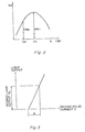
- Fig. 1 illustrates an example of a prior art semiconductor driving circuit.
- This circuit comprises a parallel circuit 2 having n (n>1) transistors Tr11 to Tr1n connected in parallel and a parallel circuit 20 having n transistors Tr21 to Tr2n connected in parallel.
- Circuits 2 and 20 together constitute a differential pair forming a differential amplifier.
- a common base input V1 of parallel circuit 2 and a common base input V2 of parallel circuit 20 are supplied with pulse signals of opposite polarities.
- transistors Tr11 to Tr1n are all turned on so that a semiconductor laser 1 is driven by a current source 3 to emit a desired light output pulse.
- the differential pair portion shown by broken lines in Fig. 1 is usually used in the form of an integrated circuit (refer to Japanese Unexamined Patent Publications Nos. 57-10279 and 63-119281).
- the number of transistors constituting parallel circuit 2 is pre selected such that a (rated) collector current is allowed to flow through each transistor, optimizing the characteristics of each transistor, i.e., which maximizes the current amplification factor hFE, like the collector current Ic1 shown in Fig. 2 when an allowable maximum current flowing through the semiconductor laser 1 is divided equally by transistors Tr11 to Tr1n.
- the driving pulse current Ip may be small and the driving pulse current Ip may have to be increased. This depends upon variations in the semiconductor laser 1 and variations in temperature. If the current Io of current source 3 is varied accordingly, the collector current flowing through each of the transistors will become, for example, Ic1 (where the current amplification factor has a maximum value of hFE1) or Ic2 (where the current amplification factor is hFE2 less than hFE1). These different collector currents Ic1 and Ic2 will result in different operating frequency characteristics, as shown in Fig. 4.
- a feature of the present invention resides in a semiconductor laser driving circuit comprising a current source for supplying a current to a semiconductor laser, a transistor group in which a plurality of transistors is disposed in parallel and a predetermined number of transistors selected from said transistor group being connected in parallel between said current source and said semiconductor laser; and wherein the number of transistors constituting said transistor group is set such that an equal collector current flows through each of the transistors, thus optimizing their operating characteristics when an allowable maximum current of said semiconductor laser is equally divided by all of the transistors in said transistor group, and the number of selected transistors is set such that a current is allowed to flow through said semiconductor laser, causing it to generate a required light output, and the optimum collector current flows through all of the selected transistors.
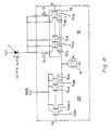
- the semiconductor laser driving circuit comprises a current source 3 for supplying a current to a semiconductor laser 1 and a transistor group 12 in which a plurality of transistors are connected in parallel.
- a predetermined number of transistors 14, connected in parallel and selected from the transistor group 12, are connected between the semiconductor laser 1 and the current source 3.
- the number of transistors forming the transistor group 12 is set such that, when an allowable maximum current flowing through the semiconductor laser 1 is equally divided by all the transistors of the transistor group 12, a collector current flows through each of the transistors which optimizes its characteristics (that is, the current amplification factor hFE has a maximum value).
- the number of transistors 14 to be selected from the transistor group 12 is set such that a current Ip for generating a required light output Po flows through the semiconductor laser 1 and the optimum collector current flows through each of the transistors 14.
- the present invention produces two main advantages.
- the driving pulse current Ip flows through the semiconductor laser 1, which causes the laser 1 to deliver the required light output Po (refer to Fig. 3), and the same optimum collector current always flows through each of a predetermined number of transistors 14 connected to the semiconductor laser 1. Therefore, the collector current of each transistor has an optimum fixed value, such as Ic1, as shown in Fig. 2, even if the driving pulse current Ip varies from sample to sample of a given type of semiconductor laser used. This prevents degradation of the high-speed response characteristics (rising and falling characteristics) of each of the transistors used.
- transistors 15 as well as the selected transistors 14 in the transistor group 12 are connected to the current source 3 so as to be supplied with the optimum collector current therefrom, stray capacitance can be eliminated from the transistors 15 and a driving circuit comprising the transistor group 12 can be used as one of a differential pair. This will allow the semiconductor laser to be driven with faster response characteristics.
- a semiconductor laser driving circuit comprises a differential pair composed of a transistor parallel circuit 20 as in the prior driving circuit shown in Fig. 1 and a transistor group 12 having the same number of transistors as the transistor parallel circuit 20.
- the current Io of the current source 3 is selected so as to accommodate the maximum value of the driving pulse current Ip, which is subject to variation due to manufacturing processes, of the semiconductor laser 1.
- Ico the optimum collector current for a transistor
- Io the current supplied by current source 3.
- the optimum driving pulse current Ip (refer to Fig. 3) for the semiconductor laser 1 is 2Io/n.
- two transistors Tr11 and Tr12 are connected in parallel between the semiconductor laser 1 and the current source 3.
- the other transistors Tr13 through Tr1n have their emitters connected to the current source 3 and their collectors connected to ground.
- the semiconductor laser 1 requires a driving pulse current of n x Io/n.
- the semiconductor laser 1 requires m x Io/n (m ⁇ n) as its optimum driving current Ip
- m transistors are arbitrarily selected from the transistor group 12 and connected between the semiconductor laser 1 and the current source 3.
- Figs. 7 and 8 are distinct from each other in the optimum driving pulse current Ip for the semiconductor laser 1. However, in both embodiments, the current flowing through each of the transistors in the transistor group 12 has a constant value of Io/n, independent of the magnitude of the driving pulse current for the semiconductor laser.
- the switching current flowing through the transistor group 12 always amount to Io, which is identical to that of the transistor parallel circuit 20, thus forming a differential pair with the transistor group.
- Io which is identical to that of the transistor parallel circuit 20, thus forming a differential pair with the transistor group.
- the driving circuit is formed of a differential pair.
- a differential pair configuration may not be needed so long as bipolar transistors are used.
- the transistors 15 as well as the transistors 14 connected to the semiconductor laser 1 are connected to ground. This is to allow the same current to flow through each of the transistors in transistor group 12 and transistor parallel circuit 20, which form the differential pair, and to eliminate stray capacitances and thereby achieve a high-speed response. Even where the transistors 15 are not supplied with current, degradation of waveforms is prevented.
- transistors constituting transistor group 12 have their emitters connected together and their bases connected together, their collector currents remain unchanged.
- suitable resistors may be connected between the transistors 15 and ground.
- another semiconductor laser 11 may be connected between the transistors 15 and ground as shown in Fig. 9. In this case, if the semiconductor lasers 1 and 11 have different characteristics, the number of transistors to be connected to them will vary according to these characteristics.
- the transistors 14 may be connected to semiconductor laser 1 by bonding with a conductive material. Alternatively, the selection of transistors may be made by means of a switch between the transistor group 12 and the semiconductor laser 1.
- npn bipolar transistors are used.
- pnp bipolar transistors may be used instead.
- each pnp transistor has its emitter electrode (one of its main electrodes) connected to the semiconductor laser 1 and its collector (the other of its main electrodes) connected to the current source 3. If the driving circuit is arranged such that currents flow in the opposite direction, the transistors are disposed accordingly.
- a semiconductor laser driving circuit can be arranged such that a current flows through the semiconductor laser to deliver a required light output and an optimum collector current flows through all of the predetermined transistors. Accordingly, the collector current of all of the transistors always has a constant optimum value irrespective of the magnitude of the current necessary for the semiconductor laser. Thus, optimum high-speed response is always achieved.
- the driving circuit can be used in the form of a differential pair, thus eliminating stray capacitances. Accordingly, a semiconductor laser driving circuit with faster response characteristics can be implemented.
Landscapes
- Physics & Mathematics (AREA)
- Condensed Matter Physics & Semiconductors (AREA)
- General Physics & Mathematics (AREA)
- Electromagnetism (AREA)
- Optics & Photonics (AREA)
- Semiconductor Lasers (AREA)
Applications Claiming Priority (2)
| Application Number | Priority Date | Filing Date | Title |
|---|---|---|---|
| JP49070/89 | 1989-03-01 | ||
| JP1049070A JPH02228084A (ja) | 1989-03-01 | 1989-03-01 | 半導体レーザの駆動回路 |
Publications (3)
| Publication Number | Publication Date |
|---|---|
| EP0385470A2 true EP0385470A2 (fr) | 1990-09-05 |
| EP0385470A3 EP0385470A3 (fr) | 1991-06-12 |
| EP0385470B1 EP0385470B1 (fr) | 1993-09-08 |
Family
ID=12820820
Family Applications (1)
| Application Number | Title | Priority Date | Filing Date |
|---|---|---|---|
| EP90104011A Expired - Lifetime EP0385470B1 (fr) | 1989-03-01 | 1990-03-01 | Circuit de commande pour laser à semi-conducteur |
Country Status (5)
| Country | Link |
|---|---|
| US (1) | US5038189A (fr) |
| EP (1) | EP0385470B1 (fr) |
| JP (1) | JPH02228084A (fr) |
| CA (1) | CA2011168C (fr) |
| DE (1) | DE69003128T2 (fr) |
Cited By (4)
| Publication number | Priority date | Publication date | Assignee | Title |
|---|---|---|---|---|
| WO1993002493A1 (fr) * | 1991-07-24 | 1993-02-04 | Siemens Aktiengesellschaft | Circuit limiteur de la puissance du signal optique emis par un laser |
| EP0562359B1 (fr) * | 1992-03-27 | 1995-12-27 | Alcatel SEL Aktiengesellschaft | Circuit pour commander une diode laser |
| US6449297B1 (en) | 1999-10-25 | 2002-09-10 | Kabushiki Kaisha Toshiba | Power supply unit for solid-state laser, solid state laser, and laser beam generator |
| WO2009132631A1 (fr) * | 2008-04-30 | 2009-11-05 | Jenoptik Laser, Optik, Systeme Gmbh | Laser et procédé de production d'un faisceau laser pulsé |
Families Citing this family (4)
| Publication number | Priority date | Publication date | Assignee | Title |
|---|---|---|---|---|
| US5398008A (en) * | 1992-08-17 | 1995-03-14 | Alcatel N.V. | Circuit arrangement for amplitude-modulating the drive signal of a laser |
| DE19518929A1 (de) * | 1995-05-23 | 1996-11-28 | Siemens Ag | Lasertreiberschaltung |
| US6696887B2 (en) * | 2001-09-27 | 2004-02-24 | Matthew S. Taubman | Transistor-based interface circuitry |
| DE102009060873B4 (de) * | 2009-12-30 | 2023-03-30 | Ic-Haus Gmbh | Integrierte Schaltung zum schnellen Schalten von hohen Strömen |
Family Cites Families (4)
| Publication number | Priority date | Publication date | Assignee | Title |
|---|---|---|---|---|
| JPS5710279A (en) * | 1980-06-20 | 1982-01-19 | Hitachi Ltd | Driving current for light emitting diode and semiconductor laser |
| US4803384A (en) * | 1985-10-22 | 1989-02-07 | Fujitsu Limited | Pulse amplifier suitable for use in the semiconductor laser driving device |
| US4807239A (en) * | 1986-04-03 | 1989-02-21 | Copal Electronics Co., Ltd. | Drive and control circuit for laser diode |
| DE3614691A1 (de) * | 1986-04-30 | 1987-11-05 | Siemens Ag | Integrierbarer impulsverstaerker |
-
1989
- 1989-03-01 JP JP1049070A patent/JPH02228084A/ja active Pending
-
1990
- 1990-02-26 US US07/484,777 patent/US5038189A/en not_active Expired - Fee Related
- 1990-02-28 CA CA002011168A patent/CA2011168C/fr not_active Expired - Fee Related
- 1990-03-01 EP EP90104011A patent/EP0385470B1/fr not_active Expired - Lifetime
- 1990-03-01 DE DE90104011T patent/DE69003128T2/de not_active Expired - Fee Related
Cited By (5)
| Publication number | Priority date | Publication date | Assignee | Title |
|---|---|---|---|---|
| WO1993002493A1 (fr) * | 1991-07-24 | 1993-02-04 | Siemens Aktiengesellschaft | Circuit limiteur de la puissance du signal optique emis par un laser |
| US5394419A (en) * | 1991-07-24 | 1995-02-28 | Siemens Aktiengesellschaft | Circuit arrangement for limiting the power of the optical signal emitted by a laser diode |
| EP0562359B1 (fr) * | 1992-03-27 | 1995-12-27 | Alcatel SEL Aktiengesellschaft | Circuit pour commander une diode laser |
| US6449297B1 (en) | 1999-10-25 | 2002-09-10 | Kabushiki Kaisha Toshiba | Power supply unit for solid-state laser, solid state laser, and laser beam generator |
| WO2009132631A1 (fr) * | 2008-04-30 | 2009-11-05 | Jenoptik Laser, Optik, Systeme Gmbh | Laser et procédé de production d'un faisceau laser pulsé |
Also Published As
| Publication number | Publication date |
|---|---|
| CA2011168C (fr) | 1994-02-01 |
| US5038189A (en) | 1991-08-06 |
| CA2011168A1 (fr) | 1990-09-01 |
| EP0385470B1 (fr) | 1993-09-08 |
| DE69003128D1 (de) | 1993-10-14 |
| DE69003128T2 (de) | 1994-03-03 |
| JPH02228084A (ja) | 1990-09-11 |
| EP0385470A3 (fr) | 1991-06-12 |
Similar Documents
| Publication | Publication Date | Title |
|---|---|---|
| US5140175A (en) | Light-emitting diode drive circuit with fast rise time and fall time | |
| US6222357B1 (en) | Current output circuit with controlled holdover capacitors | |
| US4121168A (en) | Optically coupled bias circuit for complementary output circuit and method | |
| EP0463857B1 (fr) | Circuit amplificateur à émetteur mis à la masse avec circuit de polarisation | |
| EP0495576A2 (fr) | Dispositif de commande d'un laser utilisé dans un entraînement de disque optique | |
| EP0385470B1 (fr) | Circuit de commande pour laser à semi-conducteur | |
| US4658205A (en) | Reference voltage generating circuit | |
| WO1998047219A1 (fr) | Amplificateur a compensation thermique | |
| US4456838A (en) | Level shifting circuit | |
| US4295063A (en) | Fast settling digital to analog converter bit switch | |
| EP0219937A2 (fr) | Générateurs asservis de référence pour ECL | |
| US4602172A (en) | High input impedance circuit | |
| US6765942B2 (en) | Optoelectronic circuit and control circuit | |
| US4588908A (en) | N-ary input to n-1 binary outputs level shift circuit for I2 L | |
| US4626702A (en) | Saw-tooth wave generating circuit | |
| US4910477A (en) | Bridge-type linear amplifier with wide dynamic range and high efficiency | |
| US4501979A (en) | Current amplifier having multiple selectable outputs | |
| JPH0818132A (ja) | 光ダイオードの駆動回路 | |
| EP0600475B1 (fr) | Circuit de commutation à courant constant muni d'un circuit de compensation de courant de base | |
| EP0449208B1 (fr) | Convertisseur de niveau pour la conversion de signaux de niveaux ECL en signaux de niveaux TTL | |
| US4628249A (en) | Power supply having a predetermined value of input impedance | |
| KR930007291B1 (ko) | 증폭기 출력단 | |
| EP0099464B1 (fr) | Amplificateur à haute fréquence | |
| US4763024A (en) | Gain control cell | |
| GB2190809A (en) | Current mirror |
Legal Events
| Date | Code | Title | Description |
|---|---|---|---|
| PUAI | Public reference made under article 153(3) epc to a published international application that has entered the european phase |
Free format text: ORIGINAL CODE: 0009012 |
|
| AK | Designated contracting states |
Kind code of ref document: A2 Designated state(s): DE FR GB |
|
| PUAL | Search report despatched |
Free format text: ORIGINAL CODE: 0009013 |
|
| AK | Designated contracting states |
Kind code of ref document: A3 Designated state(s): DE FR GB |
|
| 17P | Request for examination filed |
Effective date: 19910925 |
|
| 17Q | First examination report despatched |
Effective date: 19921127 |
|
| GRAA | (expected) grant |
Free format text: ORIGINAL CODE: 0009210 |
|
| AK | Designated contracting states |
Kind code of ref document: B1 Designated state(s): DE FR GB |
|
| REF | Corresponds to: |
Ref document number: 69003128 Country of ref document: DE Date of ref document: 19931014 |
|
| ET | Fr: translation filed | ||
| PLBE | No opposition filed within time limit |
Free format text: ORIGINAL CODE: 0009261 |
|
| STAA | Information on the status of an ep patent application or granted ep patent |
Free format text: STATUS: NO OPPOSITION FILED WITHIN TIME LIMIT |
|
| 26N | No opposition filed | ||
| PGFP | Annual fee paid to national office [announced via postgrant information from national office to epo] |
Ref country code: GB Payment date: 19960221 Year of fee payment: 7 |
|
| PGFP | Annual fee paid to national office [announced via postgrant information from national office to epo] |
Ref country code: DE Payment date: 19960313 Year of fee payment: 7 |
|
| PGFP | Annual fee paid to national office [announced via postgrant information from national office to epo] |
Ref country code: FR Payment date: 19960315 Year of fee payment: 7 |
|
| PG25 | Lapsed in a contracting state [announced via postgrant information from national office to epo] |
Ref country code: GB Effective date: 19970301 |
|
| GBPC | Gb: european patent ceased through non-payment of renewal fee |
Effective date: 19970301 |
|
| PG25 | Lapsed in a contracting state [announced via postgrant information from national office to epo] |
Ref country code: FR Free format text: LAPSE BECAUSE OF NON-PAYMENT OF DUE FEES Effective date: 19971128 |
|
| PG25 | Lapsed in a contracting state [announced via postgrant information from national office to epo] |
Ref country code: DE Effective date: 19971202 |
|
| REG | Reference to a national code |
Ref country code: FR Ref legal event code: ST |