EP0387003A1 - Antenne tige écourtée à circuits de compensation - Google Patents
Antenne tige écourtée à circuits de compensation Download PDFInfo
- Publication number
- EP0387003A1 EP0387003A1 EP90302377A EP90302377A EP0387003A1 EP 0387003 A1 EP0387003 A1 EP 0387003A1 EP 90302377 A EP90302377 A EP 90302377A EP 90302377 A EP90302377 A EP 90302377A EP 0387003 A1 EP0387003 A1 EP 0387003A1
- Authority
- EP
- European Patent Office
- Prior art keywords
- antenna
- circuit
- compensating
- compensating circuit
- capacitance
- Prior art date
- Legal status (The legal status is an assumption and is not a legal conclusion. Google has not performed a legal analysis and makes no representation as to the accuracy of the status listed.)
- Granted
Links
Images


Classifications
-
- H—ELECTRICITY
- H01—ELECTRIC ELEMENTS
- H01Q—ANTENNAS, i.e. RADIO AERIALS
- H01Q23/00—Antennas with active circuits or circuit elements integrated within them or attached to them
Definitions
- the present invention relates to antennas installed on automobiles and used for receiving AM/FM bands and more particularly to a shortened mast antenna with compensating circuits.
- an AM/FM antenna when used in the FM frequency band, if such an antenna is shorter than the resonant state e.g., at a length of 50 cm (with a 6 mm diameter) which is approximately 1/2 the length which resonates at FM frequencies as shown in Fig. 6B, then the antenna resistance Ra will become approximately 10 ohms (Fig. 6A). This is lower than the resistance in the resonant state (which is approximately 75 ohms) and results in an antenna reactance Xc of approximately -200 ohms (equivalent electrostatic capacitance: approximately 12 PF).
- Automobile antennas usually have a telescopic structure so that the antenna is retracted inside the vehicle body when not used.
- the stray capacitance at the base of the antenna is generally 20 PF to 40 PF due to the mechanical structure involved. Because of this stray capacitance, the apparent antenna resistance becomes even lower.
- the AM/FM antenna is approximately 50 cm long so that it is used in the AM frequency band, such antenna length is extremely short compared to wavelengths in the AM frequency band. Accordingly, the antenna resistance Ra becomes virtually 0 ohms, and the antenna reactance Xc becomes -20 kilo-ohms to -50 kilo-ohms (equivalent electrostatic capacitance: approximately 7 PF), resulting in an extremely high-impedance antenna.
- the feeder-line is shorter than the wavelength involved.
- impedance matching there is no need to consider impedance matching.
- capacitance splitting loss arising from the antenna capacitance and the antenna stray capacitance plus feeder line electrostatic capacitance, resulting in a considerable drop in reception sensitivity.
- the length of the feeder line reaches 4 to 5 m, and the electrostatic capacitance of the feeder line reaches 150 to 300 PF or greater.
- the splitting loss amounts to as much as -25 to -35 dB.
- a low-capacitance cable with a high characteristics impedance is used in some cases in order to reduce the capacitance splitting loss. In such cases, however, the FM signal matching loss increases, and the FM reception sensitivity becomes poor.
- the electromagnetic waves are amplified in the non-linear ranges of the broad-band amplifiers, so that amplitude distortion is generated, and the sound that is received is distorted.
- the receiver input signal level required in order to achieve the prescribed S/N ratio e.g., 20 dB in the case of AM broadcast waves and 30 dB in the case of FM broadcast waves, is increased.
- a shortened mast antenna equipped with compensating circuits which can prevent distortion of the received sound where strong electromagnetic waves are received and also prevents faulty reception where an attempt is made to receive other electromagnetic waves among strong electromagnetic waves.
- the antenna further prevents any practical reception sensitivity drop and can be manufactured for less costs.
- the present invention is characterized in that in an automobile radio antenna used in a manner shorter than the resonant state of the antenna, (a) the stray capacitance at the attachment part of the antenna is 10 PF or less, (b) an FM compensating circuit is provided which is formed with passive elements only and performs a compensating action on FM broadcast signals, (c) and an AM compensating circuit is provided which is formed with active elements, which convert a high impedance into a low impedance, and performs a compensating action on AM broadcast signals.
- the FM compensating circuit can be constructed using only passive elements.
- distortion of the received sound in cases where strong electromagnetic waves are received can be prevented, and faulty reception can be prevented in cases where the reception of other electromagnetic waves among strong electromagnetic waves is attempted.
- the output impedance of the AM compensating circuit is low, capacitance splitting loss of the antenna and feeder line is reduced, the reception sensitivity drop is prevented, and the antenna as a whole is inexpensive to manufacture.
- Fig. 1 is a circuit diagram which illustrates one embodiment of the present invention. This diagram is a circuit diagram for an antenna using a 50 cm short-mast.
- Fig. 2 is a diagram of a radio receiver system for such embodiment.
- a compensating circuit 20 is directly connected to a telescopic mast antenna 10.
- the compensating circuit 20 contains an FM compensating circuit 21 and an AM compensating circuit 22.
- the FM compensating circuit 21 is a circuit which consists only of passive elements to perform a compensating action on FM broadcast signals.
- the AM compensating circuit 22 is a circuit which includes active elements that convert a high impedance into a low impedance. The AM compensating circuit 22 performs a compensating action on AM broadcast signals.
- the compensating circuit 20 is directly connected to the antenna mast 10 in order to minimize the stray capacitance Cs on the antenna 10 side.
- the stray capacitance Cs at the attachment part of the antenna 10 is 10 PF or less.
- an appended “a” indicates that the parts are used for AM reception, while an appended “f” indicates that the parts are used for FM reception.
- the surge protector Z1 protects the FET (described later) by absorbing high-voltage static electricity generated in the antenna 10.
- the diode D1 protects the FET when DC power source is erroneously connected in reverse.
- the choke coils Lf3 and Lf4 are used to stop FM broadcast waves; these coils isolate the AM compensating circuit 22 from the FM compensating circuit 21.
- the coil La1 and resistor R1 in the FM compensating circuit 21 are circuit elements which make up a band-pass filter in the AM frequency band. In the FM frequency band, these elements can be ignored, but, the coil stray capacitance Cs′ which is parallel with the coil La1 cannot be ignored.
- This electrostatic capacitance Cs′ is combined with the capacitance Cfc and is caused to act as a coupling capacitance.
- the electrostatic capacitance Cs′ itself is not shown in the figures; however, this capacitance Cs′ is included in the electrostatic capacitance Cfc shown in Fig. 4A.
- the FM compensating circuit 21 is a double-tuned circuit consisting of a primary side resonance circuit, a secondary side resonance circuit, and a coupling capacitance Cfc.
- the primary side resonance circuit consists of a series resonance circuit which is formed by the resistance component Ra of the antenna 10, the capacitance component Ca of the antenna 10 plus the stray capacitance Cs, and the coil Lf1.
- the secondary side resonance circuit consists of a series resonance circuit formed by the capacitor Cf2 and coil Lf2.
- the coupling capacitance Cfc couples the primary side resonance circuit and the secondary side resonance circuit.
- the AM compensating circuit 22 has an FET.
- the FET is caused to act as a source follower. Specifically, AM broadcast signals are received at a high impedance and outputted at a low impedance of 100 to 200 ohms.
- the AM compensating circuit 22 has an input side band-pass filter.
- the low cut-off characteristics of this input side band-pass filter are determined by the stray capacitance Cs, the coupling electrostatic capacitance Cfc of the FM compensating circuit 21, and the inductance La1 inserted in parallel with the coupling electrostatic capacitance Cfc.
- the high-range cut-off characteristics of the input side band-pass filter are determined by the input capacitance C2 of the FET and inductance La2.
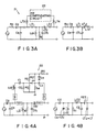
- Fig. 3A is a circuit diagram which shows an equivalent circuit of the FM compensating circuit 21 and the antenna in the FM frequency band.
- Fig. 3B shows an equivalent circuit particularly showing the parts related to the FM frequency characteristics.
- the stray capacitance Cs is small, i.e., 10 PF or less. Accordingly, as seen from Fig. 1, the FM compensating circuit 21 (i.e., the circuit which matches the antenna 10 and the feeder line 30) can be constructed using passive elements only. As a result, there is no distortion in the case of strong input signals, and the overall cost of the antenna is lower than it is when active elements are used. Moreover, there is no need for a power source.
- a double-tuned circuit including the antenna 10 is formed, impedance matching between the antenna 10 and the feeder line 30 can be favorably accomplished. Also, a broad band width can be obtained which allows coverage of the entire FM broadcast band.
- the antenna 10 since the antenna 10 is in a non-resonant state, it has a reactance component. Accordingly, circuit loss can be minimized and circuit simplification can be achieved by selecting the circuit constants of the primary side resonance circuit of the double-tuned circuit so that the resonance circuit resources in the FM frequency band (including the antenna reactance and stray capacitance Cs).
- a circuit which matches the antenna 10 and feeder line 30 can be constructed using only passive elements.
- the band width required for FM broadcast reception can be obtained by appropriately selecting the coupling capacitance Cfc, and the antenna 10 and feeder line 30 can be effectively matched by appropriately selecting the capacitance ratio of the capacitance component Ca of the antenna 10 to the capacitor Cf2.
- Fig. 5 shows the reflection loss characteristics looking at the antenna side from the output terminal of the embodiment.
- Fig. 4A is a circuit diagram which shows an equivalent circuit of the AM compensating circuit 22 and the antennas in the AM frequency band.
- Fig. 4B shows an equivalent circuit particularly showing the parts related to the AM frequency characteristics.
- the FET in the AM compensating circuit 22 performs an active impedance conversion, so that the output impedance of the AM compensating circuit 22 is lowered to a value of approximately 100 to 200 ohms. Accordingly, the capacitance splitting loss arising from the feeder line 30 can be reduced to such an extent that it can virtually be ignored. In other words, even if a capacitance of 150 to 300 PF is connected in parallel with the output of the FET, such a capacitance will have almost no effect, because the output impedance of the AM compensating circuit 22 is low. Accordingly, a 50 to 75 ohm coaxial cable, which is optimal for FM transmission, can be used as the feeder line 30.
- the FET Since the FET is caused to act as a source follower, the input-output characteristics can be caused to act in a linear manner up to approximately 1/2 the DC power supply voltage. As a result, operation which is free from various types of non-linear distortion can be achieved up to a strong input signal of approximately 130 dB u. Accordingly, absolutely no problem would arise under normal use.
- the present invention which is for an automobile radio antenna used in a state shorter than the resonant state of the antenna, distortion of the received sound in cases where strong electromagnetic waves are received can be prevented, and faulty reception can be prevented in cases where it is desired to receive other waves among strong electromagnetic waves.
- the compensating circuits are inexpensive.
Landscapes
- Input Circuits Of Receivers And Coupling Of Receivers And Audio Equipment (AREA)
- Details Of Aerials (AREA)
- Noise Elimination (AREA)
Applications Claiming Priority (2)
| Application Number | Priority Date | Filing Date | Title |
|---|---|---|---|
| JP1058790A JPH02237303A (ja) | 1989-03-10 | 1989-03-10 | 補償回路付き短縮マストアンテナ |
| JP58790/89 | 1989-03-10 |
Publications (2)
| Publication Number | Publication Date |
|---|---|
| EP0387003A1 true EP0387003A1 (fr) | 1990-09-12 |
| EP0387003B1 EP0387003B1 (fr) | 1995-03-15 |
Family
ID=13094369
Family Applications (1)
| Application Number | Title | Priority Date | Filing Date |
|---|---|---|---|
| EP90302377A Expired - Lifetime EP0387003B1 (fr) | 1989-03-10 | 1990-03-06 | Antenne tige écourtée à circuits de compensation |
Country Status (5)
| Country | Link |
|---|---|
| US (1) | US5398036A (fr) |
| EP (1) | EP0387003B1 (fr) |
| JP (1) | JPH02237303A (fr) |
| DE (1) | DE69017731T2 (fr) |
| ES (1) | ES2072388T3 (fr) |
Cited By (1)
| Publication number | Priority date | Publication date | Assignee | Title |
|---|---|---|---|---|
| WO2001003235A1 (fr) * | 1999-06-30 | 2001-01-11 | Calearo Srl | Antenne multiusages pour vehicules |
Families Citing this family (4)
| Publication number | Priority date | Publication date | Assignee | Title |
|---|---|---|---|---|
| JP3015275B2 (ja) * | 1995-04-10 | 2000-03-06 | 株式会社ワコム | 位置検出装置およびそれに用いる位置指示器 |
| GB9508592D0 (en) * | 1995-04-27 | 1995-06-14 | Rca Thomson Licensing Corp | Rf filter and agc circuit |
| WO2001095507A2 (fr) * | 2000-06-09 | 2001-12-13 | Daimlerchrysler Ag | Agencement pour faire fonctionner plusieurs terminaux |
| DE102012025319B4 (de) * | 2012-12-22 | 2019-10-10 | Diehl Defence Gmbh & Co. Kg | Verfahren zum Verarbeiten eines Navigationssatelliten-Signals und Empfänger für ein Navigationssatelliten-Signal |
Citations (3)
| Publication number | Priority date | Publication date | Assignee | Title |
|---|---|---|---|---|
| US3939423A (en) * | 1974-07-01 | 1976-02-17 | Viktor Ivanovich Zakharov | Automobile active receiving antenna |
| FR2452803A1 (fr) * | 1978-03-10 | 1980-10-24 | Blankenburg Antennen | Antenne a amplificateur electronique et destinee a la reception de plusieurs gammes d'ondes |
| EP0023943A1 (fr) * | 1979-08-11 | 1981-02-18 | Robert Bosch Gmbh | Circuit de réception et d'amplification de signaux à hautes fréquences |
Family Cites Families (9)
| Publication number | Priority date | Publication date | Assignee | Title |
|---|---|---|---|---|
| US2021734A (en) * | 1932-05-14 | 1935-11-19 | Int Communications Lab Inc | Transmission line network for radio receiving antennae |
| US2810070A (en) * | 1954-06-18 | 1957-10-15 | Acf Ind Inc | Automatic antenna tuner |
| DE2115657C3 (de) * | 1971-03-31 | 1983-12-22 | Flachenecker, Gerhard, Prof. Dr.-Ing., 8012 Ottobrunn | Aktive Unipol-Empfangsantenne |
| US3965426A (en) * | 1974-01-10 | 1976-06-22 | Tandy Corporation | Frequency modulated signal pre-amplifier with amplitude modulated signal bypass |
| US4228544A (en) * | 1978-01-19 | 1980-10-14 | Guyton James H | Antenna system using antenna base impedance transforming means |
| JPS5713823A (en) * | 1980-06-30 | 1982-01-23 | Harada Kogyo Kk | Antenna device |
| JPH0654879B2 (ja) * | 1985-10-14 | 1994-07-20 | 原田工業株式会社 | 自動車の短縮アンテナ用同調回路 |
| US4850034A (en) * | 1987-08-27 | 1989-07-18 | Campbell Mark E | Method and apparatus for installing a cellular telephone in a vehicle |
| US5151708A (en) * | 1989-03-10 | 1992-09-29 | Harada Kogyo Kabushiki Kaisha | Shortened mast antenna with compensating circuits |
-
1989
- 1989-03-10 JP JP1058790A patent/JPH02237303A/ja active Pending
-
1990
- 1990-03-06 DE DE69017731T patent/DE69017731T2/de not_active Expired - Fee Related
- 1990-03-06 EP EP90302377A patent/EP0387003B1/fr not_active Expired - Lifetime
- 1990-03-06 ES ES90302377T patent/ES2072388T3/es not_active Expired - Lifetime
-
1992
- 1992-12-28 US US07/999,190 patent/US5398036A/en not_active Expired - Fee Related
Patent Citations (3)
| Publication number | Priority date | Publication date | Assignee | Title |
|---|---|---|---|---|
| US3939423A (en) * | 1974-07-01 | 1976-02-17 | Viktor Ivanovich Zakharov | Automobile active receiving antenna |
| FR2452803A1 (fr) * | 1978-03-10 | 1980-10-24 | Blankenburg Antennen | Antenne a amplificateur electronique et destinee a la reception de plusieurs gammes d'ondes |
| EP0023943A1 (fr) * | 1979-08-11 | 1981-02-18 | Robert Bosch Gmbh | Circuit de réception et d'amplification de signaux à hautes fréquences |
Cited By (1)
| Publication number | Priority date | Publication date | Assignee | Title |
|---|---|---|---|---|
| WO2001003235A1 (fr) * | 1999-06-30 | 2001-01-11 | Calearo Srl | Antenne multiusages pour vehicules |
Also Published As
| Publication number | Publication date |
|---|---|
| DE69017731D1 (de) | 1995-04-20 |
| US5398036A (en) | 1995-03-14 |
| ES2072388T3 (es) | 1995-07-16 |
| JPH02237303A (ja) | 1990-09-19 |
| DE69017731T2 (de) | 1995-11-16 |
| EP0387003B1 (fr) | 1995-03-15 |
Similar Documents
| Publication | Publication Date | Title |
|---|---|---|
| US4395713A (en) | Transit antenna | |
| US4085405A (en) | Antenna matching network | |
| US5089829A (en) | Antenna device shared by three kinds of waves | |
| US4764773A (en) | Mobile antenna and through-the-glass impedance matched feed system | |
| EP0334297B1 (fr) | Instrument sans fil porté au poignet | |
| US4228544A (en) | Antenna system using antenna base impedance transforming means | |
| US3699452A (en) | Active antenna arrangement for a plurality of frequency ranges | |
| US3965426A (en) | Frequency modulated signal pre-amplifier with amplitude modulated signal bypass | |
| US5398036A (en) | Shortened mast antenna with compensating circuits | |
| US5151708A (en) | Shortened mast antenna with compensating circuits | |
| JPH10209897A (ja) | 可変同調型アンテナ装置 | |
| US5978663A (en) | Antenna tuning circuit | |
| US5598170A (en) | Glass antenna for automobiles | |
| US5548298A (en) | Glass antenna for automobiles | |
| US6933984B2 (en) | Television tuner which maintains UHF band tuning circuit bandwidth constant in low to high band range | |
| JP2001036328A (ja) | Am・fm帯受信用アンテナ | |
| JPH0654879B2 (ja) | 自動車の短縮アンテナ用同調回路 | |
| JPH03158003A (ja) | 補償回路付き短縮マストアンテナ | |
| US4596044A (en) | UHF-VHF combination tuner | |
| US4352107A (en) | Matching cable for automobile antennas for receiving FM broadcasts | |
| JPH11308038A (ja) | アンテナおよびアンテナ装置 | |
| EP1061659B1 (fr) | Récepteur multibande | |
| US5173712A (en) | Rod antenna with filter arrangement | |
| KR880002103B1 (ko) | 차단 및 정합회로를 가진 전기신호 분리장치 | |
| JP3115540B2 (ja) | Am・fm受信用アンテナ |
Legal Events
| Date | Code | Title | Description |
|---|---|---|---|
| PUAI | Public reference made under article 153(3) epc to a published international application that has entered the european phase |
Free format text: ORIGINAL CODE: 0009012 |
|
| 17P | Request for examination filed |
Effective date: 19900320 |
|
| AK | Designated contracting states |
Kind code of ref document: A1 Designated state(s): DE ES FR GB IT SE |
|
| 17Q | First examination report despatched |
Effective date: 19930504 |
|
| GRAA | (expected) grant |
Free format text: ORIGINAL CODE: 0009210 |
|
| AK | Designated contracting states |
Kind code of ref document: B1 Designated state(s): DE ES FR GB IT SE |
|
| ITF | It: translation for a ep patent filed | ||
| REF | Corresponds to: |
Ref document number: 69017731 Country of ref document: DE Date of ref document: 19950420 |
|
| ET | Fr: translation filed | ||
| REG | Reference to a national code |
Ref country code: ES Ref legal event code: FG2A Ref document number: 2072388 Country of ref document: ES Kind code of ref document: T3 |
|
| PLBE | No opposition filed within time limit |
Free format text: ORIGINAL CODE: 0009261 |
|
| STAA | Information on the status of an ep patent application or granted ep patent |
Free format text: STATUS: NO OPPOSITION FILED WITHIN TIME LIMIT |
|
| 26N | No opposition filed | ||
| REG | Reference to a national code |
Ref country code: GB Ref legal event code: IF02 |
|
| PGFP | Annual fee paid to national office [announced via postgrant information from national office to epo] |
Ref country code: FR Payment date: 20030210 Year of fee payment: 14 |
|
| PGFP | Annual fee paid to national office [announced via postgrant information from national office to epo] |
Ref country code: GB Payment date: 20030305 Year of fee payment: 14 |
|
| PGFP | Annual fee paid to national office [announced via postgrant information from national office to epo] |
Ref country code: ES Payment date: 20030317 Year of fee payment: 14 |
|
| PGFP | Annual fee paid to national office [announced via postgrant information from national office to epo] |
Ref country code: SE Payment date: 20030318 Year of fee payment: 14 |
|
| PGFP | Annual fee paid to national office [announced via postgrant information from national office to epo] |
Ref country code: DE Payment date: 20030429 Year of fee payment: 14 |
|
| PG25 | Lapsed in a contracting state [announced via postgrant information from national office to epo] |
Ref country code: GB Free format text: LAPSE BECAUSE OF NON-PAYMENT OF DUE FEES Effective date: 20040306 |
|
| PG25 | Lapsed in a contracting state [announced via postgrant information from national office to epo] |
Ref country code: SE Free format text: LAPSE BECAUSE OF NON-PAYMENT OF DUE FEES Effective date: 20040307 |
|
| PG25 | Lapsed in a contracting state [announced via postgrant information from national office to epo] |
Ref country code: ES Free format text: LAPSE BECAUSE OF NON-PAYMENT OF DUE FEES Effective date: 20040308 |
|
| PG25 | Lapsed in a contracting state [announced via postgrant information from national office to epo] |
Ref country code: DE Free format text: LAPSE BECAUSE OF NON-PAYMENT OF DUE FEES Effective date: 20041001 |
|
| GBPC | Gb: european patent ceased through non-payment of renewal fee | ||
| EUG | Se: european patent has lapsed | ||
| PG25 | Lapsed in a contracting state [announced via postgrant information from national office to epo] |
Ref country code: FR Free format text: LAPSE BECAUSE OF NON-PAYMENT OF DUE FEES Effective date: 20041130 |
|
| REG | Reference to a national code |
Ref country code: FR Ref legal event code: ST |
|
| PG25 | Lapsed in a contracting state [announced via postgrant information from national office to epo] |
Ref country code: IT Free format text: LAPSE BECAUSE OF NON-PAYMENT OF DUE FEES Effective date: 20050306 |
|
| REG | Reference to a national code |
Ref country code: ES Ref legal event code: FD2A Effective date: 20040308 |