EP0388149A2 - Halbleiterlaser und Verfahren zur Herstellung desselben - Google Patents
Halbleiterlaser und Verfahren zur Herstellung desselben Download PDFInfo
- Publication number
- EP0388149A2 EP0388149A2 EP90302666A EP90302666A EP0388149A2 EP 0388149 A2 EP0388149 A2 EP 0388149A2 EP 90302666 A EP90302666 A EP 90302666A EP 90302666 A EP90302666 A EP 90302666A EP 0388149 A2 EP0388149 A2 EP 0388149A2
- Authority
- EP
- European Patent Office
- Prior art keywords
- band
- graded
- semiconductor laser
- gap layer
- laser device
- Prior art date
- Legal status (The legal status is an assumption and is not a legal conclusion. Google has not performed a legal analysis and makes no representation as to the accuracy of the status listed.)
- Granted
Links
Images



Classifications
-
- H—ELECTRICITY
- H01—ELECTRIC ELEMENTS
- H01S—DEVICES USING THE PROCESS OF LIGHT AMPLIFICATION BY STIMULATED EMISSION OF RADIATION [LASER] TO AMPLIFY OR GENERATE LIGHT; DEVICES USING STIMULATED EMISSION OF ELECTROMAGNETIC RADIATION IN WAVE RANGES OTHER THAN OPTICAL
- H01S5/00—Semiconductor lasers
- H01S5/02—Structural details or components not essential to laser action
- H01S5/028—Coatings ; Treatment of the laser facets, e.g. etching, passivation layers or reflecting layers
- H01S5/0281—Coatings made of semiconductor materials
-
- H—ELECTRICITY
- H01—ELECTRIC ELEMENTS
- H01S—DEVICES USING THE PROCESS OF LIGHT AMPLIFICATION BY STIMULATED EMISSION OF RADIATION [LASER] TO AMPLIFY OR GENERATE LIGHT; DEVICES USING STIMULATED EMISSION OF ELECTROMAGNETIC RADIATION IN WAVE RANGES OTHER THAN OPTICAL
- H01S5/00—Semiconductor lasers
- H01S5/02—Structural details or components not essential to laser action
- H01S5/0201—Separation of the wafer into individual elements, e.g. by dicing, cleaving, etching or directly during growth
-
- H—ELECTRICITY
- H01—ELECTRIC ELEMENTS
- H01S—DEVICES USING THE PROCESS OF LIGHT AMPLIFICATION BY STIMULATED EMISSION OF RADIATION [LASER] TO AMPLIFY OR GENERATE LIGHT; DEVICES USING STIMULATED EMISSION OF ELECTROMAGNETIC RADIATION IN WAVE RANGES OTHER THAN OPTICAL
- H01S5/00—Semiconductor lasers
- H01S5/10—Construction or shape of the optical resonator, e.g. extended or external cavity, coupled cavities, bent-guide, varying width, thickness or composition of the active region
- H01S5/16—Window-type lasers, i.e. with a region of non-absorbing material between the active region and the reflecting surface
- H01S5/164—Window-type lasers, i.e. with a region of non-absorbing material between the active region and the reflecting surface with window regions comprising semiconductor material with a wider bandgap than the active layer
-
- H—ELECTRICITY
- H01—ELECTRIC ELEMENTS
- H01S—DEVICES USING THE PROCESS OF LIGHT AMPLIFICATION BY STIMULATED EMISSION OF RADIATION [LASER] TO AMPLIFY OR GENERATE LIGHT; DEVICES USING STIMULATED EMISSION OF ELECTROMAGNETIC RADIATION IN WAVE RANGES OTHER THAN OPTICAL
- H01S5/00—Semiconductor lasers
- H01S5/10—Construction or shape of the optical resonator, e.g. extended or external cavity, coupled cavities, bent-guide, varying width, thickness or composition of the active region
- H01S5/16—Window-type lasers, i.e. with a region of non-absorbing material between the active region and the reflecting surface
- H01S5/166—Window-type lasers, i.e. with a region of non-absorbing material between the active region and the reflecting surface with window regions comprising non-semiconducting materials
Definitions
- This invention relates to a semiconductor laser device which emits laser light from an end facet thereof and it also relates to a method for the production of such a semiconductor laser device.
- semiconductor laser devices have widely come into practical use as light sources for optical disc driving units.
- semiconductor laser devices are used as the light source for write-once optical disc driving units or rewritable optical disc driving units, they are required to have high reliability even at a high output power level of from 40 to 50 mW.
- an output power of 100 mW or more is required.
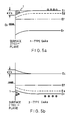
- FIGS 5a and 5b are schematic diagrams showing the energy band structures near the surface originating from the surface state which occurs when either the n-type or p-type GaAs (110)-surface is slightly oxidized.
- n-type or p-type GaAs numerous carriers accumulate near the surface to form a so-called “accumulation layer” which is indicated by reference numeral 1 in these figures.
- an accumulation layer 1 which is a local inversion of the conductivity type.
- an accumulation layer 1 or an inversion layer 2 forms, is dependent on the height relationship between the surface state E s and the Fermi level E f of the semiconductor. In either case of n-type or p-type GaAs, an accumulation layer 1 will form.
- the heat released from the surface state concentrates at the end facets of the semiconductor, and this heat narrows the forbidden band gap in the energy bands. Furthermore, the absorption of light increases the minority carriers, and heat generation further increases by way of the surface state. This process raises the temperature of the semiconductor surface, which may reach the melting point of the semiconductor, resulting in facet breakdown.
- an accumulation layer forms, while in the case of other materials such as AlGaAs, an inversion layer may form. In the latter case, majority carriers are trapped in the surface state, and facet breakdown occurs by the same process as that by an accumulation layer. In the case of semiconductor laser devices used under a high injection condition, heat generation originating with the surface state becomes a more serious problem.
- a method for preventing the effect of surface recombination there has been proposed a method in which a region having a graded band gap is formed near the surface.
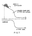
- a solar cell having a graded-band-gap layer formed by liquid phase epitaxy is disclosed by M. Konagai and K. Takahashi, J. Appl. Phys. Vol. 46 No. 8, pp. 3542-3546 August (1975).
- Figure 7 shows a schematic energy band diagram of a graded-band-gap heterojunction solar cell described in the above-identified prior art reference.
- a graded-band-gap layer can be formed by liquid phase epitaxy during the crystal growth, thereby attaining the effective suppression of surface recombination.
- a light-emitting facet which may be adversely affected by surface recombination, is usually formed by a cleavage of semiconductor crystals. Therefore, it is extremely difficult to form a graded-band-gap layer in advance on the cleavage plane by liquid phase epitaxy. For this reason, conventional semiconductor laser devices have a serious problem of causing facet breakdown due to surface recombination at the light-emitting facet.
- the semiconductor laser device of this invention which overcomes the above-discussed and numerous other disadvantages and deficiencies of the prior art, comprises a multi-layered structure formed on a semiconductor substrate, the multi-layered structure having an active layer for laser oscillation, and a pair of cleavage planes on the side of the multi-layered structure, the device wherein a graded-band-gap layer is formed on at least one of the cleavage planes, the graded-band-gap layer having a forbidden band gap which increases gradually with an increase in the distance from the cleavage plane, and the surface of the graded-band-gap layer constituting an end facet of the device.
- the active layer is made of Ga 1-x Al x As (0 ⁇ x ⁇ 1) and the graded-band-gap layer is made of Ga 1-y Al y As.
- the Al mole fraction y of the graded-band-gap layer increases from the cleavage plane to the end facet in accordance with the linear or parabolic distribution.
- the above-mentioned Al mole fraction y at the cleavage plane between the active layer and the graded-band-gap layer is equal to the Al mole fraction x.
- the above-mentioned Al mole fraction y at the cleavage plane between the active layer and the graded-band-gap layer is greater than the Al mole fraction x.
- the above-mentioned Al mole fraction y at the cleavage plane between the active layer and the graded-band-gap layer is smaller than the Al mole fraction x.
- the method of this invention for the production of a semiconductor laser device comprises forming a multi-layered structure on a semiconductor substrate, the multi-layered structure having an active layer for laser oscillation; cleaving the substrate together with the multi-layered structure to form a laser cavity between cleavage planes; and forming a graded-band-gap layer on at least one of the cleavage planes, the graded-band-gap layer having a forbidden band gap which increases gradually with an increase in the distance from the cleavage plane.
- the graded-band-gap layer is grown by vapor phase epitaxy.
- the invention described herein makes possible the objectives of (1) providing a semi-conductor laser device with a construction capable of suppressing the surface state in the vicinity of the light-emitting facet so that facet breakdown does not occur easily even in high output power conditions; (2) providing a semiconductor laser device in which a graded-band-gap layer is formed on the cleavage plane, and therefore, electrons generated near the end facet are rapidly separated from the end facet, so that facet breakdown due to surface recombination can be effectively suppressed, thereby attaining the improved output power with high reliability; and (3) providing a method for the production of such a semiconductor laser device with excellent characteristics.
- the semiconductor laser device of this invention has the same structure as that of a conventional semiconductor laser device which emits laser light from an end facet thereof, except that a graded-band-gap layer is formed on at least one of the cleavage planes.
- the graded-band-gap layer has a forbidden band gap which increases gradually with an increase in the distance from the cleavage plane.
- the surface of the graded-band-gap layer constitutes the end facet of the device.
- Figure 1 is a perspective view showing the front facet area of a semiconductor laser device of this invention. The production process of this semiconductor laser device is explained below.
- a multi-layered structure 12 including an active layer 16 for laser oscillation is grown on a semiconductor substrate 11 .
- the active layer 16 is made of, for example, Ga 1-x Al x As (0 ⁇ x ⁇ 1).
- the method for the growth of the multi-layered structure 12 including the active layer 16 can be any one of the conventional processes such as liquid phase epitaxy and vapor phase epitaxy.
- the wafer thus obtained is cleaved by a known cleavage method so as to obtain the prescribed cavity length, resulting in a plurality of bars 15 as shown in Figure 2b.
- Each of the bars 15 has a plurality of cavity units arranged in the direction perpendicular to the cavity direction.
- SiO2 film 20 is formed by plasma chemical vapor deposition or other similar processes as shown in Figure 2c.
- a graded-band-gap layer 18 is formed by molecular beam epitaxy or metal organic chemical vapor deposition.
- the active layer 16 is made of Ga 1-x Al x As (0 ⁇ x ⁇ 1)
- the graded-band-gap layer 18 is also made of Ga 1-y Al y As in which the Al mole fraction y increases gradually from the Al mole fraction x of the active layer 16 to the prescribed final value at the end facet.
- the GaAlAs layer grown on the SiO2 film 20 is made of polycrystallines, and such a polycrystalline GaAlAs layer can readily be removed by an etching technique after growth. Accordingly, the graded-band-gap layer 18 can be formed only on the cleavage plane which corresponds to the light-emitting facet of the laser cavity.
- ohmic electrodes 13 and 14 were formed on the upper face of the multi-layered structure 12 and the back face of the semiconductor substrate 11 , respectively.
- the method for the formation of the ohmic electrodes 13 and 14 can be any one of the conventional processes.
- an SiO2 film may be formed on the upper face of the multi-layered structure 12 and the back face of the semiconductor substrate 11 , followed by cleavage of the wafer thus obtained.
- the cleavage of the wafer can immediately provide a bar 15 as shown in Figure 2c.
- a semiconductor laser device was produced with the above-mentioned constitution, in which the Al mole fraction x of the active layer 16 was set to 0.14 and the Al mole fraction y of the graded-band-gap layer 18 was varied as shown in Figure 3a.
- the thickness of the graded-band-gap layer 18 was 0.1 ⁇ m.
- the semiconductor laser device thus obtained was then provided with coatings on both end facets such that the reflectivity of the light-emitting facet became 4% and the reflectivity of the other facet 95%.
- a conventional semiconductor laser device was produced in the same way as mentioned above, except that no graded-band-gap layer was formed on the cleavage planes.
- Figure 4 is a graph showing the injected current-optical output characteristics of the semiconductor laser device of this example obtained above (curve A) and the conventional semiconductor laser device obtained above (curve B).
- curve A the semiconductor laser device of this example obtained above
- curve B the conventional semiconductor laser device obtained above
- deterioration of the device characteristics occurs due to facet breakdown at an optical output power of approximately 200 mW
- the semiconductor laser device of this example can attain stable laser oscillation even at an optical output power of up to about 600 mW without causing facet breakdown.
- the Al mole fraction y of the graded-band-gap layer was varied in accordance with the linear distribution as shown in Figure 3a, it may also be varied in accordance with the parabolic distribution. Moreover, the Al mole fraction y is not limited to the final value of 0.5 as shown in Figure 3a, but it can takes any final value so long as it increases gradually with an increase in the distance from the cleavage plane.
- the Al mole fraction y of the graded-band-gap layer at the cleavage plane may be greater than the Al mole fraction x of the active layer.
- a barrier against electrons at the cleavage plane that is, the Al mole fraction y of the graded-band-gap layer at the cleavage plane may be smaller than the Al mole fraction x of the active layer.
- semiconductor laser devices In general, besides the carriers generated by the absorption of light, semiconductor laser devices contain additional carriers injected in the active layer from the outside. Therefore, the active layer has a high density of carriers.
- the semiconductor laser device of this invention carriers present in the vicinity of the light-emitting facet can be rapidly separated from the end facet due to the drift as well as the diffusion, resulting in an extremely small probability that these electrons contribute to heat generation via the surface state. Therefore, deterioration of the end facets can be effectively suppressed and the semiconductor laser device of this invention can attain stable laser oscillation at high output power for a long period of time.
Landscapes
- Physics & Mathematics (AREA)
- Condensed Matter Physics & Semiconductors (AREA)
- General Physics & Mathematics (AREA)
- Electromagnetism (AREA)
- Optics & Photonics (AREA)
- Semiconductor Lasers (AREA)
Applications Claiming Priority (2)
| Application Number | Priority Date | Filing Date | Title |
|---|---|---|---|
| JP1060422A JPH07109924B2 (ja) | 1989-03-13 | 1989-03-13 | 半導体レーザ装置及びその製造方法 |
| JP60422/89 | 1989-03-13 |
Publications (3)
| Publication Number | Publication Date |
|---|---|
| EP0388149A2 true EP0388149A2 (de) | 1990-09-19 |
| EP0388149A3 EP0388149A3 (de) | 1991-08-07 |
| EP0388149B1 EP0388149B1 (de) | 1995-01-25 |
Family
ID=13141760
Family Applications (1)
| Application Number | Title | Priority Date | Filing Date |
|---|---|---|---|
| EP90302666A Expired - Lifetime EP0388149B1 (de) | 1989-03-13 | 1990-03-13 | Halbleiterlaser und Verfahren zur Herstellung desselben |
Country Status (4)
| Country | Link |
|---|---|
| US (1) | US5022037A (de) |
| EP (1) | EP0388149B1 (de) |
| JP (1) | JPH07109924B2 (de) |
| DE (1) | DE69016230T2 (de) |
Cited By (2)
| Publication number | Priority date | Publication date | Assignee | Title |
|---|---|---|---|---|
| EP0477033A3 (en) * | 1990-09-21 | 1992-07-01 | Sharp Kabushiki Kaisha | A semiconductor laser device and a method for producing the same |
| US6590920B1 (en) | 1998-10-08 | 2003-07-08 | Adc Telecommunications, Inc. | Semiconductor lasers having single crystal mirror layers grown directly on facet |
Families Citing this family (3)
| Publication number | Priority date | Publication date | Assignee | Title |
|---|---|---|---|---|
| JPH0834337B2 (ja) * | 1990-04-02 | 1996-03-29 | シャープ株式会社 | 半導体レーザ素子の製造方法 |
| JP2981315B2 (ja) * | 1990-10-19 | 1999-11-22 | シャープ株式会社 | 半導体レーザ素子 |
| US5491711A (en) * | 1993-11-04 | 1996-02-13 | The Furukawa Electric Co., Ltd. | Semiconductor laser device |
Family Cites Families (5)
| Publication number | Priority date | Publication date | Assignee | Title |
|---|---|---|---|---|
| JPS559480A (en) * | 1978-07-07 | 1980-01-23 | Nec Corp | Large light output, lateral mode of semiconductor laser element |
| JPS5527474A (en) * | 1978-08-19 | 1980-02-27 | Arata Kogyosho:Kk | Manufacture of spherical head for use of oiler or the like of diesel engine |
| JPS57170585A (en) * | 1981-04-14 | 1982-10-20 | Nec Corp | Semiconductor laser device |
| JPS60113983A (ja) * | 1983-11-26 | 1985-06-20 | Mitsubishi Electric Corp | 半導体発光装置およびその製造方法 |
| JPH01138784A (ja) * | 1987-11-25 | 1989-05-31 | Nec Corp | 半導体レーザの端面保護膜形成方法 |
-
1989
- 1989-03-13 JP JP1060422A patent/JPH07109924B2/ja not_active Expired - Fee Related
-
1990
- 1990-03-08 US US07/489,180 patent/US5022037A/en not_active Expired - Lifetime
- 1990-03-13 EP EP90302666A patent/EP0388149B1/de not_active Expired - Lifetime
- 1990-03-13 DE DE69016230T patent/DE69016230T2/de not_active Expired - Fee Related
Cited By (4)
| Publication number | Priority date | Publication date | Assignee | Title |
|---|---|---|---|---|
| EP0477033A3 (en) * | 1990-09-21 | 1992-07-01 | Sharp Kabushiki Kaisha | A semiconductor laser device and a method for producing the same |
| US5228047A (en) * | 1990-09-21 | 1993-07-13 | Sharp Kabushiki Kaisha | Semiconductor laser device and a method for producing the same |
| EP0697756A3 (de) * | 1990-09-21 | 1996-07-17 | Sharp Kk | Halbleiterlaservorrichtung und Herstellungsverfahren |
| US6590920B1 (en) | 1998-10-08 | 2003-07-08 | Adc Telecommunications, Inc. | Semiconductor lasers having single crystal mirror layers grown directly on facet |
Also Published As
| Publication number | Publication date |
|---|---|
| JPH07109924B2 (ja) | 1995-11-22 |
| EP0388149A3 (de) | 1991-08-07 |
| DE69016230T2 (de) | 1995-07-27 |
| DE69016230D1 (de) | 1995-03-09 |
| EP0388149B1 (de) | 1995-01-25 |
| US5022037A (en) | 1991-06-04 |
| JPH02239680A (ja) | 1990-09-21 |
Similar Documents
| Publication | Publication Date | Title |
|---|---|---|
| US5212701A (en) | Semiconductor surface emitting laser having enhanced optical confinement | |
| US5028563A (en) | Method for making low tuning rate single mode PbTe/PbEuSeTe buried heterostructure tunable diode lasers and arrays | |
| US5455429A (en) | Semiconductor devices incorporating p-type and n-type impurity induced layer disordered material | |
| US4845725A (en) | Window laser with high power reduced divergence output | |
| EP0261262B1 (de) | Streifenlaser mit transversalem Übergang | |
| GB2222307A (en) | Semiconductor laser | |
| GB2145281A (en) | Surface emitting semiconductor laser | |
| US5608753A (en) | Semiconductor devices incorporating p-type and n-type impurity induced layer disordered material | |
| US4716125A (en) | Method of producing semiconductor laser | |
| US6654397B2 (en) | Semiconductor laser device and manufacturing method thereof | |
| US5022037A (en) | Semiconductor laser device | |
| US5574745A (en) | Semiconductor devices incorporating P-type and N-type impurity induced layer disordered material | |
| EP0544968B1 (de) | Auf einer strukturierten Substratoberfläche aufgewachsene Halbleiter-Laserdiode | |
| US5018158A (en) | Semiconductor laser device | |
| CA2106596C (en) | Semiconductor laser device | |
| EP0915542B1 (de) | Halbleiterlaser mit verbesserten stromsperrenden Schichten und Herstellungsverfahren | |
| US4943971A (en) | Low tuning rate single mode PbTe/PbEuSeTe buried heterostructure tunable diode lasers and arrays | |
| US4841535A (en) | Semiconductor laser device | |
| US4375686A (en) | Semiconductor laser | |
| JP3763459B2 (ja) | 半導体レーザ素子及びその製造方法 | |
| US5119388A (en) | Low tuning rate PbTe/PbEuSeTe buried quantum well tunable diode lasers and arrays | |
| JP2624881B2 (ja) | 半導体レーザ素子およびその製造方法 | |
| JP2927661B2 (ja) | スーパールミネッセントダイオード素子およびその製造方法 | |
| EP0867949B1 (de) | Lichtemittierende Halbleitervorrichtung | |
| JP2679974B2 (ja) | 半導体レーザ装置 |
Legal Events
| Date | Code | Title | Description |
|---|---|---|---|
| PUAI | Public reference made under article 153(3) epc to a published international application that has entered the european phase |
Free format text: ORIGINAL CODE: 0009012 |
|
| 17P | Request for examination filed |
Effective date: 19900326 |
|
| AK | Designated contracting states |
Kind code of ref document: A2 Designated state(s): DE FR GB |
|
| PUAL | Search report despatched |
Free format text: ORIGINAL CODE: 0009013 |
|
| AK | Designated contracting states |
Kind code of ref document: A3 Designated state(s): DE FR GB |
|
| 17Q | First examination report despatched |
Effective date: 19921005 |
|
| GRAA | (expected) grant |
Free format text: ORIGINAL CODE: 0009210 |
|
| AK | Designated contracting states |
Kind code of ref document: B1 Designated state(s): DE FR GB |
|
| REF | Corresponds to: |
Ref document number: 69016230 Country of ref document: DE Date of ref document: 19950309 |
|
| ET | Fr: translation filed | ||
| PLBE | No opposition filed within time limit |
Free format text: ORIGINAL CODE: 0009261 |
|
| STAA | Information on the status of an ep patent application or granted ep patent |
Free format text: STATUS: NO OPPOSITION FILED WITHIN TIME LIMIT |
|
| 26N | No opposition filed | ||
| REG | Reference to a national code |
Ref country code: GB Ref legal event code: IF02 |
|
| PGFP | Annual fee paid to national office [announced via postgrant information from national office to epo] |
Ref country code: FR Payment date: 20020312 Year of fee payment: 13 |
|
| PGFP | Annual fee paid to national office [announced via postgrant information from national office to epo] |
Ref country code: GB Payment date: 20020313 Year of fee payment: 13 |
|
| PGFP | Annual fee paid to national office [announced via postgrant information from national office to epo] |
Ref country code: DE Payment date: 20020327 Year of fee payment: 13 |
|
| PG25 | Lapsed in a contracting state [announced via postgrant information from national office to epo] |
Ref country code: GB Free format text: LAPSE BECAUSE OF NON-PAYMENT OF DUE FEES Effective date: 20030313 |
|
| PG25 | Lapsed in a contracting state [announced via postgrant information from national office to epo] |
Ref country code: DE Free format text: LAPSE BECAUSE OF NON-PAYMENT OF DUE FEES Effective date: 20031001 |
|
| GBPC | Gb: european patent ceased through non-payment of renewal fee |
Effective date: 20030313 |
|
| PG25 | Lapsed in a contracting state [announced via postgrant information from national office to epo] |
Ref country code: FR Free format text: LAPSE BECAUSE OF NON-PAYMENT OF DUE FEES Effective date: 20031127 |
|
| REG | Reference to a national code |
Ref country code: FR Ref legal event code: ST |