EP0388794A2 - Méthode et appareil pour optimiser le placement d'éléments et décider du placement optimal d'éléments - Google Patents
Méthode et appareil pour optimiser le placement d'éléments et décider du placement optimal d'éléments Download PDFInfo
- Publication number
- EP0388794A2 EP0388794A2 EP90104903A EP90104903A EP0388794A2 EP 0388794 A2 EP0388794 A2 EP 0388794A2 EP 90104903 A EP90104903 A EP 90104903A EP 90104903 A EP90104903 A EP 90104903A EP 0388794 A2 EP0388794 A2 EP 0388794A2
- Authority
- EP
- European Patent Office
- Prior art keywords
- placement
- paired
- cpus
- candidates
- elements
- Prior art date
- Legal status (The legal status is an assumption and is not a legal conclusion. Google has not performed a legal analysis and makes no representation as to the accuracy of the status listed.)
- Withdrawn
Links
Images


Classifications
-
- G—PHYSICS
- G06—COMPUTING OR CALCULATING; COUNTING
- G06F—ELECTRIC DIGITAL DATA PROCESSING
- G06F30/00—Computer-aided design [CAD]
- G06F30/30—Circuit design
- G06F30/39—Circuit design at the physical level
- G06F30/392—Floor-planning or layout, e.g. partitioning or placement
Definitions
- the present invention in general relates to element placement optimization method and apparatus for determining an optimal placement of constituent elements such as those of LSIs. More particularly, the present invention is concerned with element placement optimizing method and apparatus suited profitably for determining efficiently an optimal placement of the LSI constituent elements or the like within a reduced time as well as method and apparatus for making decision as to the optimal placement.
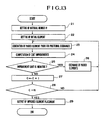
- Fig. 13 of the accompanying drawings shows a flow chart for illustrating a related art element placement optimizing method which is sometimes referred to as the repetitive improvement method.
- This known repetitive improvement method is carried out by a sequential processing type computer known heretofore. More specifically, referring to Fig. 13, the number N of times an placement improving operation is to be repeatedly executed is set at a step 21, which is then followed by setting of initial locations of individual elements by using pseudo-random numbers (step 22). Next, two paired element candidates are selected randomly by using pseudo-random numbers (step 23), whereon it is arithmetically determined to what extent the cost could be reduced on the assumption that the period element candidates were exchanged with each other in respect to the locations or positions thereof (step 24).
- a step 25 decision is made as to whether or not any cost improvement could be achieved.
- the cost for the paired element candidates will be able to be improved, e.g. when a difference resulting from subtraction of the pre-exchange cost (i.e. the cost involved unless the exchange is not performed) from the post-exchange cost has a sign of minus (negative), then the processing proceeds to a step 26 where the paired elements are exchanged in respect to the locations thereof, whereupon the step 23 is regained.
- the processing proceeds to a step 27 where the content of a counter C is incremented by "1", which is followed by a step 28 at which decision is made as to whether or not content of the counter C is greater than the number N set at the step 21.
- this decision step 28 results in that C is still smaller than N, the step 23 is regained, whereupon the processing succeeding thereto is repeated in the manner described above. If otherwise, i.e. when C is greater than N, the placement improving processing described above is terminated, and the information about the improved element placement is outputted at a step 29. Thus, the processing comes to an end.
- JP-A-62-93760 Japanese Patent Application Laid-Open No. 93670/1987
- JP-A-62-243071 JP-A-62-243071
- JP-A-62-219062 and JP-A-62-175869 discloses a processing system for deciding module placement in which each of locations or blocks for the elements is assigned with a CPU, wherein each CPU determines destinations to which the associated elements are to be moved with the aid of a procedure referred to as a gravity force directed relaxation method, the names of the element being then messaged to the CPUs belonging to the destinations. With this method, it is however difficult to realize the optimal placement for the reasons mentioned previously.
- JP-A-63-121978 has already proposed a system in which the abovementioned multi-processor method is adopted for determining stochastically whether or not the individual CPUs should perform the position exchanges in accordance with the simulated annealing method.
- a second object of the present invention is to provide an optimal placement deciding method which is capable of deciding at a high speed whether or not the placement of elements is local optimal as well as an apparatus for carrying out the same.
- a plurality of paired element candidates are selected at random, and a value of cost improvement is computed for each of the element candidate pairs, wherein only the element candidate pair having the highest value of cost improvement or alternatively the element candidate pair having a higher value of cost improvement than a given threshold value is repeatedly subjected to the processing for exchanging the element positions for a predetermined number of times or until the effect of improvement can no more be shown.
- decision as to whether or not an element placement is the optimal solution can be made at an increased speed by virtue of the feature that the placement for which a plurality of pairs of the elements selected at random are not improved in the cost is decided as to be a local optimal solution.
- the present invention can enjoy such advantageous effect that the element placement in the large size LSI and others can be optimized at a very high speed. Additionally, the use of the element placement optimizing method and apparatus is accompanied with a profitable effect that the LSI or the like having an enhanced quality can be realized. Besides, application of a parallel processing type computer to the realization of the invention enables the processing to be further promoted with overhead being reduced.
- Fig. 1 shows in a block diagram a general placement of the element placement optimizing apparatus according to an exemplary embodiment of the invention.
- a parallel processing type computer system is employed. It should however be appreciated that a sequential processing type computer can equally be used.
- the element placement optimizing apparatus includes a condition setting input part 10, an initial placement setting part 11, a connection table 12 and an element position table 13 both stored in a storage or memory, a parallel-type placement improving computation part 14, an evaluation/decision part 15 and an output part 16.
- the initial arrangement setting part 11 sets or establishes an initial placement of constituents or elements at random by using preudo-random numbers or through an empirical or heuristic procedure such as, for example, a minimum cut method mentioned hereinafter or the like in accordance with the conditions inputted through an input part 10.
- connection table 12 contains information about wiring or interconnecting relations among the elements. This table is initialized by the information supplied from the initial placement setting part 11.
- the element position table 13 stores therein the information concerning the positional relationships among the individual elements. This table is initialized by the information supplied from the initial placement setting part 11 and updated by the information supplied from the evaluation/decision processing part 15. Both of the tables mentioned above is constituted by a shared memory in the case of the illustrated embodiment.
- Fig. 3 shows a structure of the connection table 12 which is a sort of net list.
- the constituent elements incorporated in a number S in a LSI are attached with the identification numbers "1" to "S", respectively.
- the information about the connection of the element numbered 1 (No. 1) is stored as shown at 201 in the table 12, the information about the connection of the element No. 2 is stored as shown at 202, and so forth. In this manner, the information concerning the elements No. 1 to No. S is arrayed in S rows in parallel with one another.
- the number (S) of the elements is stored at a position 209 located adjacent to the information No. 1.
- the element identification number (No. 1 the element identification number (No.
- Fig. 4 shows a structure of the element position table 13 containing the information about the positions of the elements, i.e. the coordinates of the individual elements.
- Information about the position of the element No. 1 is stored at 211.
- the number (S) of the elements is stored at a position 213 adjacent to the position information of the element No. 1.
- the identification number (No. 1) of that element is placed at the start position 214 in succession to which the X- coordinate (X1) and the Y-coordinate (Y1) of the element No. 1 are placed at positions 214 and 216, respectively, in this sequential order.
- the parallel processing type element placement improving computation part 14 comprises a plurality of processors 14(1), ..., 14(M) and memories 14(1a), ..., 14(Ma) provided in correspondence to the individual processors, respectively, as shown in detail in Fig. 2.
- Each of the processors 14(1), ..., 14(M) serves to select a pair of element candidates (also referred to as the paired element candidates) independent of the others by using pseudo-random numbers or the like, determine evaluation function values for evaluating the element placement before and after local change thereof (e.g.
- the evaluation/decision processing part 15 comprises a control processor 15(a) (which may be constituted by one of the processors shown in 1 which assumes initially an idle state) and a memory 15(a).
- the control processor 15(1) serves to determine the value indicating the most effective cost improvement from those computed by the individual processors incorporated in the parallel processing type placement improving computation part and stored in the respective memories, and update the associated values of the element position table 13 to the values representing the positions of the paired candidate elements which assume the determined value.
- the control processor 15(1) outputs through the output part (16) the information concerning the inter-element connection or wiring relations as well as the inter-element positional relations at that time point.
- Operation for satisfying the predetermined final condition is performed by the control processor 15(1) through cooperation with the memory 15(a).
- the control processor 15(1) there may be stored in the memory 15(a) the number (N) of times the element placement computation is to be repeated, the number (M) of the CPUs which are used for the computation processing or which is to be used upon starting the computation processing in case a number of the usable CPUs are variable, the number of the CPUs increased as the computation proceeds, the upper limit number of the CPUs which are allowed to be employed, and others.
- a threshold value for the cost improvement is established by storing a predetermined cost improvement value in the memory 15(a).
- Fig. 5 is a flow chart for illustrating a computation procedure for carrying out the element placement optimizing method according to a first embodiment of the invention.
- initial values are set at a step 31.
- N a positive integer or natural number
- M the number of the CPUs used for the aimed processing
- "1" is set as the initial value for the counter C.
- S represents the number of elements to be placed.
- M represents the number of the CPUs, and C represents the number of combinations, on the assumption, however, that the initial element placement is determined at random and that the paired elements are also selected at random.
- the predetermined value of the repetition number N is empirically determined. Assuming, by way of example only, that the number S of the elements is 50 (in practice, the number S of the elements arranged or placed on an actual LSI is approximately in the range of 50 to 100) and that the number of the CPUs is 1225, then the value of N should preferably be on the order of 60 (times).
- the initial placement of the elements is established by using, for example, pseudo-random numbers.
- Such initial placement of the elements can be specifically determined by labelling the S elements with the respective identification numbers (Nos. 1 to S), as described previously in conjunction with the connection table (Fig. 3) and the element position table (Fig. 4), and by defining S slots numbered and arrayed for allowing the S elements to be disposed thereon by the X- and Y- coordinates, wherein the initial element placement is specified by the X-Y slot numbers.
- the initial element placement can be established by determining the identification numbers of the slots where the elements are placed, respectively, by using pseudo-random numbers and determining the placements of the elements.
- step 33 M pairs of the element candidates are selected at random by using pseudo-random numbers or other, whereon the cost improvement value is computed by subtracting the cost required for the wiring or other after positional exchange of the paired elements from that required before such exchange (step 34).
- the computation to this end is performed as follows.
- the overall inter-element wiring length E is determined in accordance with the following expression: where D(i, n(j)) represents distance between an element i and an element n(j), S represents the number of elements, and P(i) represents the number of elements connected to the element i .
- E1 represents the cost value after the exchange
- E2 represents the cost value before the exchange.
- step 35 decision is made as to whether or not there exists the cost improvement value of minus (negative) sign among those computed by the M CPUs (i.e. the value indicating cost reduction due to the positional exchange of the paired element candidates). If the answer of this decision step is affirmative (yes), the processing proceeds to a step 36 where the positions of the paired elements involving the highest cost reduction are exchanged, whereupon the step 33 is regained.
- the processing proceeds to a next step 37 where the content of the counter C is incremented by "1", which is then followed by a step 38 at which the content of the counter C is compared with the predetermined repetition number N set at teh step 31.
- the comparison processing step 38 results in that the condition C > N is not satisfied, the step 33 is regained while otherwise the element placement information determined through the processing described above is outputted, whereupon the entire processing is completed. In other words, when M element pairs which can bring about the cost improvement have been selected (N + 1) times, the whole processing is then completed.
- the instant embodiment of the invention there can be achieved an advantageous effect that the local optimal element placement can be determined at a high speed.
- the parallel-processing type computer system is used (although a high-speed sequential processing computer can be used)
- the CPU overhead problem encountered in the conventional parallel processing is unlikely to occur by virtue of the feature that the individual CPUs are capable of computing the cost improvement values owing to the inter-element positional exchanges which are independent of one another.
- Fig. 6 is a flow chart for illustrating the element placement optimizing method according to a second embodiment of the present invention.
- the instant embodiment is basically similar to the first embodiment, and the steps 131, 132, 133, 134, 135, 136 and 139 shown in Fig. 6 correspond, respectively, to the steps 31, 32, 33, 34, 35, 36 and 39 of the first embodiment except the difference mentioned below.
- the computation for determining the cost improvement value for the element pairs is repeated for the predetermined number of times (N) through the processing steps 37 and 38.
- the result of the optimal placement computation can be outputted by way of the improvement placement output step 139 from the decision step 135, when there can no more be obtained the cost improvement value of minus sign.
- Fig. 7 is a flow chart for illustrating the element placement optimizing method according to a third embodiment of the present invention. This embodiment is basically similar to the first embodiment except that the use of a parallel processing type computer system is a prerequisite in order to allow other tasks to be executed in parallel with the optimal element placement determination processing.
- initial values are set. More specifically, a natural number N for deciding completion of the processing and an upper limit value M max of the number of the CPUs as employed are set with the initial values for two counters C1 and C2 being set to "1", respectively.
- an initial element placement is set, as described hereinbefore in conjunction with the step 32 of the first embodiment.
- a number of the element candidate pairs equal to the number contained in the counter C2 are selected at random, whereon the cost improvement values are computed for the selected element candidate pairs (step 44). Then, decision is made as to whether any one of the computed improvement values has minus sign (step 45). If the answer of the decision step 45 is affirmative (yes), the positions of the paired candidate elements susceptible to the highest cost improving effect (i.e. maximum cost reduction) are exchanged to each other, and then the step 43 is regained. On the other hand, when the answer of the decision step 45 is negative (no), i.e. when no cost improvement value of minus sign is found, the processing proceeds to a step 47a where the content of the counter C1 is incremented by "1".
- step 47b the content of the counter C1 is compared with the present value N at a step 41. Unless the condition that C1 > N is yet satisfied, the step 43 is ragained, while otherwise the processing proceeds to a next step 48a.
- the content of the counter C2 is incremented by "1", which is then followed by a step 48b where the content of the counter C2 is compared with the upper limit value M max .
- the condition that C2 > M max is satisfied yet, the condition that C1 > N is confirmed at a step 48c, whereon the step 43 is regained.
- the answer of the decision step 48b is affirmative (yes)
- the information of the element placement determined through the processing described above is outputted at a step 49. The processing then comes to an end.
- a first pair of elements is selected for determining the cost improvement value attainable with the positional exchange.
- the element replacement is performed. This processing is repeatedly executed.
- a second pair of the elements is selected to undergo the similar processing.
- a third pair of the elements is selected to be subjected to the similar processing.
- the number of the pairs to be selected is increased one by one (with the number of the CPUs for use in the parallel computation of the cost improvement value being correspondingly increased), and when the number of the CPUs exceeds the value M max preset at the step 41, the entire processing is completed.
- the number of the CPUs operated actually is smaller than the upper limit number M max of the usable CPUs, the extra CPUs are used for executing other task(s).
- the instant (third) embodiment of the invention can enjoy in addition to the advantageous effects similar to those of the first embodiment a further profitable effect that the processing for the optimal element placement determination may be executed in parallel with other task(s). It should be mentioned that instead of increasing the number of the CPUs one by one, it is also possible to increase it on a plural-number basis (i.e. by a predetermined number of CPUs simultaneously). Besides, it is also conceivable that priority or preference is placed on the other task(s), wherein the CPUs in excess are used for computation of the cost improvement value.
- the processing for determining the optimal element placement may be completed when the element pair susceptible to the cost improvement can no more be selected even after the computation for the cost improvement has been performed for a predetermined number of times or even after it has been carried out a predetermined number of times by using a predetermined number of CPUs.
- Fig. 8 is a flow chart for illustrating the computation procedure involved in the element placement optimizing procedure according to a fourth exemplary embodiment of the present invention.
- This embodiment differ from the first embodiment only in that the setting of the initial element placement performed at the step 32 is carried out at random but in accordance with an approximating algorithm.
- the setting in accordance with the approximating algorithm it is intended to mean the setting through empirical or heuristic procedure which is capable of setting the element placement so as to reduce the cost to an extend although not at optimum.
- the minimum cut procedure or algorithm is adopted as the heuristic procedure for the initial element placement. Since the element placement setting by the minimum cut method is fully described in the literature mentioned hereinbefore (i.e. the article by M.A. Berure), a brief description thereof will be sufficient for understanding the fourth embodiment of the inventive method.
- a cut line is defined on a LSI chip on which elements are placed at random, whereon the number of inter-element wiring conductors which traverse the cut line is determined. Subsequently, the element exchange is performed and the number of the inter-element wiring conductors traversing the cut line is determined. By determining the element placement so that the wiring conductor number is decreased, the initial placement is established.
- the instant embodiment is advantageous in that convergence to the placement equivalent to or approximating to the optimum solution can be realized within a much reduced time because of the initial placement improved at least to some extent.
- Fig. 9 is a flow chart showing a computation procedure for the element placement optimizing method according to a fifth embodiment of the invention.
- the embodiment differs from the first one in that a threshold value setting step 75 is provided and that any one of element pairs which are susceptible to the cost improvement over the threshold rather than that susceptible to the highest cost improvement or reduction is selected for the positional exchange at a step 77.
- the threshold value setting step 75 the number M1 of those of the cost improvement values determined at the step 74 which are of minus sign is determined, whereon the threshold value ⁇ is arithmetically determined by the control CPU, for example, in accordance with the following expression: where M represents the number of the pairs selected at step 73 (or the number of the CPUs used for this processing in the parallel computer system).
- Fig. 10 is a flow chart for illustrating a decision procedure in an optimal placement deciding method according to a further embodiment of the invention.
- the predetermined repetition number N and the number M of the CPUs are set at a step 61, which is followed by a step 62 where an element placement for which an extremal value decision (local optimum value decision) is to be performed is set.
- Steps 63, 64 and 65 are similar to the step 33, 34 and 35, respectively, which have been described hereinbefore in conjunction with the first embodiment. If the presence of any element pair which is susceptible to the cost improvement is determined at the step 65, the processing proceeds to a step 66 where information that the element placement of concern can not provide the local optimal value is outputted, whereupon the processing comes to an end.
- step 65 When it is decided at the step 65 that all of M pairs include none of the element pairs which can assure the cost improvement, the content of the counter C is incremented by "1" (step 67), being the followed by a step 68 where the content of the counter C is compared with the preset value N. If the condition that C > N is not satisfied, the step 63 is regained, while otherwise the processing proceeds to a step 69 where the information indicating that the element placement set at the step 62 can assure the local optimal value is outputted, whereupon the processing comes to an end. In other words, when the processing resulting in that none of the M pairs is insusceptible to the cost improvement is repeated (N + 1) times, it is then decided that the element placement of concern can assure the local optimal solution.
- Fig. 11 is a flow chart for illustrating a second embodiment of the optimal element placement deciding method according to the invention.
- the instant embodiment is basically similar to the preceding embodiment described just above by reference to Fig. 10, wherein steps 161, 162, 163, 164, 165, 166 and 169 shown in Fig. 11 correspond, respectively, to those denoted by 61, 62, 63, 64, 65, 66, and 69 in Fig. 10.
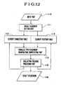
- Fig. 12 is a block diagram showing a general placement of an optimal element placement deciding apparatus for making decision as to whether or not a predetermined placement of numerous elements which correlate to one another is optimal by using a parallel processing type computer system which includes a plurality of CPUs.
- the apparatus shown in Fig. 12 has a structure closely similar to that of the apparatus shown in Fig. 1. In the case of the latter, information concerning the wiring relations and the positional relations among the elements in the optimal placement is outputted from the evaluation/decision processing part 15. In contrast, in the case of the apparatus shown in Fig. 12, the result of decision concerning whether or not a given element placement exhibits the local optimal value is outputted from the evaluation/decision processing part 115.
- connection table 112 the placement table 113, the parallel processing type placement computation part 114 and the evaluation/decision part 115 are of substantially same structures as those shown in Figs. 2, 3 and 4, and thus illustration and repeated description thereof will be unnecessary.
- decision can be made at a higher speed as to whether any given element placement exhibits the local optimal value.
- the processing speed can further be increased by adopting the multi-processor system with overhead being reduced.
Landscapes
- Engineering & Computer Science (AREA)
- Computer Hardware Design (AREA)
- Physics & Mathematics (AREA)
- Theoretical Computer Science (AREA)
- Architecture (AREA)
- Evolutionary Computation (AREA)
- Geometry (AREA)
- General Engineering & Computer Science (AREA)
- General Physics & Mathematics (AREA)
- Design And Manufacture Of Integrated Circuits (AREA)
Applications Claiming Priority (2)
| Application Number | Priority Date | Filing Date | Title |
|---|---|---|---|
| JP1062215A JPH02242474A (ja) | 1989-03-16 | 1989-03-16 | 素子配置最適化方法及び装置並びに最適配置判定方法及び装置 |
| JP62215/89 | 1989-03-16 |
Publications (2)
| Publication Number | Publication Date |
|---|---|
| EP0388794A2 true EP0388794A2 (fr) | 1990-09-26 |
| EP0388794A3 EP0388794A3 (fr) | 1991-11-06 |
Family
ID=13193703
Family Applications (1)
| Application Number | Title | Priority Date | Filing Date |
|---|---|---|---|
| EP19900104903 Withdrawn EP0388794A3 (fr) | 1989-03-16 | 1990-03-15 | Méthode et appareil pour optimiser le placement d'éléments et décider du placement optimal d'éléments |
Country Status (3)
| Country | Link |
|---|---|
| US (1) | US5144563A (fr) |
| EP (1) | EP0388794A3 (fr) |
| JP (1) | JPH02242474A (fr) |
Cited By (1)
| Publication number | Priority date | Publication date | Assignee | Title |
|---|---|---|---|---|
| EP0538035A3 (fr) * | 1991-10-15 | 1994-12-28 | Fujitsu Ltd |
Families Citing this family (55)
| Publication number | Priority date | Publication date | Assignee | Title |
|---|---|---|---|---|
| JPH04155584A (ja) * | 1990-10-19 | 1992-05-28 | Agency Of Ind Science & Technol | 組合せ最適化装置 |
| JP2575564B2 (ja) * | 1991-03-05 | 1997-01-29 | インターナショナル・ビジネス・マシーンズ・コーポレイション | 自動マクロ最適順序化方法 |
| JP2893144B2 (ja) * | 1991-06-10 | 1999-05-17 | 工業技術院長 | 組合せ最適化装置 |
| US5315534A (en) * | 1991-06-25 | 1994-05-24 | Unisys Corporation | Computer process for interconnecting logic circuits utilizing softwire statements |
| US5485396A (en) * | 1991-06-28 | 1996-01-16 | Vlsi Technology, Inc. | Symbolic routing guidance for wire networks in VLSI circuits |
| JPH05128142A (ja) * | 1991-11-08 | 1993-05-25 | Nkk Corp | 準最適解の探索方法 |
| JPH0812676B2 (ja) * | 1991-12-24 | 1996-02-07 | 工業技術院長 | 組合せ最適化装置 |
| JP3479538B2 (ja) * | 1991-12-26 | 2003-12-15 | テキサス インスツルメンツ インコーポレイテツド | 半導体集積回路を製作する方法 |
| JP3220250B2 (ja) * | 1992-01-09 | 2001-10-22 | 株式会社東芝 | セル自動配置方法 |
| EP0643855A1 (fr) * | 1992-06-04 | 1995-03-22 | Xilinx, Inc. | Methode de commande par temporisation pour l'implantation d'un circuit d'utilisateur sur un dispositif de circuit integre programmable |
| US5648913A (en) * | 1993-03-29 | 1997-07-15 | Xilinx, Inc. | Frequency driven layout system and method for field programmable gate arrays |
| JPH06332983A (ja) * | 1993-05-20 | 1994-12-02 | Mitsubishi Electric Corp | 部品配置最適化方法 |
| JP2922404B2 (ja) * | 1993-11-15 | 1999-07-26 | 富士通株式会社 | 集積回路の配置決定方法 |
| US6155725A (en) * | 1994-04-19 | 2000-12-05 | Lsi Logic Corporation | Cell placement representation and transposition for integrated circuit physical design automation system |
| US5963975A (en) * | 1994-04-19 | 1999-10-05 | Lsi Logic Corporation | Single chip integrated circuit distributed shared memory (DSM) and communications nodes |
| US5557533A (en) * | 1994-04-19 | 1996-09-17 | Lsi Logic Corporation | Cell placement alteration apparatus for integrated circuit chip physical design automation system |
| US5914887A (en) * | 1994-04-19 | 1999-06-22 | Lsi Logic Corporation | Congestion based cost factor computing apparatus for integrated circuit physical design automation system |
| US5495419A (en) * | 1994-04-19 | 1996-02-27 | Lsi Logic Corporation | Integrated circuit physical design automation system utilizing optimization process decomposition and parallel processing |
| US5875117A (en) * | 1994-04-19 | 1999-02-23 | Lsi Logic Corporation | Simultaneous placement and routing (SPAR) method for integrated circuit physical design automation system |
| US6493658B1 (en) | 1994-04-19 | 2002-12-10 | Lsi Logic Corporation | Optimization processing for integrated circuit physical design automation system using optimally switched fitness improvement algorithms |
| US5815403A (en) * | 1994-04-19 | 1998-09-29 | Lsi Logic Corporation | Fail-safe distributive processing method for producing a highest fitness cell placement for an integrated circuit chip |
| US5617328A (en) * | 1994-05-23 | 1997-04-01 | Winbond Electronics Corporation | Automatic code pattern generator for repetitious patterns in an integrated circuit layout |
| US5535134A (en) * | 1994-06-03 | 1996-07-09 | International Business Machines Corporation | Object placement aid |
| US5590063A (en) * | 1994-07-05 | 1996-12-31 | Motorola, Inc. | Optimization method using parallel processors |
| US5856927A (en) * | 1995-05-01 | 1999-01-05 | Vlsi Technology, Inc. | Method for automatically routing circuits of very large scale integration (VLSI) |
| US5870312A (en) * | 1996-06-28 | 1999-02-09 | Lsi Logic Corporation | Advanced modular cell placement system with dispersion-driven levelizing system |
| US6067409A (en) * | 1996-06-28 | 2000-05-23 | Lsi Logic Corporation | Advanced modular cell placement system |
| US6026223A (en) * | 1996-06-28 | 2000-02-15 | Scepanovic; Ranko | Advanced modular cell placement system with overlap remover with minimal noise |
| US5892688A (en) * | 1996-06-28 | 1999-04-06 | Lsi Logic Corporation | Advanced modular cell placement system with iterative one dimensional preplacement optimization |
| US5812740A (en) * | 1996-06-28 | 1998-09-22 | Lsi Logic Corporation | Advanced modular cell placement system with neighborhood system driven optimization |
| US5808899A (en) * | 1996-06-28 | 1998-09-15 | Lsi Logic Corporation | Advanced modular cell placement system with cell placement crystallization |
| US5870311A (en) * | 1996-06-28 | 1999-02-09 | Lsi Logic Corporation | Advanced modular cell placement system with fast procedure for finding a levelizing cut point |
| US6030110A (en) * | 1996-06-28 | 2000-02-29 | Lsi Logic Corporation | Advanced modular cell placement system with median control and increase in resolution |
| US6085032A (en) * | 1996-06-28 | 2000-07-04 | Lsi Logic Corporation | Advanced modular cell placement system with sinusoidal optimization |
| US5914888A (en) * | 1996-06-28 | 1999-06-22 | Lsi Logic Corporation | Advanced modular cell placement system with coarse overflow remover |
| US5963455A (en) * | 1996-06-28 | 1999-10-05 | Lsi Logic Corporation | Advanced modular cell placement system with functional sieve optimization technique |
| US5831863A (en) * | 1996-06-28 | 1998-11-03 | Lsi Logic Corporation | Advanced modular cell placement system with wire length driven affinity system |
| US5867398A (en) * | 1996-06-28 | 1999-02-02 | Lsi Logic Corporation | Advanced modular cell placement system with density driven capacity penalty system |
| US5872718A (en) * | 1996-06-28 | 1999-02-16 | Lsi Logic Corporation | Advanced modular cell placement system |
| US5844811A (en) * | 1996-06-28 | 1998-12-01 | Lsi Logic Corporation | Advanced modular cell placement system with universal affinity driven discrete placement optimization |
| US5835381A (en) * | 1996-06-28 | 1998-11-10 | Lsi Logic Corporation | Advanced modular cell placement system with minimizing maximal cut driven affinity system |
| US5980093A (en) * | 1996-12-04 | 1999-11-09 | Lsi Logic Corporation | Integrated circuit layout routing using multiprocessing |
| US5875118A (en) * | 1997-02-11 | 1999-02-23 | Lsi Logic Corporation | Integrated circuit cell placement parallelization with minimal number of conflicts |
| US6263475B1 (en) | 1997-11-17 | 2001-07-17 | Matsushita Electric Industrial Co., Ltd. | Method for optimizing component placement in designing a semiconductor device by using a cost value |
| US6385760B2 (en) * | 1998-06-12 | 2002-05-07 | Monterey Design Systems, Inc. | System and method for concurrent placement of gates and associated wiring |
| US6324436B1 (en) | 1998-09-14 | 2001-11-27 | Fujitsu Limited | Method for optimizing cost of manufacturing memory arrays |
| US6321187B1 (en) | 1998-12-22 | 2001-11-20 | Hamilton Sundstrand Corporation | System reliability assessment tool |
| JP2000268073A (ja) | 1999-03-18 | 2000-09-29 | Matsushita Electric Ind Co Ltd | 素子配置の最適化方法 |
| US6836753B1 (en) | 2001-06-13 | 2004-12-28 | Cadence Design Systems, Inc. | Cone slack allocator for computing time budgets |
| WO2003067814A2 (fr) * | 2002-02-01 | 2003-08-14 | California Institute Of Technology | Routeur rapide et procede de routage rapide assiste par materiel |
| WO2004019219A2 (fr) * | 2002-08-21 | 2004-03-04 | California Institute Of Technology | Procede et dispositif pour placer un element |
| US7285487B2 (en) * | 2003-07-24 | 2007-10-23 | California Institute Of Technology | Method and apparatus for network with multilayer metalization |
| US20100003030A1 (en) * | 2006-03-24 | 2010-01-07 | Gilfedder Timothy H | Optimisation of passive optical networks |
| US8136084B2 (en) * | 2009-09-09 | 2012-03-13 | International Business Machines Corporation | Arranging through silicon vias in IC layout |
| US9406562B2 (en) | 2011-01-13 | 2016-08-02 | GlobalFoundries, Inc. | Integrated circuit and design structure having reduced through silicon via-induced stress |
Family Cites Families (10)
| Publication number | Priority date | Publication date | Assignee | Title |
|---|---|---|---|---|
| US4495559A (en) * | 1981-11-02 | 1985-01-22 | International Business Machines Corporation | Optimization of an organization of many discrete elements |
| US4577276A (en) * | 1983-09-12 | 1986-03-18 | At&T Bell Laboratories | Placement of components on circuit substrates |
| US4630219A (en) * | 1983-11-23 | 1986-12-16 | International Business Machines Corporation | Element placement method |
| US4686629A (en) * | 1984-05-10 | 1987-08-11 | Rca Corporation | Logic cell placement method in computer-aided-customization of universal arrays and resulting integrated circuit |
| JPS6293760A (ja) * | 1985-10-18 | 1987-04-30 | Nec Corp | 配置改良装置 |
| US4754408A (en) * | 1985-11-21 | 1988-06-28 | International Business Machines Corporation | Progressive insertion placement of elements on an integrated circuit |
| JPS62175869A (ja) * | 1986-01-30 | 1987-08-01 | Fujitsu Ltd | モジユ−ル配置決定処理方式 |
| JPS62219062A (ja) * | 1986-03-19 | 1987-09-26 | Fujitsu Ltd | マルチ・プロセツサ方式 |
| JPS62243071A (ja) * | 1986-04-16 | 1987-10-23 | Fujitsu Ltd | 並列配置改善方式 |
| JPS63121978A (ja) * | 1986-11-11 | 1988-05-26 | Fujitsu Ltd | 大規模組合せ問題の最適化処理装置 |
-
1989
- 1989-03-16 JP JP1062215A patent/JPH02242474A/ja active Pending
-
1990
- 1990-03-13 US US07/492,906 patent/US5144563A/en not_active Expired - Fee Related
- 1990-03-15 EP EP19900104903 patent/EP0388794A3/fr not_active Withdrawn
Non-Patent Citations (4)
| Title |
|---|
| 20TH DESIGN AUTOMATION CONFERENCE, PROC'83, pages 182-188, IEEE, New York, US; D.-J. CHYAN et al.: "A placement algorithm for array processors" * |
| 23RD ACM/IEEE DESIGN AUTOMATION CONF., 29th June - 2nd July 1986, pages 622-629, IEEE, New York, US; B.T. PREAS et al.: "Automatic placement. A review of current techniques" * |
| IEEE TRANS. ON COMPUTER-AIDED DESIGN, vol. CAD-2, no. 1, January 1983, pages 39-47, IEEE, New York, US; K. UEDA et al.: "A parallel processing approach for logic module placement" * |
| IEEE TRANS. ON COMPUTER-AIDED DESIGN, vol. CAD-6, no. 4, July 1987, pages 534-549, New York, US; S.A. KRAVITZ et al.: "Placement by simulated annealing on a multiprocessor" * |
Cited By (2)
| Publication number | Priority date | Publication date | Assignee | Title |
|---|---|---|---|---|
| EP0538035A3 (fr) * | 1991-10-15 | 1994-12-28 | Fujitsu Ltd | |
| US5475608A (en) * | 1991-10-15 | 1995-12-12 | Fujitsu Limited | System for designing a placement of a placement element |
Also Published As
| Publication number | Publication date |
|---|---|
| JPH02242474A (ja) | 1990-09-26 |
| EP0388794A3 (fr) | 1991-11-06 |
| US5144563A (en) | 1992-09-01 |
Similar Documents
| Publication | Publication Date | Title |
|---|---|---|
| EP0388794A2 (fr) | Méthode et appareil pour optimiser le placement d'éléments et décider du placement optimal d'éléments | |
| US5392429A (en) | Method of operating a multiprocessor computer to solve a set of simultaneous equations | |
| Akl | Parallel sorting algorithms | |
| Gebotys et al. | Optimal VLSI architectural synthesis: area, performance and testability | |
| EP0067304A2 (fr) | Réseau de calcul et méthode pour la planification physique de circuits intégrés à très grande échelle | |
| EP0950966B1 (fr) | Procédé automatisé d'acheminement pour un circuit logique | |
| Sawik | An exact approach for batch scheduling in flexible flow lines with limited intermediate buffers | |
| JPH04241072A (ja) | 配線経路探索装置及び配線経路探索方法 | |
| US5721953A (en) | Interface for logic simulation using parallel bus for concurrent transfers and having FIFO buffers for sending data to receiving units when ready | |
| CN111079078B (zh) | 面向结构网格稀疏矩阵的下三角方程并行求解方法 | |
| JPH06139212A (ja) | 分散記憶型並列計算機のためのデータ分割パタンの評価方法、それを用いた並列プログラム生成方法およびそのためのプログラム実行時間の推定方法 | |
| US20220164189A1 (en) | Systems and methods for improved mapping of computational loops on reconfigurable architectures | |
| US6557143B1 (en) | Computer aided design system and computer-readable medium storing a program for designing clock gated logic circuits and gated clock circuit | |
| EP0745945A2 (fr) | Dispositif pour la génération de courbe paramétrique | |
| US7131085B2 (en) | Distributed BDD reordering | |
| EP0424908B1 (fr) | Système et méthode pour la détermination de modèle de câblage | |
| US5842035A (en) | Parallel computer utilizing less memory by having first and second memory areas | |
| Bernhard | Computers: Computing at the speed limit: Computers 1000 times faster than today's supercomputers would benefit vital scientific applications | |
| EP1192570B1 (fr) | Simulation d'evenement d'un logique des circuits | |
| Merigot et al. | A pyramidal system for image processing | |
| CN116775283A (zh) | 一种gpgpu资源分配管理方法及系统 | |
| EP1061463B1 (fr) | Planification du temps non entier de simulation pour la simulation de signaux mixtes | |
| French | A simple placement and routing algorithm for a two-dimensional computational origami architecture | |
| Tanomaru et al. | An evolutionary method for automatic wire routing | |
| Li et al. | A double-layer placement algorithm for integrated circuit-based modules on printed circuit board |
Legal Events
| Date | Code | Title | Description |
|---|---|---|---|
| PUAI | Public reference made under article 153(3) epc to a published international application that has entered the european phase |
Free format text: ORIGINAL CODE: 0009012 |
|
| AK | Designated contracting states |
Kind code of ref document: A2 Designated state(s): DE FR GB |
|
| 17P | Request for examination filed |
Effective date: 19901127 |
|
| PUAL | Search report despatched |
Free format text: ORIGINAL CODE: 0009013 |
|
| AK | Designated contracting states |
Kind code of ref document: A3 Designated state(s): DE FR GB |
|
| 17Q | First examination report despatched |
Effective date: 19941201 |
|
| STAA | Information on the status of an ep patent application or granted ep patent |
Free format text: STATUS: THE APPLICATION HAS BEEN WITHDRAWN |
|
| 18W | Application withdrawn |
Withdrawal date: 19950601 |