EP0745945A2 - Dispositif pour la génération de courbe paramétrique - Google Patents
Dispositif pour la génération de courbe paramétrique Download PDFInfo
- Publication number
- EP0745945A2 EP0745945A2 EP96303941A EP96303941A EP0745945A2 EP 0745945 A2 EP0745945 A2 EP 0745945A2 EP 96303941 A EP96303941 A EP 96303941A EP 96303941 A EP96303941 A EP 96303941A EP 0745945 A2 EP0745945 A2 EP 0745945A2
- Authority
- EP
- European Patent Office
- Prior art keywords
- curve
- register
- generating device
- new
- parametric
- Prior art date
- Legal status (The legal status is an assumption and is not a legal conclusion. Google has not performed a legal analysis and makes no representation as to the accuracy of the status listed.)
- Ceased
Links
Images




Classifications
-
- G—PHYSICS
- G06—COMPUTING OR CALCULATING; COUNTING
- G06F—ELECTRIC DIGITAL DATA PROCESSING
- G06F17/00—Digital computing or data processing equipment or methods, specially adapted for specific functions
- G06F17/10—Complex mathematical operations
- G06F17/17—Function evaluation by approximation methods, e.g. inter- or extrapolation, smoothing, least mean square method
-
- G—PHYSICS
- G06—COMPUTING OR CALCULATING; COUNTING
- G06F—ELECTRIC DIGITAL DATA PROCESSING
- G06F17/00—Digital computing or data processing equipment or methods, specially adapted for specific functions
Definitions
- the present invention relates to a parametric curve generating device, which can be used to generate an outline font character utilized in the office automation equipment such as a computer or a printer, or an arbitrary parametric curve utilized in the field of CAD, designing etc.
- the division of the initial values (P 0 ...P 3 ) generates data of twice amount, of which one set (R 0 ...R 3 ) is saved in a stack and the other (Q 0 ...Q 3 ) is used as the initial values of the next division. This operation is repeated, and, if the data (Q 0 ...Q 3 ) converge at a certain point, the data (R 0 ...R 3 ) are used as the initial values for the next operation. If both data (Q 0 ...Q 3 ) and (R 0 ...R 3 ) converge, the data of the control points immediately previously saved in the stack are revived as the initial values for the next operation. All the operations are completed when the stack becomes empty. Through such process, there can be obtained a train of the developed drawn points of the Bezier curve, in continuous manner from P 0 to P 3 . s
- the operation of determining the middle point of two control points involves an addition and a division into 1/2. Since the 1/2 division can be achieved by a 1-bit shift to the right, an adder can achieve the addition and the 1/2 division by shifting the output of the adder to the right by a bit. If the data of the control points are of n bits, the result of the 1/2 division is given by the upper (n-1) bits of the result of addition. Also the carry-over output of the adder may be used as the uppermost bit of the result of the calculation.
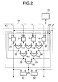
- Fig. 2 shows an example of a circuit of a parametric curve generating device that could be used for effecting the above-mentioned 1/2 division.
- the above-mentioned data (P 0 ...P 3 ) are respectively stored in registers 1 - 4.
- Adders 11 - 16 execute the 1/2 divisions, and the results of the operation (Q 0 ...Q 3 , R 0 ...R 3 ) are released to points 21 - 27 (Q 3 and R 0 are same and released to a point 24).
- Convergence discrimination circuits 31, 32 respectively determine
- the function of the above-explained parametric curve generating device is classified into three cases according to the state of convergence of the control points, namely a case where (Q 0 ...Q 3 ) do not converge, a case where (Q 0 ...Q 3 ) converge but (R 0 ...R 3 ) do not converge, and a case where (Q 0 ...Q 3 ) and ( R 0 ...R 3 ) both converge.
- Such function is controlled by an unrepresented control circuit.
- the data of each control point is data with a floating decimal point, consisting of an integral part of 1 o bits and a fractional part of 1 1 bits.
- the number 1 1 of bits of the fractional part has generally to be comparable with 1 0 .
- each of the registers 1 - 4 and the adders 11 - 16 of the above-explained parameter curve generating device has to have about 32 bits, so that the magnitude of the hardware becomes considerably large.
- the data bus 51 is required to have a width of 96 bits. The presence of a bus of such large width requires a large wiring area and is disadvantageous in forming this circuit into an LSI.
- One such embodiment provides a parametric curve generating device for generating an arbitrary parametric curve, comprising a first register for storing the coordinates of the control point of the curve; a 1/2 division circuit for dividing the control points, stored in the register, into two thereby forming control points of two curves; a second register for storing the control points of the two curves formed by the 1/2 division circuit; a stack memory for successively storing the control points of plural sets; and a discrimination circuit for determining whether or not to effect the division of the control points by the 1/2 division circuit, wherein a desired parametric curve is generated and released by repeating the 1/2 division on the control points given in advance to the first register.
- a third register may be positioned between the first and second registers and the stack memory and adapted to store the control points of a set.
- the set to be saved is once stored in the third register and then stored in the stack memory.
- control points of a temporarily saved set of the curve are transferred to the first register according to the result of discrimination by the discrimination circuit, the content of the third register is transferred.
- the dividing operation of the 1/2 division circuit and the transfer between the third register and the stack memory are simultaneously executed in parallel manner.
- the stack memory is so constructed as to read and write a control point at a time.
- the 1/2 division circuit is composed of three adders and the dividing operation of each control point is completed in three clock cycles.
- each of the registers and the stack memory is composed of an integral part and a fractional part.
- the generated curve is a Bezier curve.
- the above-mentioned Bezier curve belong to a two-dimensional space having x and y coordinates, and the above-mentioned registers and stack memory are provided for each of the x and y coordinates.
- the above-mentioned output means is a printer.
- the parametric curve generating device of the embodiments generates a desired parametric curve, by repeating a 1/2 dividing operation on the points of a parametric curve given to the first register and saving the data from the adders to the stack memory or reviving the data from the stack memory to the adders.
- the parametric curve generating device of one embodiment is capable of simultaneously executing the dividing operation of the control points of theparametric curve by the 1/2 division circuit and the saving/reviving operation of a set of the control points to or from the stack memory in parallel manner, through the use of the third register. Owing to this configuration, each 1/2 dividing operation can be conducted within 4 clock cycles in all cases, regardless of the state of convergence.
- Fig. 3 shows an example of the circuit embodying the present invention, wherein shown are registers 71 - 74 for storing the data (P 0 ...P 3 ) as in the registers 1 - 4 explained in the foregoing; adders 81 - 83 which are reduced in number from six to three in comparison with the configuration shown in Fig. 2; registers 91 - 97 which are increased in number in comparison with the configuration in Fig. 2; a stack memory 101; and a bus 111 connecting the stack memory 101 with the registers 72 - 74.
- This circuit is controlled by an unrepresented control circuit.
- P 0 is transferred as Q 0 to the register 91
- P 3 is transferred as R 3 to the register 97.
- the adder 81 adds the content of the register 92 and that of the register 94 and multiples by 1/2, and the obtained result is stored as Q 2 in the register 93.
- the adder 83 adds the contents of the registers 94 and 96 and multiplies by 1/2, and the obtained result is stored as R 1 in the register 95.
- the adder 82 adds the contents of the register 93 and 95 and multiples by 1/2, and the obtained result is stored as Q 3 (F 0 ) in the register 94.
- the 1/2 division as in Fig. 2 can be executed within three clock cycles.
- the convergence discrimination circuits 121, 122 discriminate whether (Q 0 ...Q 3 ) and (R 0 ...R 3 ) are in the converged state, and the process varies according to the result of the discrimination.
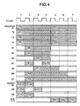
- Fig. 4 shows a case where (Q 0 ...Q 3 ) do not converge.
- the selector 131 is so switched that (Q 1 ...Q 3 ) are stored in the registers 72 - 74 at the start of the next cycle, that is, at the start of a fifth cycle.
- the content of the register 71, being Q 0 remains unchanged.
- (R 1 ...R 3 ) are saved in succession in the stack memory 101 through the bus 111, in fifth, sixth and seventh cycles.
- the next 1/2 division cannot be started until the completion of the storage. Consequently there are required 7 cycles in this case.
- Fig. 5 shows a case where (Q 0 ...Q 3 ) converge but (R 0 ...R 3 ) do not converge.
- Q 0 is released and the selector 131 is so switched that (R 0 ...R 2 ) are stored in the registers 71 - 73.
- (R 0 ...R 2 ) are stored in the registers 71 - 73 at the start of the fifth cycle.
- the content of the register 74 being R 3 , remains unchanged. In this case there are required 4 cycles, because the contents of the registers 71 - 74 are fixed at the start of the fifth cycle so that the aforementioned operations of the first cycle and thereafter can be started from the fifth cycle.
- Fig. 6 shows a case where (Q 0 ...Q 3 ) and (R 0 ...R 3 ) both converge.
- Q 0 and R 3 are released, and the selector 131 is so switched that the data of the control points can be revived in the fifth, sixth and seventh cycles and that the content of the register 97 can be transferred to the register 71.
- the data (P 1 ', P 2 ', P 3 ') of three control points are revived from the stack memory 101 to the registers 72 - 74 through the bus 111, in the fifth, sixth and seventh cycles.
- the content (P 0 ') of the register 97 is stored in the register 71 through the selector 131, at the start of the fifth cycle. In this case there are required 7 cycles, as the contents of the registers 71 - 74 are fixed at the start of the eighth cycle.
- the width of the data port of the stack memory 101 and of the bus 111 is 32 bits, so that it is more suitable for LSI formation.
- the clock cycle has to be set as follows, disregarding the data transfer time:
- the clock cycle in Fig. 3 can be made as about 1/4 of the clock cycle in Fig. 2. Consequently, in comparison with the circuit shown in Fig. 2, the circuit in Fig. 3 can process with a comparable speed in case (Q 0 ...Q 3 ) converge but (R 0 ...R 3 ) do not converge, but is slower by the time required for the cycles for transfer with the stack memory 101 in other cases.
- Fig. 7 shows another embodiment of the present invention, wherein components equivalent in function and position to those in Fig. 3 are represented by primed corresponding numbers. Registers 141 - 143 alone are added to the configuration shown in Fig. 3, so that the increase in the magnitude of circuitry in this embodiment is minimal.
- adders 81' - 83' effect calculations (P 0 + P 1 )/2, (P 1 + P 2 )/2 and (P 2 + P 3 )/2, of which results Q 1 , S, R 2 are respectively stored in the registers 92', 94', 96'.
- P 0 is transferred as Q 0 to the register 91'
- P 3 is transferred as R 3 to the register 97'.
- the adder 81' adds the contents Q 1 , S of the registers 92', 94' and multiplies by 1/2, and the obtained result Q 2 is stored in the register 93'. Also the adder 83' adds the contents S, R 2 of the registers 94', 96' and multiplies by 1/2, and the obtained result R 1 is stored in the register 95'.
- the 1/2 division as in Fig. 2 can be executed within three clock cycles.
- the convergence discrimination circuits 121', 122' discriminate whether (Q 0 ...Q 3 ) and (R 0 ...R 3 ) are in the converged state, and the process varies according to the result of the discrimination.
- Fig. 8 shows a case where (Q 0 ...Q 3 ) do not converge.
- the selector 131' is so switched that (Q 1 ...Q 3 ) are stored in the registers 72' - 74' at the start of the fifth cycle, and (R 1 ...R 3 ) are stored in the registers 141 - 143 at the start of the fifth cycle.
- (Q 1 ...Q 3 ) are stored in the registers 72' - 74' in the fifth cycle.
- the content of the register 71, being Q 0 remains unchanged.
- (R 1 ...R 3 ) are stored in the registers 141 - 143.
- the contents of the registers 141 - 143 are saved in succession in the stack memory 101', but the contents of the registers 141 - 143 remain unchanged.
- Fig. 9 shows a case where (Q 0 ...Q 3 ) converge but (R 0 ...R 3 ) do not converge.
- Q 0 is released and the selector 131' is so switched that (R 0 ...R 2 ) are stored in the registers 71' - 73'.
- (R 0 ...R 2 ) are stored in the registers 71' - 73' at the start of the fifth cycle.
- the content of the register 74', being R 3 remains unchanged.
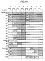
- Fig. 10 shows a case where (Q 0 ...Q 3 ) and (R 0 ... R 3 ) both converge.
- the convergence discrimination circuits 121', 122', Q 0 and R 0 are released, and the selector 131' is so switched that the contents (P 1 ', P 2 ', P 3 ') of the registers 141 - 143 are transferred to the registers 72' - 74' and the content (P 0 ') of the register 97' is transferred to the register 71' in the fifth cycle.
- the contents of the registers 141 - 143 are transferred to the registers 72' - 74'.
- the contents of the registers 141 - 143 are same as those immediately previously saved in the stack memory 101'. Also at the start of the fifth cycle, the content of the register 74' is stored in the register 71' through the selector 131'. Then, in the fifth, sixth and seventh cycles, the data (P 1 ", P 2 ", P 3 ") present in the second position from the top of the stack memory are revived in succession to the registers 141 - 143 from the stack memory 101', through the bus 111'. Also a preceding set of data is brought to the top of the stack memory.
- the content of the registers 141 - 143 always coincides with the data of a set at the top of the stack memory 101', after each 1/2 dividing operation.
- the content of the registers 141 - 143 may be used for reviving the data of the control points in the registers 72' - 74' without waiting for a bus cycle, even when there continues the situation where (Q 0 ...Q 3 ) and (R 0 ...R 3 ) both converge.
- the bus cycle occurs always in the fifth, sixth and seventh cycles.
- the transfer cycle 2) occurs always at the start of the fifth cycle.
- the data required for the next operation are fixed in the registers 71' - 74' at the start of the fifth cycle.
- the 1/2 dividing operation can be executed in independent and continuous manner, utilizing the data in the registers 71' - 74'.
- the number of necessary clock cycles it is defined as 4 clock cycles, utilizing the above-mentioned pipeline operation.
- a clock cycle can be selected comparable to that in the circuit shown in Fig. 3.
- FIG. 3 and 7 employ the registers 91, 97, 91', 97' for the purpose of simplicity, but these registers may be dispensed with. In such case the registers 91, 91', 97, 97' are replaced by the registers 71, 71', 74, 74' respectively.
- the parametric curve generating device of the present embodiment is capable, by the entry of outline font data stored in a memory, of deriving control points for developing a curve, developing the curve based on thus derived control points and providing thus developed curve by an unrepresented printer or an unrepresented display device.
- the parametric curve generating device of the present invention is capable of high-speed development of a Bezier curve with a limited magnitude of hardware. Also it is particularly suitable for LSI formation, because of the reduced bus width.
- the embodiments above further include means (not shown) for processing the derived control points to generate a display of a curve, for example on a display device (not shown) or on a paper copy.
Landscapes
- Engineering & Computer Science (AREA)
- Physics & Mathematics (AREA)
- General Physics & Mathematics (AREA)
- Theoretical Computer Science (AREA)
- Mathematical Physics (AREA)
- Data Mining & Analysis (AREA)
- Computational Mathematics (AREA)
- Mathematical Analysis (AREA)
- Mathematical Optimization (AREA)
- Pure & Applied Mathematics (AREA)
- Software Systems (AREA)
- General Engineering & Computer Science (AREA)
- Databases & Information Systems (AREA)
- Algebra (AREA)
- Image Generation (AREA)
- Complex Calculations (AREA)
Applications Claiming Priority (2)
| Application Number | Priority Date | Filing Date | Title |
|---|---|---|---|
| JP134192/95 | 1995-05-31 | ||
| JP7134192A JPH08329261A (ja) | 1995-05-31 | 1995-05-31 | パラメータ曲線発生器 |
Publications (2)
| Publication Number | Publication Date |
|---|---|
| EP0745945A2 true EP0745945A2 (fr) | 1996-12-04 |
| EP0745945A3 EP0745945A3 (fr) | 1999-04-14 |
Family
ID=15122592
Family Applications (1)
| Application Number | Title | Priority Date | Filing Date |
|---|---|---|---|
| EP96303941A Ceased EP0745945A3 (fr) | 1995-05-31 | 1996-05-31 | Dispositif pour la génération de courbe paramétrique |
Country Status (5)
| Country | Link |
|---|---|
| US (1) | US5900884A (fr) |
| EP (1) | EP0745945A3 (fr) |
| JP (1) | JPH08329261A (fr) |
| KR (1) | KR100202044B1 (fr) |
| TW (1) | TW311998B (fr) |
Cited By (3)
| Publication number | Priority date | Publication date | Assignee | Title |
|---|---|---|---|---|
| US5717905A (en) * | 1994-12-15 | 1998-02-10 | Kao Corporation | CAD system and bezier-curve data converting apparatus and method thereof in said CAD system |
| WO2003015031A1 (fr) * | 2001-08-06 | 2003-02-20 | Sharp Kabushiki Kaisha | Methode, dispositif et programme d'approximation de courbe |
| AU768344B2 (en) * | 2000-02-10 | 2003-12-11 | Canon Kabushiki Kaisha | Animating character outlines |
Families Citing this family (11)
| Publication number | Priority date | Publication date | Assignee | Title |
|---|---|---|---|---|
| US6067094A (en) * | 1998-04-07 | 2000-05-23 | Adobe Systems Incorporated | Brushstroke envelopes |
| JP3270928B2 (ja) * | 1999-09-30 | 2002-04-02 | コナミ株式会社 | フィールドマップ生成方法、ビデオゲームシステム、及び記録媒体 |
| US7212205B2 (en) | 2002-11-12 | 2007-05-01 | Matsushita Electric Industrial Co., Ltd. | Curved surface image processing apparatus and curved surface image processing method |
| US7015917B2 (en) * | 2003-07-18 | 2006-03-21 | Matsushita Electric Industrial Co., Ltd. | Curved surface subdivision apparatus |
| JP4866013B2 (ja) * | 2005-03-31 | 2012-02-01 | 富士通株式会社 | 文字画像生成プログラム、そのシステム、及びその方法 |
| JP5247671B2 (ja) * | 2009-12-22 | 2013-07-24 | ルネサスエレクトロニクス株式会社 | 表示データ補正装置、及び、それを使用する表示パネルドライバ、表示装置 |
| US9019277B2 (en) | 2010-06-30 | 2015-04-28 | Panasonic Intellectual Property Management Co., Ltd. | Curve-dividing device, curve-dividing method, curve-dividing program and integrated circuit |
| JP5767516B2 (ja) | 2010-10-08 | 2015-08-19 | キヤノン株式会社 | 画像処理装置、画像処理方法、及びプログラム |
| US9224219B2 (en) * | 2012-12-21 | 2015-12-29 | Citrix Systems, Inc. | Systems and methods for presenting a free-form drawing |
| US10347016B2 (en) * | 2016-01-12 | 2019-07-09 | Monotype Imaging Inc. | Converting font contour curves |
| US10936792B2 (en) | 2017-12-21 | 2021-03-02 | Monotype Imaging Inc. | Harmonizing font contours |
Family Cites Families (9)
| Publication number | Priority date | Publication date | Assignee | Title |
|---|---|---|---|---|
| DE68927786D1 (de) * | 1988-06-29 | 1997-04-03 | Fujitsu Ltd | Verfahren und Gerät zur Annäherung einer Kurve mit einer polygonalen Linie |
| US5023828A (en) * | 1988-07-20 | 1991-06-11 | Digital Equipment Corporation | Microinstruction addressing in high-speed CPU |
| US4989210A (en) * | 1988-08-30 | 1991-01-29 | Unisys Corporation | Pipelined address check bit stack controller |
| US5241654A (en) * | 1988-12-28 | 1993-08-31 | Kabushiki Kaisha Toshiba | Apparatus for generating an arbitrary parameter curve represented as an n-th order Bezier curve |
| JPH02176879A (ja) * | 1988-12-28 | 1990-07-10 | Toshiba Corp | パラメータ曲線発生器 |
| JPH03127186A (ja) * | 1989-10-12 | 1991-05-30 | Mitsubishi Electric Corp | 描画方式 |
| JP2734711B2 (ja) * | 1990-01-12 | 1998-04-02 | 日本電気株式会社 | 曲線発生装置 |
| JPH0458378A (ja) * | 1990-06-28 | 1992-02-25 | Mitsubishi Heavy Ind Ltd | ベジエ曲線を分割して展開する方法 |
| US5128887A (en) * | 1991-01-31 | 1992-07-07 | Hewlett-Packard Company | Numerical accuracy indicator for rounded numeric value display method |
-
1995
- 1995-05-31 JP JP7134192A patent/JPH08329261A/ja active Pending
-
1996
- 1996-05-28 TW TW085106343A patent/TW311998B/zh active
- 1996-05-29 US US08/657,033 patent/US5900884A/en not_active Expired - Fee Related
- 1996-05-30 KR KR1019960018720A patent/KR100202044B1/ko not_active Expired - Fee Related
- 1996-05-31 EP EP96303941A patent/EP0745945A3/fr not_active Ceased
Cited By (3)
| Publication number | Priority date | Publication date | Assignee | Title |
|---|---|---|---|---|
| US5717905A (en) * | 1994-12-15 | 1998-02-10 | Kao Corporation | CAD system and bezier-curve data converting apparatus and method thereof in said CAD system |
| AU768344B2 (en) * | 2000-02-10 | 2003-12-11 | Canon Kabushiki Kaisha | Animating character outlines |
| WO2003015031A1 (fr) * | 2001-08-06 | 2003-02-20 | Sharp Kabushiki Kaisha | Methode, dispositif et programme d'approximation de courbe |
Also Published As
| Publication number | Publication date |
|---|---|
| KR100202044B1 (ko) | 1999-06-15 |
| JPH08329261A (ja) | 1996-12-13 |
| KR960042420A (ko) | 1996-12-21 |
| US5900884A (en) | 1999-05-04 |
| EP0745945A3 (fr) | 1999-04-14 |
| TW311998B (fr) | 1997-08-01 |
Similar Documents
| Publication | Publication Date | Title |
|---|---|---|
| EP0745945A2 (fr) | Dispositif pour la génération de courbe paramétrique | |
| US3304418A (en) | Binary-coded decimal adder with radix correction | |
| US5226171A (en) | Parallel vector processing system for individual and broadcast distribution of operands and control information | |
| EP0411491B1 (fr) | Procédé et appareil pour l'exécution des divisions utilisant un multiplieur à format rectangulaire | |
| US5025405A (en) | Method of interpolating pixel values | |
| EP0388794A2 (fr) | Méthode et appareil pour optimiser le placement d'éléments et décider du placement optimal d'éléments | |
| US4228498A (en) | Multibus processor for increasing execution speed using a pipeline effect | |
| KR930006536A (ko) | 문자/도형 발생 장치 및 정보 처리 장치 | |
| EP0321089A2 (fr) | Système de stockage dans un tampon de données numériques | |
| JPH053032B2 (fr) | ||
| EP0088544B1 (fr) | Système de traitement de vecteur à opération continue, limitée par indexage | |
| US4381550A (en) | High speed dividing circuit | |
| US3964028A (en) | System and method for evaluating paging behavior | |
| US5727200A (en) | Parallel merge sorting apparatus with an accelerated section | |
| EP0437379B1 (fr) | Générateur de courbes | |
| US5339267A (en) | Preprocessor of division device employing high radix division system | |
| US20050229124A1 (en) | Distributed BDD reordering | |
| JP2518293B2 (ja) | デ−タフロ−プロセツサ | |
| KR970004107B1 (ko) | 파라미터곡선발생기 | |
| JPS58129653A (ja) | 乗算方式 | |
| US5163129A (en) | Method for expediting the rendering of figures in a move-draw language | |
| EP0256488B1 (fr) | Méthode d'interpolation de valeurs de pixel | |
| US5381380A (en) | Divide circuit having high-speed operating capability | |
| EP1187044A2 (fr) | Génération optimisée de hardware à partir de programmes sources avec multiplications | |
| JPH02171914A (ja) | 印刷データ生成装置 |
Legal Events
| Date | Code | Title | Description |
|---|---|---|---|
| PUAI | Public reference made under article 153(3) epc to a published international application that has entered the european phase |
Free format text: ORIGINAL CODE: 0009012 |
|
| AK | Designated contracting states |
Kind code of ref document: A2 Designated state(s): DE FR GB |
|
| K1C3 | Correction of patent application (complete document) published |
Effective date: 19961204 |
|
| PUAL | Search report despatched |
Free format text: ORIGINAL CODE: 0009013 |
|
| AK | Designated contracting states |
Kind code of ref document: A3 Designated state(s): DE FR GB |
|
| RHK1 | Main classification (correction) |
Ipc: G06T 11/20 |
|
| 17P | Request for examination filed |
Effective date: 19990830 |
|
| 17Q | First examination report despatched |
Effective date: 20010308 |
|
| GRAG | Despatch of communication of intention to grant |
Free format text: ORIGINAL CODE: EPIDOS AGRA |
|
| STAA | Information on the status of an ep patent application or granted ep patent |
Free format text: STATUS: THE APPLICATION HAS BEEN REFUSED |
|
| 18R | Application refused |
Effective date: 20020913 |