EP0389847A2 - Circuit - Google Patents
Circuit Download PDFInfo
- Publication number
- EP0389847A2 EP0389847A2 EP90104513A EP90104513A EP0389847A2 EP 0389847 A2 EP0389847 A2 EP 0389847A2 EP 90104513 A EP90104513 A EP 90104513A EP 90104513 A EP90104513 A EP 90104513A EP 0389847 A2 EP0389847 A2 EP 0389847A2
- Authority
- EP
- European Patent Office
- Prior art keywords
- circuit arrangement
- circuit
- voltage
- arrangement according
- switching
- Prior art date
- Legal status (The legal status is an assumption and is not a legal conclusion. Google has not performed a legal analysis and makes no representation as to the accuracy of the status listed.)
- Granted
Links
Images





Classifications
-
- H—ELECTRICITY
- H05—ELECTRIC TECHNIQUES NOT OTHERWISE PROVIDED FOR
- H05B—ELECTRIC HEATING; ELECTRIC LIGHT SOURCES NOT OTHERWISE PROVIDED FOR; CIRCUIT ARRANGEMENTS FOR ELECTRIC LIGHT SOURCES, IN GENERAL
- H05B41/00—Circuit arrangements or apparatus for igniting or operating discharge lamps
- H05B41/14—Circuit arrangements
- H05B41/16—Circuit arrangements in which the lamp is fed by DC or by low-frequency AC, e.g. by 50 cycles/sec AC, or with network frequencies
-
- H—ELECTRICITY
- H05—ELECTRIC TECHNIQUES NOT OTHERWISE PROVIDED FOR
- H05B—ELECTRIC HEATING; ELECTRIC LIGHT SOURCES NOT OTHERWISE PROVIDED FOR; CIRCUIT ARRANGEMENTS FOR ELECTRIC LIGHT SOURCES, IN GENERAL
- H05B41/00—Circuit arrangements or apparatus for igniting or operating discharge lamps
- H05B41/14—Circuit arrangements
- H05B41/26—Circuit arrangements in which the lamp is fed by power derived from DC by means of a converter, e.g. by high-voltage DC
- H05B41/28—Circuit arrangements in which the lamp is fed by power derived from DC by means of a converter, e.g. by high-voltage DC using static converters
-
- Y—GENERAL TAGGING OF NEW TECHNOLOGICAL DEVELOPMENTS; GENERAL TAGGING OF CROSS-SECTIONAL TECHNOLOGIES SPANNING OVER SEVERAL SECTIONS OF THE IPC; TECHNICAL SUBJECTS COVERED BY FORMER USPC CROSS-REFERENCE ART COLLECTIONS [XRACs] AND DIGESTS
- Y10—TECHNICAL SUBJECTS COVERED BY FORMER USPC
- Y10S—TECHNICAL SUBJECTS COVERED BY FORMER USPC CROSS-REFERENCE ART COLLECTIONS [XRACs] AND DIGESTS
- Y10S315/00—Electric lamp and discharge devices: systems
- Y10S315/05—Starting and operating circuit for fluorescent lamp
Definitions
- the invention relates to a circuit arrangement for the high-frequency operation of one or more low-pressure discharge lamps connected in parallel to one another according to the preamble of the main claim.
- Such circuit arrangements are known per se (DE-OS 36 23 749, DE-OS 36 11 611 and DE-OS 37 00 421). Although these circuits can feed a low-pressure discharge lamp at a high frequency and meet the existing regulations regarding the form of mains current, they still require a considerable amount of components.
- the desired circuit effects in the known circuits are based on the function of a push-pull output stage in conjunction with at least four diodes and three capacitors.
- the object of the invention is to provide a circuit arrangement for the high-frequency operation of low-pressure discharge lamps, which manages with a minimum of components.
- the circuit arrangement according to the invention manages with fewer components than the known circuit arrangements, since the high-frequency generator is constructed as a single-ended high-frequency generator which has only one switching transistor, one switching inductor, one oscillating capacitor and two diodes.
- the high-frequency generator is constructed as a single-ended high-frequency generator which has only one switching transistor, one switching inductor, one oscillating capacitor and two diodes.
- an advantageous embodiment of the circuit arrangement according to the invention is characterized in that the active harmonic filter has a series inductance, a pump capacitor and two decoupling diodes.
- the switching transistor switches the pump capacitor between the series inductance and one of the decoupling diodes against the reference potential.
- the mains current is modulated sinusoidally with every lamp cycle.
- an amount of energy proportional to the respective instantaneous value of the line voltage is drawn from the network and supplied to the smoothing capacitor via one of the two decoupling diodes. This ensures a sinusoidally modulated mains current consumption through the harmonic filter.
- the pump capacitor is connected from the collector or drain terminal of the switching transistor via the one decoupling diode in parallel to the switching inductance and the other decoupling diode, with the resoiling of the voltage at the switching transistor nance behavior, determined by the switching inductance and the pump capacitor, is predetermined. It is also advantageous if the single-ended high-frequency generator is operated at the resonance frequency, determined by the switching inductance and the pump capacitor. This switching of the switching transistor creates an advantageous switch-off relief network.
- the pump capacitor is connected in parallel with the switching inductance via the two decoupling diodes, so that the amplitude of the negative current half-wave in the lamp is reduced and the crest factor of the lamp current is improved.
- the switching transistor is controlled by an electronic control circuit which advantageously has an electronic oscillator and a pulse width modulator.
- the electronic control circuit forms an electronic interface.
- the electronic oscillator and the pulse width modulator can be started and stopped electronically and their pulse width or frequency can be set via an electronic control signal. This creates an interface that is desirable for various user options.
- a further improved circuit arrangement enables starting with preheated electrodes and also offers corresponding safety functions and protection against overvoltage and overcurrents, such as those e.g. if a lamp fails.
- the switching inductance has two additional secondary windings which, depending on the lamp voltage, are switched to the respective heating filament of the lamp via a thyristor and heat the heating filament with their voltages.
- control electronics are designed such that each time the circuit is started up for the first time, the switching frequency of the single-ended high-frequency converter is first increased, in order then to be reduced continuously to the actual clock frequency in the 1/10 second range, so that an increased heating current is available for each new start-up.
- both the voltage at the collector of the switching transistor and the electronics self-supply voltage are detected in their respective levels and, in the event of overvoltage, by firing a thyristor used to short-circuit the start-up circuit and the control of the switching transistor. This enables the circuit to be shut down safely.
- an electronic supply voltage is derived from the rectified mains voltage via a series resistor, which is switched through with a thyristor when the maximum permissible limit value for the electronic supply voltage is reached, so that the thyristor can hold itself over the electronic supply current.
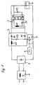
- FIG. 1 shows the basic structure of the circuit arrangement for the high-frequency operation of a low-pressure discharge lamp LL1.
- the circuit arrangement includes a high-frequency filter 1, a mains rectifier 2, a single-ended high-frequency generator with a switching transistor T1 and an electronic control circuit 6 for controlling the single-ended high-frequency generator, as well as a smoothing capacitor 4 and an active harmonic filter 3.
- the harmonic filter 3 consists of a series inductor L2, a pump capacitor C2, the decoupling diodes D6 and D5 and the switching transistor T1 of the single-ended high-frequency generator.
- the high-frequency filter 1 is located at the input of the network, followed by the network rectifier 2 in a 2-pulse, uncontrolled bridge circuit.
- the single-ended high-frequency generator operated via an electronic control circuit 6 consists of the switching transistor T1, a switching inductance L1 and an oscillating capacitor C1.
- the electrodes of the lamp LL1 are connected on one side E1, H1 to the switching inductance L1, and the smoothing capacitor CO and on the other side E2, H2 to the oscillating capacitor C1.
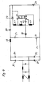
- the electrodes of the heating circuits H1 and H2 can, as shown in FIG. 2, be connected via a heating capacitor C3; or a heating winding can be connected separately with E1-H1 and E2-H2 as part winding of the switching inductance L1, as shown in FIG. 4.
- the high-frequency operated single-ended converter supplies a portion of the positive current half-wave of the lamp via the oscillating capacitor C1 from the positive pole of the smoothing capacitor C0 when the switching transistor is conductive.
- the switching inductance L1 charges an energy portion proportional to the switch-on time of the switching transistor T1.
- an oscillating circuit is formed via the lamp, the resonance capacitor C1 and the switching inductance L1, which initially produces the negative current half-wave of the lamp with the same current direction in the switching inductance L1 and then when the current direction is reversed in the switching inductance L1 by discharging the oscillation capacitor C1 the positive current half-wave generated in the lamp.
- the smoothing capacitor CO is decoupled from the mains voltage via the decoupling diode D6.
- the circuit arrangement also has an active harmonic filter, which consists of the series inductor L2 located in the positive line, the pump capacitor C2 and the decoupling diodes D5 and D6.
- the pump capacitor C2 When the switching transistor T1 is switched “on”, the pump capacitor C2 is charged via the series inductor L2 up to the voltage level at the smoothing capacitor C0.
- the charging current is taken from the network.
- An energy part is thus stored in the longitudinal inductance L2 and is emitted to the single-ended high-frequency generator, the lamp and the smoothing capacitor CO after charging of the pump capacitor C2 has ended.
- the amount of energy per cycle is proportional to the voltage time area at the series inductor L2 and is determined by the difference between the instantaneous mains voltage values and the voltage at the pump capacitor C2, which is present in negative polarity due to the preceding "switch-off" cycle. certainly.
- the line current is modulated sinusoidally with each lamp cycle.
- the energy output of the longitudinal inductor L2 takes place by demagnetizing the longitudinal inductor L2.
- the voltage at the series inductor L2 reverses and reaches a voltage value equal to the difference between the voltage at the smoothing capacitor C0 and the respective instantaneous value of the mains voltage.
- a second phase begins in the action of the pump capacitor C2.
- the current flowing in the switching inductance L1 commutates from the switching transistor T1 partly to the pump capacitor C2 as discharge and reversing current and partly to the oscillating capacitor C1 and the low-pressure discharge lamp, which thus receives its negative current half-wave.
- the pump capacitor C2 thus acts as a switch-off relief network for the switching transistor T1.
- the voltage at the collector or drain connection of the switching transistor T1 can therefore only change as quickly as the pump capacitor C2 with its resonance frequency, determined by the capacitance of the pump capacitor C2 and the inductance value of the switching inductance L1, is recharged. This limitation of the rise in voltage at the switching transistor T1 considerably reduces its turn-off losses.
- the negative current half-wave in the oscillating capacitor C1 and the low-pressure discharge lamp LL1 is reduced by the current part which commutates from the switching inductance L1 as the charge-reversal current to the pump capacitor C2. This improves the crest factor of the lamp current and thus the service life of the low-pressure discharge lamp.
- the electronic control circuit 6 of the switching transistor consists of an electronic oscillator and a pulse width modulator, which can be started and stopped electronically and whose pulse width or frequency via an electroni cal control signal is adjustable. This enables an electronic interface to be implemented, as is required for various user options.
- the circuit part assigned to the low-pressure discharge lamp LL1 consists of the decoupling diodes D5.1 and D6.1, the switching inductance L1.1, the oscillating capacitor C1.1. and the heating capacitor C3.1.
- the circuit part assigned to the low-pressure discharge lamp LL2 consists of the decoupling diodes D5.2 and D6.2, the switching inductance L1.2, the oscillating capacitor C1.2 and the heating capacitor C3.2.
- FIG. 4 shows a modified exemplary embodiment of the circuit from FIG. 2.
- two heating winding sections L3, L4 are provided, each of which lies between the connections E1 and H1 or E2 and H2 of the low-pressure discharge lamp LL1.
- the current path with the low-pressure discharge lamp LL1 inserted leads from the diode D6 via the connections H1 and E1 of the low-pressure discharge lamp LL1, the switching inductance L1 and the diode D5 to the switching transistor T1.
- the path E1-H1 is bridged by the heating winding, while on the other hand the energy present at the switching inductance L1 can no longer be discharged.
- a further diode D7 is therefore provided as an open-circuit protection, which lies between the switching inductance L1 and the smoothing capacitor C0 and interrupts the inrush current path.
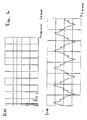
- FIG. 5 to 7 show current and voltage diagrams of an actually implemented circuit arrangement according to FIG. 2.
- FIG. 5 is an ozillogram for mains voltage and mains current of the circuit according to FIG. 2.
- the current curve I shows an approximately sinusoidal curve of the mains current. Without that Harmonic filter in the circuit of Fig. 2 results in a current during 1/10 to 1/15 of the half wave. Such a current spike would lead to grid repercussions, which have to be limited due to legal regulations. Due to the harmonic filter, the maximum of the current is reduced and the current is distributed over the entire half-wave, so that the desired approximation to a sinusoidal current curve results.
- FIG. 6 shows the harmonic analysis of the mains current shown in FIG. 5.
- the harmonic component of the mains current is far below the limit values permitted by VDE / IEC.
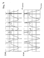
- FIG. 7 shows lamp current and lamp voltage of a circuit arrangement according to FIG. 2.
- the curves of lamp current I and lamp voltage U each show a peak superimposed on a sine curve on the positive half-wave. This peak corresponds to the turn-on time of transistor T1.
- the low-pressure discharge lamp can be operated with such a current or voltage without disadvantageous side effects or a shorter service life.
- FIG. 8 shows the basic structure of a further circuit arrangement for the high-frequency operation of a low-pressure discharge lamp LL1.
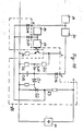
- Reference numerals a - j in FIG. 8 are also used in FIGS. 9-11 to show the connection points of the various circuit blocks in FIG. 8.
- the circuit arrangement includes a high-frequency filter 10, a mains rectifier 12, an active harmonic filter 13, a smoothing capacitor 14, a single-ended high-frequency lamp generator 15, control electronics 16, a driver circuit 17, an overvoltage monitor 18, a starting circuit 19 and an electronics supply 20.
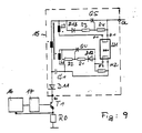
- FIG. 9 shows the circuit diagram of the circuit arrangement of the two additional secondary heating windings L3 and L4, which are connected to the heating coils E2, H2 and E1, H1 with the thyristors Q4 and Q5.
- the connection depends on the operating state of the lamp.
- a lamp which has not yet been ignited or is in the starting process shows an increased operating and ignition voltage, which is also available as a secondary voltage in the form of a winding on the windings L3 and L4 and is used as a trigger voltage.
- the ignition point for the thyristors Q4 and Q5 is derived via the voltage divider R1 / R2 and R3 / R4.
- the trigger voltage is no longer reached, so that the heating remains switched off. If the operating voltage of the lamp increases, e.g. B. at low operating temperatures or with a dimmed lamp, the trigger voltage is reached, whereby the heating of the filaments automatically switches on. If the heating coils fail due to an interruption, the diodes D12 and D13 prevent an impermissibly high current load on the voltage divider resistors.
- the starting behavior can be further improved by increasing the switching frequency of the single-cycle high-frequency lamp generator, because each switching cycle delivers a heating current pulse.
- the frequency increase is realized depending on the first time the electronics supply voltage is applied to the control electronics.
- FIG. 9 also shows the overcurrent detection of the emitter current from T1 via the voltage drop across the resistor RO, which is connected in series with the emitter. If a certain current limit value is reached, the corresponding voltage drop acts on the control electronics 16 in such a way that the driver circuit 17 is switched off and thus the switching transistor T1 is switched off. This circuit arrangement thus acts as an electronic overcurrent protection.
- the collector voltage of the switching transistor is switched to the trigger diode Q1 via the voltage divider R5 / R6 and the diode D15.
- the trigger diode Q1 can also be switched via the diode D16 depending on the level of the electronics supply voltage.
- the capacitor C13 prevents the trigger circuit from responding to voltage spikes that only occur for a short time and, when the trigger diode is switched through, provides the required ignition current for the thyristor Q2. If the thyristor Q2 is ignited by means of a trigger pulse, it drops into a latched state via the resistor R7.
- FIG. 11 shows the circuit section of the circuit arrangement for the starting circuit 19 and for the electronic self-supply 20.
- the capacitor C14 is charged via the resistor R10 and the diode D10.
- a maximum permissible voltage value at C14 is specified via the voltage divider R8 / R9, at which the thyristor Q3 connects this voltage to the electronics supply.
Landscapes
- Circuit Arrangements For Discharge Lamps (AREA)
- Power Conversion In General (AREA)
- Dc-Dc Converters (AREA)
- Burglar Alarm Systems (AREA)
- Slot Machines And Peripheral Devices (AREA)
- Design And Manufacture Of Integrated Circuits (AREA)
Applications Claiming Priority (2)
| Application Number | Priority Date | Filing Date | Title |
|---|---|---|---|
| EP89104702 | 1989-03-16 | ||
| EP89104702 | 1989-03-16 |
Publications (3)
| Publication Number | Publication Date |
|---|---|
| EP0389847A2 true EP0389847A2 (fr) | 1990-10-03 |
| EP0389847A3 EP0389847A3 (fr) | 1992-03-04 |
| EP0389847B1 EP0389847B1 (fr) | 1995-02-15 |
Family
ID=8201092
Family Applications (1)
| Application Number | Title | Priority Date | Filing Date |
|---|---|---|---|
| EP90104513A Expired - Lifetime EP0389847B1 (fr) | 1989-03-16 | 1990-03-09 | Circuit |
Country Status (10)
| Country | Link |
|---|---|
| US (1) | US5070276A (fr) |
| EP (1) | EP0389847B1 (fr) |
| JP (1) | JPH03173347A (fr) |
| KR (1) | KR900015582A (fr) |
| CN (1) | CN1024979C (fr) |
| AT (1) | ATE118666T1 (fr) |
| CA (1) | CA2012441A1 (fr) |
| DE (1) | DE59008453D1 (fr) |
| ES (1) | ES2068266T3 (fr) |
| IN (1) | IN171097B (fr) |
Cited By (3)
| Publication number | Priority date | Publication date | Assignee | Title |
|---|---|---|---|---|
| DE4217822A1 (de) * | 1991-10-18 | 1993-04-22 | Heinrich Korte | Elektronisches vorschaltgeraet |
| WO1995035645A1 (fr) * | 1994-06-22 | 1995-12-28 | Philips Electronics N.V. | Procede et agencement de circuit pour l'exploitation d'une lampe a decharge a haute pression |
| EP0714225A1 (fr) | 1994-11-22 | 1996-05-29 | Oy Helvar | Filtre pour un ballast électronique de lampe à décharge |
Families Citing this family (6)
| Publication number | Priority date | Publication date | Assignee | Title |
|---|---|---|---|---|
| US5682086A (en) * | 1995-10-05 | 1997-10-28 | Yin Nan Enterprises Co., Ltd. | Dynamic filter for an electronic ballast with a parallel-load resonant inverter |
| US6137234A (en) * | 1999-10-18 | 2000-10-24 | U.S. Philips Corporation | Circuit arrangement |
| US6396220B1 (en) * | 2001-05-07 | 2002-05-28 | Koninklijke Philips Electronics N.V. | Lamp ignition with compensation for parasitic loading capacitance |
| US7954961B2 (en) * | 2005-06-30 | 2011-06-07 | Koninklijke Philips Electronics N.V. | Method for driving a high-pressure gas discharge lamp of a projector system |
| EP2523305B1 (fr) * | 2011-05-12 | 2017-10-18 | Moog Unna GmbH | Dispositif d'alimentation d'urgence en énergie et procédé d'alimentation d'urgence en énergie |
| CN111243825B (zh) * | 2018-11-29 | 2023-06-16 | 阿尔贝特·莫伊雷尔 | 用于使铁磁材料消磁的装置 |
Family Cites Families (10)
| Publication number | Priority date | Publication date | Assignee | Title |
|---|---|---|---|---|
| DE3266600D1 (en) * | 1981-02-21 | 1985-11-07 | Emi Plc Thorn | Lamp driver circuits |
| JPS59128128A (ja) * | 1983-01-13 | 1984-07-24 | Matsushita Electric Works Ltd | 積載方法 |
| DE3303374A1 (de) * | 1983-02-02 | 1984-08-02 | Rheintechnik Weiland & Kaspar Kg, 6680 Neunkirchen | Stromversorgungsschaltung fuer leuchtstoffroehren |
| DE3312572A1 (de) * | 1983-04-08 | 1984-10-18 | Trilux-Lenze Gmbh + Co Kg, 5760 Arnsberg | Elektronisches vorschaltgeraet fuer eine leuchtstofflampe |
| SE444496B (sv) * | 1984-08-02 | 1986-04-14 | Innocap Ab | Kopplingsanordning for drivning av gasurladdningsror |
| US4873471A (en) * | 1986-03-28 | 1989-10-10 | Thomas Industries Inc. | High frequency ballast for gaseous discharge lamps |
| DE3611611A1 (de) * | 1986-04-07 | 1987-10-08 | Patent Treuhand Ges Fuer Elektrische Gluehlampen Mbh | Schaltungsanordnung zum hochfrequenten betrieb einer niederdruckentladungslampe |
| DE3623749A1 (de) * | 1986-07-14 | 1988-01-21 | Patent Treuhand Ges Fuer Elektrische Gluehlampen Mbh | Schaltungsanordnung zum betrieb von niederdruckentladungslampen |
| DE3700421A1 (de) * | 1987-01-08 | 1988-07-21 | Patent Treuhand Ges Fuer Elektrische Gluehlampen Mbh | Schaltungsanordnung zum betrieb einer niederdruckentladungslampe |
| US4904903A (en) * | 1988-04-05 | 1990-02-27 | Innovative Controls, Inc. | Ballast for high intensity discharge lamps |
-
1989
- 1989-05-24 IN IN400/CAL/89A patent/IN171097B/en unknown
-
1990
- 1990-03-09 DE DE59008453T patent/DE59008453D1/de not_active Expired - Fee Related
- 1990-03-09 AT AT90104513T patent/ATE118666T1/de not_active IP Right Cessation
- 1990-03-09 EP EP90104513A patent/EP0389847B1/fr not_active Expired - Lifetime
- 1990-03-09 ES ES90104513T patent/ES2068266T3/es not_active Expired - Lifetime
- 1990-03-13 US US07/492,457 patent/US5070276A/en not_active Expired - Fee Related
- 1990-03-16 JP JP2064478A patent/JPH03173347A/ja active Pending
- 1990-03-16 CN CN90101493A patent/CN1024979C/zh not_active Expired - Fee Related
- 1990-03-16 CA CA002012441A patent/CA2012441A1/fr not_active Abandoned
- 1990-03-16 KR KR1019900003678A patent/KR900015582A/ko not_active Withdrawn
Cited By (4)
| Publication number | Priority date | Publication date | Assignee | Title |
|---|---|---|---|---|
| DE4217822A1 (de) * | 1991-10-18 | 1993-04-22 | Heinrich Korte | Elektronisches vorschaltgeraet |
| WO1995035645A1 (fr) * | 1994-06-22 | 1995-12-28 | Philips Electronics N.V. | Procede et agencement de circuit pour l'exploitation d'une lampe a decharge a haute pression |
| US5608294A (en) * | 1994-06-22 | 1997-03-04 | U.S. Philips Corporation | High pressure lamp operating circuit with suppression of lamp flicker |
| EP0714225A1 (fr) | 1994-11-22 | 1996-05-29 | Oy Helvar | Filtre pour un ballast électronique de lampe à décharge |
Also Published As
| Publication number | Publication date |
|---|---|
| CN1024979C (zh) | 1994-06-08 |
| ATE118666T1 (de) | 1995-03-15 |
| EP0389847A3 (fr) | 1992-03-04 |
| CN1045677A (zh) | 1990-09-26 |
| IN171097B (fr) | 1992-07-18 |
| JPH03173347A (ja) | 1991-07-26 |
| DE59008453D1 (de) | 1995-03-23 |
| KR900015582A (ko) | 1990-10-27 |
| US5070276A (en) | 1991-12-03 |
| EP0389847B1 (fr) | 1995-02-15 |
| CA2012441A1 (fr) | 1990-09-16 |
| ES2068266T3 (es) | 1995-04-16 |
Similar Documents
| Publication | Publication Date | Title |
|---|---|---|
| DE3587792T2 (de) | Elektronisches Vorschaltgerät für Leuchtstofflampen. | |
| DE4002334C2 (de) | Schaltung zum Betreiben einer elektrischen Entladelampe in einem Kraftfahrzeug | |
| DE60006046T2 (de) | Vorschaltgerät für Starkstromgasentladungslampe | |
| DE102004025597B4 (de) | Verfahren und Schaltung zur Leistungsfaktorkorrektur (PFC) | |
| EP0256231A2 (fr) | Circuit de commande pour une alimentation à découpage à courant d'entrée de forme sinusoidale pour transformer une tension alternative de forme sinusoidale en tension continue régulée | |
| EP0781077A2 (fr) | Circuit pour alimenter une lampe | |
| DE3246454A1 (de) | Wechselrichter mit einem einen reihenresonanzkreis und eine entladungslampe enthaltenden lastkreis | |
| DE2705968A1 (de) | Starter- und vorschaltanordnung fuer gasentladungslampe | |
| EP0522266A1 (fr) | Ballast protégé contre surtension | |
| DE2827693A1 (de) | Wechselrichter und dessen verwendung in einem batterieladegeraet | |
| EP0439240B1 (fr) | Ballast électronique | |
| DE19843643B4 (de) | Schaltungsanordnung zum Starten und Betreiben einer Hochdruck-Entladungslampe | |
| DE2948287A1 (de) | Schaltungsanordnung fuer hochintensitaetsentladungslampen | |
| DE3303374A1 (de) | Stromversorgungsschaltung fuer leuchtstoffroehren | |
| EP0389847B1 (fr) | Circuit | |
| DE3014419C2 (de) | Vorschaltgerät für eine Entladungslampe | |
| EP0057910B1 (fr) | Circuit pour l'alimentation régulée d'un utilisateur | |
| EP0331157B1 (fr) | Alimentation de puissance à découpage | |
| DE2445033B2 (de) | Gleichstromumrichter | |
| DE2445032C2 (de) | Schaltungsanordnung zur Erzeugung einer Einschaltspannung für den Steuerteil eines Mittelfrequenz-Umrichters | |
| EP1326484A2 (fr) | Appareil pour alimenter des lampes à décharge | |
| DE3530638A1 (de) | Schaltungsanordnung zum starten und betrieb von gasentladungslampen | |
| EP0635171B1 (fr) | Bloc electronique d'alimentation a decoupage | |
| EP1472776B1 (fr) | Dispositif de commutation pour corriger le facteur de puissance | |
| DE4036604A1 (de) | Schaltungsanordnung zum betrieb einer entladungslampe |
Legal Events
| Date | Code | Title | Description |
|---|---|---|---|
| PUAI | Public reference made under article 153(3) epc to a published international application that has entered the european phase |
Free format text: ORIGINAL CODE: 0009012 |
|
| AK | Designated contracting states |
Kind code of ref document: A2 Designated state(s): AT BE CH DE DK ES FR GB GR IT LI LU NL SE |
|
| PUAL | Search report despatched |
Free format text: ORIGINAL CODE: 0009013 |
|
| AK | Designated contracting states |
Kind code of ref document: A3 Designated state(s): AT BE CH DE DK ES FR GB GR IT LI LU NL SE |
|
| 17P | Request for examination filed |
Effective date: 19920826 |
|
| 17Q | First examination report despatched |
Effective date: 19940121 |
|
| GRAA | (expected) grant |
Free format text: ORIGINAL CODE: 0009210 |
|
| AK | Designated contracting states |
Kind code of ref document: B1 Designated state(s): AT BE CH DE DK ES FR GB GR IT LI LU NL SE |
|
| PG25 | Lapsed in a contracting state [announced via postgrant information from national office to epo] |
Ref country code: NL Effective date: 19950215 Ref country code: GR Free format text: LAPSE BECAUSE OF FAILURE TO SUBMIT A TRANSLATION OF THE DESCRIPTION OR TO PAY THE FEE WITHIN THE PRESCRIBED TIME-LIMIT Effective date: 19950215 Ref country code: DK Effective date: 19950215 Ref country code: BE Effective date: 19950215 |
|
| REF | Corresponds to: |
Ref document number: 118666 Country of ref document: AT Date of ref document: 19950315 Kind code of ref document: T |
|
| PG25 | Lapsed in a contracting state [announced via postgrant information from national office to epo] |
Ref country code: AT Effective date: 19950309 |
|
| ET | Fr: translation filed | ||
| GBT | Gb: translation of ep patent filed (gb section 77(6)(a)/1977) |
Effective date: 19950221 |
|
| REF | Corresponds to: |
Ref document number: 59008453 Country of ref document: DE Date of ref document: 19950323 |
|
| PG25 | Lapsed in a contracting state [announced via postgrant information from national office to epo] |
Ref country code: LU Free format text: LAPSE BECAUSE OF NON-PAYMENT OF DUE FEES Effective date: 19950331 Ref country code: LI Effective date: 19950331 Ref country code: CH Effective date: 19950331 |
|
| REG | Reference to a national code |
Ref country code: ES Ref legal event code: FG2A Ref document number: 2068266 Country of ref document: ES Kind code of ref document: T3 |
|
| ITF | It: translation for a ep patent filed | ||
| PG25 | Lapsed in a contracting state [announced via postgrant information from national office to epo] |
Ref country code: SE Effective date: 19950515 |
|
| NLV1 | Nl: lapsed or annulled due to failure to fulfill the requirements of art. 29p and 29m of the patents act | ||
| REG | Reference to a national code |
Ref country code: CH Ref legal event code: PL |
|
| PLBE | No opposition filed within time limit |
Free format text: ORIGINAL CODE: 0009261 |
|
| STAA | Information on the status of an ep patent application or granted ep patent |
Free format text: STATUS: NO OPPOSITION FILED WITHIN TIME LIMIT |
|
| 26N | No opposition filed | ||
| PGFP | Annual fee paid to national office [announced via postgrant information from national office to epo] |
Ref country code: ES Payment date: 19970531 Year of fee payment: 8 |
|
| PGFP | Annual fee paid to national office [announced via postgrant information from national office to epo] |
Ref country code: GB Payment date: 19980302 Year of fee payment: 9 |
|
| PG25 | Lapsed in a contracting state [announced via postgrant information from national office to epo] |
Ref country code: ES Free format text: LAPSE BECAUSE OF THE APPLICANT RENOUNCES Effective date: 19980310 |
|
| PGFP | Annual fee paid to national office [announced via postgrant information from national office to epo] |
Ref country code: FR Payment date: 19980317 Year of fee payment: 9 |
|
| PG25 | Lapsed in a contracting state [announced via postgrant information from national office to epo] |
Ref country code: GB Free format text: LAPSE BECAUSE OF NON-PAYMENT OF DUE FEES Effective date: 19990309 |
|
| GBPC | Gb: european patent ceased through non-payment of renewal fee |
Effective date: 19990309 |
|
| PG25 | Lapsed in a contracting state [announced via postgrant information from national office to epo] |
Ref country code: FR Free format text: LAPSE BECAUSE OF NON-PAYMENT OF DUE FEES Effective date: 19991130 |
|
| REG | Reference to a national code |
Ref country code: FR Ref legal event code: ST |
|
| PGFP | Annual fee paid to national office [announced via postgrant information from national office to epo] |
Ref country code: DE Payment date: 20000526 Year of fee payment: 11 |
|
| REG | Reference to a national code |
Ref country code: ES Ref legal event code: FD2A Effective date: 20001009 |
|
| PG25 | Lapsed in a contracting state [announced via postgrant information from national office to epo] |
Ref country code: DE Free format text: LAPSE BECAUSE OF NON-PAYMENT OF DUE FEES Effective date: 20020101 |
|
| PG25 | Lapsed in a contracting state [announced via postgrant information from national office to epo] |
Ref country code: IT Free format text: LAPSE BECAUSE OF NON-PAYMENT OF DUE FEES;WARNING: LAPSES OF ITALIAN PATENTS WITH EFFECTIVE DATE BEFORE 2007 MAY HAVE OCCURRED AT ANY TIME BEFORE 2007. THE CORRECT EFFECTIVE DATE MAY BE DIFFERENT FROM THE ONE RECORDED. Effective date: 20050309 |