EP0390692A2 - Verfahren und Vorrichtung zur Herstellung einer Dünnschicht und Sensor - Google Patents
Verfahren und Vorrichtung zur Herstellung einer Dünnschicht und Sensor Download PDFInfo
- Publication number
- EP0390692A2 EP0390692A2 EP90400864A EP90400864A EP0390692A2 EP 0390692 A2 EP0390692 A2 EP 0390692A2 EP 90400864 A EP90400864 A EP 90400864A EP 90400864 A EP90400864 A EP 90400864A EP 0390692 A2 EP0390692 A2 EP 0390692A2
- Authority
- EP
- European Patent Office
- Prior art keywords
- substrate
- film
- target
- enzyme
- isfet
- Prior art date
- Legal status (The legal status is an assumption and is not a legal conclusion. Google has not performed a legal analysis and makes no representation as to the accuracy of the status listed.)
- Withdrawn
Links
Images


Classifications
-
- C—CHEMISTRY; METALLURGY
- C23—COATING METALLIC MATERIAL; COATING MATERIAL WITH METALLIC MATERIAL; CHEMICAL SURFACE TREATMENT; DIFFUSION TREATMENT OF METALLIC MATERIAL; COATING BY VACUUM EVAPORATION, BY SPUTTERING, BY ION IMPLANTATION OR BY CHEMICAL VAPOUR DEPOSITION, IN GENERAL; INHIBITING CORROSION OF METALLIC MATERIAL OR INCRUSTATION IN GENERAL
- C23C—COATING METALLIC MATERIAL; COATING MATERIAL WITH METALLIC MATERIAL; SURFACE TREATMENT OF METALLIC MATERIAL BY DIFFUSION INTO THE SURFACE, BY CHEMICAL CONVERSION OR SUBSTITUTION; COATING BY VACUUM EVAPORATION, BY SPUTTERING, BY ION IMPLANTATION OR BY CHEMICAL VAPOUR DEPOSITION, IN GENERAL
- C23C14/00—Coating by vacuum evaporation, by sputtering or by ion implantation of the coating forming material
- C23C14/22—Coating by vacuum evaporation, by sputtering or by ion implantation of the coating forming material characterised by the process of coating
- C23C14/34—Sputtering
- C23C14/46—Sputtering by ion beam produced by an external ion source
-
- C—CHEMISTRY; METALLURGY
- C23—COATING METALLIC MATERIAL; COATING MATERIAL WITH METALLIC MATERIAL; CHEMICAL SURFACE TREATMENT; DIFFUSION TREATMENT OF METALLIC MATERIAL; COATING BY VACUUM EVAPORATION, BY SPUTTERING, BY ION IMPLANTATION OR BY CHEMICAL VAPOUR DEPOSITION, IN GENERAL; INHIBITING CORROSION OF METALLIC MATERIAL OR INCRUSTATION IN GENERAL
- C23C—COATING METALLIC MATERIAL; COATING MATERIAL WITH METALLIC MATERIAL; SURFACE TREATMENT OF METALLIC MATERIAL BY DIFFUSION INTO THE SURFACE, BY CHEMICAL CONVERSION OR SUBSTITUTION; COATING BY VACUUM EVAPORATION, BY SPUTTERING, BY ION IMPLANTATION OR BY CHEMICAL VAPOUR DEPOSITION, IN GENERAL
- C23C14/00—Coating by vacuum evaporation, by sputtering or by ion implantation of the coating forming material
- C23C14/06—Coating by vacuum evaporation, by sputtering or by ion implantation of the coating forming material characterised by the coating material
- C23C14/12—Organic material
-
- G—PHYSICS
- G01—MEASURING; TESTING
- G01N—INVESTIGATING OR ANALYSING MATERIALS BY DETERMINING THEIR CHEMICAL OR PHYSICAL PROPERTIES
- G01N27/00—Investigating or analysing materials by the use of electric, electrochemical, or magnetic means
- G01N27/26—Investigating or analysing materials by the use of electric, electrochemical, or magnetic means by investigating electrochemical variables; by using electrolysis or electrophoresis
- G01N27/403—Cells and electrode assemblies
- G01N27/414—Ion-sensitive or chemical field-effect transistors, i.e. ISFETS or CHEMFETS
- G01N27/4145—Ion-sensitive or chemical field-effect transistors, i.e. ISFETS or CHEMFETS specially adapted for biomolecules, e.g. gate electrode with immobilised receptors
Definitions
- This invention relates to a method of forming on a substrate a thin film such as a functional film used as a reference electrode of an ion sensor, and apparatus for forming a thin film suitable for carrying out the method and a biosensor and chemical sensor such as an ISFET (ion sensitive field effect transistor) sensor having a thin film formed by the apparatus.
- a thin film such as a functional film used as a reference electrode of an ion sensor
- apparatus for forming a thin film suitable for carrying out the method and a biosensor and chemical sensor such as an ISFET (ion sensitive field effect transistor) sensor having a thin film formed by the apparatus.
- ISFET ion sensitive field effect transistor
- Ion sensors or the like generally use reference electrodes for reference potential generation.
- this reference electrde there are many attempts of manufacturing hydrophobic organic thin films consisting of hydrophobic fluororesins, particularly polytetrafluoroethylene (available under a trademark "Teflon”) by a dry process such as a deposition process or a spattering process.
- Teflon polytetrafluoroethylene
- CVD chemical vapor deposition
- organic thin films can find extensive applications to passivation films and seal materials because it is possible to obtain films which are rich in machining property and chemically stable.
- LB Liuir Blodgett
- electrolytic process As method of forming thin film in a wet state, there are a LB (Langmuir Blodgett) process and an electrolytic process. In these processes, thin films can be formed at room temperature. However, substances which can be used for film formation are limited, and thus it is possible to obtain perfect insulating film.
- ion sensors utilizing MOSFETs capable of fine machining using semiconductor manufacture technology i.e., ISFET sensors
- ISFET sensors have been developed as solid-state very small sensors, with reported sizes less than 10 microns.
- reference electrodes with polystyrene thin film and hydrophobic organic polymer film on gate insulating film are disclosed in Japanese Patent Disclosures 58-103658 and 58-34352.
- enzyme sensors for measuring the substrate concentration using enzyme electrodes by an amperometric process, and particularly enzyme sensors for directly measuring enzymic reaction from oxidization/reduction reaction of electron movement media (mediators) are well known.
- enzyme sensors are mainly used for clinical chemical analysis, and those for glucose, urea and neutral and phosphoric fat as subject of measurement are in practical use.
- an enzymic reaction in case of ⁇ -D-glucose (grape sugar) as subject of measurement is expressed as
- ⁇ -D-glucose consumes O2 with an action of ⁇ -D-glucose (GOX) to generate organic acid (gluconolactone) and hydrogen peroxide (H2O2). Therefore, glucose concentration can be measured from the amount of generated hydrogen peroxide and gluconolactone or amount of consumed oxygen.
- GOX ⁇ -D-glucose
- H2O2 hydrogen peroxide
- a method for measuring the glucose concentration according to the amount of generated hydrogen peroxide a method is adopted, in which the generated hydrogen peroxide is oxidized with metal electrode, and the oxidizing current is measured. Alternatively, the generated hydrogen peroxide is reduced, and the reducing current is measured.
- these oxidizing and reducing currents are subject to the influence of oxygen.
- prior art detection electrode is liable to be influenced by changes in the surface state.
- the principle of measurement by electrochemical means adopts a sensor sutructure, which comprises electrode substrate, liquid, enzymefixed film and liquid under test. Therefore, miniaturization of sensor is difficult due to liquid present between electrode and film.
- An object of the invention is to provide a method of manufacturing substrate with a thin film such as a satisfactorily hydrophobic film, which is excellent in reproducibility with respect to the film composition of the thin film and orientation thereof and never causes thermal damage.
- a method of manufacturing a substrate with a hydrophobic film which comprises a step of installing target consisting essentially of a hydrophobic compound at a predetermined position in a reaction chamber and a step of ionizing rare gas introduced into the reaction chamber, ionizing rare gas, accelerating ions in an acceleration voltage range of 0.1 to 100 kV while converting the ions into neutral atoms, and irradiating the target with the neutral atom beam for spattering, thereby causing growth of a hydrophobic compound on a predetermined substrate surface to manufacture a substrate with a hydrophobic film.
- rare gas or argon (Ar) with a high spattering factor is introduced into a reaction chamber in vacuum (or the order of 3 x 10 ⁇ 5 Torr) and ionized with a cold cathode, the ions are accelerated in a high voltage electric field and then passed through an electronic atmosphere for neutralization, and the target is irradiated with high speed neutral particles (i.e., neutral atom beam), thus forming a thin film on an intended substrate by utilizing the spattering phenomenon.
- the spattering process unlike the vacuum deposition process or ion injection process utilizing the movement of energy, kinetic energy of rare gas is directly converted into kinetic energy of atoms or molecules of the target. A dense thin film thus can be formed even with high-melting materials or alloys.
- the neutral beam is substantially free from ions (usually containing 1 % or less of ions).
- a beam containing ions is unsuitable because with an insulating or organic substance ions may cause charge-up, discharge or decomposition.
- the spattering process using a neutral atom beam is substantially free from ion particles. Therefore, the formation and composition of pin holes at the time of thin film formation are subject to less changes, and superior reproducibility of thin film can be obtained.
- the present invention is predicated in a finding that by using the neutral atom beam spattering process in forming a hydrophobic film of a fluorine compound or the like and controlling the beam irradiation condition, particularly accelerated voltage, it is possible to increase the content of fluorine (F) in C-F bond coupling. Thus, it is possible to approach the F/C ratio as designed. Also, heat storage on the target can be prevented by turning the target.
- the accelerating voltage is suitable in a range of 0.1 to 100 kV, preferably in a range of 1 to 10 kV. Where the voltage is below 0.1 kV, sufficient spattering can not be obtained with a neutral atom beam of rare gas such as argon (Ar). Where the voltage is higher than 100 kV, neutralized argon or the like is injected into the target, thus reducing the efficiency of spattering.
- a desired acceleration voltage can be selected in relation to the spattering time. Particularly, it is suitable to set the spattering time to 60 minutes and accelerating voltage to 8 kV. Further, for increasing the spattering efficiency, the angle between the neutral atom beam and target surface is suitable 15 to 60°C.
- the substrate is suitably disposed on a normal to the target surface at a point thereof bombarded by the neutral atom beam. Further, it is desired to effect parallel movement of the substrate repeatedly to obtain a homogenious thin film.
- the degree of vaccum at the time of spattering is suitably 10 ⁇ 4 Torr or less. Further, the temperature is suitably in a range of -20 to 60°C. Further, to prevent temperature rise due to irradiation of target with beam and thus prevent resultant decomposition, the target is desirably cooled down by rotating it.
- hydrophobic compound may be selected polytetrafluoroethylene, ethylene tetrafluoride-perfluoroalkylvinylether copolymer, ethylene tetrafluoro-propyrene hexafluoride copolymer, ethylene tetrafluoride-ethylene copolymer, ethylene trifluoride-ethylene copolymer, ethylene trifluorochloride polymer and vinylidene fluoride polymer.
- polyolefin resins such as polypropyrene and polyethylene, polystyrene, polyimide, polycarbonate and hydrophobic resins having functional groups.
- Another object of the invention is to provide an apparatus for manufacturing thin film, which permits formation not only of thin films of inorganic substances and multi-layer bodies, laminations and mixtures of thin films of inorganic substances but also of perfect insulating films.
- an apparatus for manufacturing thin film by accumulating spattered particles on a predetermined substrate surface which comprises a vacuum chamber, a target base provided in the vacuum chamber and for holding a support, neutral beam generation means for irradiating the target supported on the target base with a neutral beam, a substrate base for supporting the substrate and shutter means provided between the substrate base and target base for controlling the passage and blocking of spattered particles.
- a plurality of spattering means each including neutral beam generation means, a target base and shutter means are provided such that spattered particles generated by the individual spattering means are collected on the substrate base, or a plurality of neutral beam generation means are provided such that the target is irradiated by neutral beams emitted from the individual neutral beam generation means, thus improving the uniformity of the film thickness distribution.
- a substrate base drive mechanism capable of causing rotation, liner motion and arcular motion of and/or scanning the substrate base is provided for obtaining a uniform film thickness in a predetermined substrate surface, and the substrate base is provided with substrate temperature control means.
- the apparatus for manufacturing a thin film suitably comprises a first front chamber provided adjacent to the vacuum chamber, first on-off means for on-off controlling the communication between the front chamber and vacuum chamber, a first moving mechanism for moving the target between the vacuum chamber and first front chamber, a second front chamber provided adjacent to the vacuum chamber, second on-off means for on-off controlling the communication between the second front chamber and vacuum chamber and a second moving mechanism for moving the substrate base between the vacuum chamber and second front chamber.
- it suitably comprises on-off means for on-off controlling the communication between the neutral beam generation means and vacuum chamber.
- a further object of the invention is to provide a minute ISFET sensor integrally comprising a solid-state reference FET having stable characteristics and an ISFET and a method of manufacturing the same.
- ISFET sensor which comprises a reference FET including a gate section and a solid film formed on the gate section and having an electrically conductive layer, a halogenated silver layer, a hydrohobic resin layer and a halide layer and generating a reference potential and an ISFET electrically isolated from the reference FET and generating an output potential or current corresponding to the concentration of ions under measurement, the concentration of ions under measurement being measured according to the output potentials or currents of the reference FET and ISFET.
- the reference FET and ISFET are suitably formed on the same substrate. Further, it is suitable that the halide layer in the solid film contains a halide salt and that portions of the reference FET and ISFET other than the gate sections are covered with an insulating film.
- the ISFET according to the invention is suitably used by being mounted on an end of a catheter, and it is suitable that a temperature measurement element is provided for temperature compensation of the output potential or current according to the output of the temperature measurement element.
- an ISFET sensor which comprises a step of manufacturing a plurality of FETs by forming source and drain regions in a semiconductor substrate and forming a gate insulating film on semiconductor substrate surface in a channel region between the source and drain regions, at least one of these FETs being used as a reference FET, the other FETs being used as ISFETs, a step of forming a conductive layer on the gate insulating film of the reference FET and a halogenated silver layer on the electrically conductive layer, and a step of forming solid film on the halogenated silver layer by successively forming a hydrophobic resin layer and halogen compound layer.
- a further object of the invention is to provide an enzyme sensor, which can measure substrate concentration of glucose or the like easily, in short period of time and accurately, is free from contamination and is capable of miniaturization, and a method of manufacturing the same.
- an enzyme sensor which comprises an electrically conductive substrate and a single molecule film covering at least part of the electrically conductive substrate and including an electron movement medium and enzyme.
- electron movement reaction i.e., oxidization/reduction reaction
- the enzyme reaction is caused to measure the enzyme reaction from changes in the electron movement reaction.
- the electron movement reaction is detected as changes in current at a constant active potential on the electron movement medium.
- the electron movement medium and enzyme are suitably fixed in the single molecule film in a directly bonded state to one another.
- the electron movement medium suitably consists of a compound having a redox center, which compound has a redox potential capable of oxidizing or reducing the active center having active center of enzyme.
- enzyme is glucose oxidase
- it is suitably ferrocene derivative, preferably ferrocene carbonate.
- compound having redox center may also be used quinone compounds triphosphopyridinenucleotide compounds and flavin adenine dinucleotide compounds.
- LB Liur Blodgett
- individual molecules are uniformly orientated on the electrically conductive substrate, and it is possible to readily form a thin film having a thickness corresonding to the length of the single molecule.
- reaction taking place on the film surface can be readily transferred onto an electrically conductive substrate. More particularly, it is possible to obtain a high sensitivity sensor.
- the thicknesses of the individualy layers of the LB film have hilgh order property, it is possible to form a stable lamination and readily control the film thickness and amount of enzyme in the film.
- an enzyme sensor which comprises a step of manufacturing an electrically conductive substrate, a step of forming single molecule film with uniform molecule orientation by developing a single molecule film substance on the surface of an enzyme solution containing an electron movement medium and applying a constant secondary external pressure and a step of forming a single molecule film containing electron movement medium and enzyme on the electrically conductive substrate by dipping the electrically conductive substrate in an enzyme solution with single molecule film formed on the surface.
- a fatty acid e.g., stearic acid (CH3(CH2)12COOH)
- stearic acid CH3(CH2)12COOH
- a single molecule film without satisfactory orientation is formed.
- oleic acid as piston oil
- a pressure is applied to the "Teflon” thin plate by the diffusion force of oleic acid, thus causing movement of the "Teflon” thin plate to one water surface until equilibrium between the opposite side pressures is attained.
- a secondary external pressure is applied to the single molecule film of stearic acid, thus improving the orientation.
- the electrically conductive substrate constitutes an electrode, and it may be manufactured by forming a metal film such as an iridium oxide (I r O x ) as electrode by means of spattering on the glass substrate or transparent conductive glass substrate (ITO:Indian Tin Oxide). However, it is possible to construct the entire substrate with a conductive material of metal or the like.
- a metal film such as an iridium oxide (I r O x ) as electrode by means of spattering on the glass substrate or transparent conductive glass substrate (ITO:Indian Tin Oxide).
- ITO Indian Tin Oxide
- the electrically conductive substrate may be formed on the gate section or extension of the gate section, thus permitting the miniaturization of the whole sensor including the output section.
- the hydrophobic film formed by the method according to the invention having the above features has very satisfactory reproduction of film composition, film orientation and polymerization. Thus, it is possible to efficiently form a hydrophobic film having excellent insulating property.
- the substrate having a thin film thus formed can be suitably used for a reference electrode and also for SAW (surface elastic wave device) and optical waveguide.
- SAW surface elastic wave device
- the neutral beam by generating a neutron beam after adjusting the beam irradiation position of the neutral beam generation means, the neutral beam bombards the target to cause the target material to be spattered out, and spattered particles are deposited on a substrate supported on the substrate base, thus forming a thin film.
- the spattered particles may contain impurities.
- a thin film without pinhole can be readily manufactured such that it has a thickness of 1,000 angstroms or below.
- chemical composition such as whether it is organic or inorganic.
- special performance films particularly effective for optical devices and opto-chemical devices such as insulating film of super-thin film and artificial grating (super-grating).
- insulating film of super-thin film and artificial grating super-grating
- a thin film as a lamination or a multi-layer body may be readily formed by using different materials for the individual targets and sequentially on-off operating the shutter means. Further, a mixture film may be formed by opening all the shutter means at a time.
- the uniformity of the film thickness distribution may be improved by providing a plurality of neutral beam generation means.
- the film thickness may be made uniform over a predetermined surface portion, particularly a step coverage can be improved when forming a thin film on a substrate having a step.
- the cover property of the film can be improved by providing the substrate base with heating means.
- the multi-layer film and lamination film may be readily formed.
- first or second front chamber in the vacuum chamber and also providing a mechanism for moving the substrate base or target base, it is possible to effect replacement of substrates or targets in a short period of time.
- on-off means between neutral beam generation means and vacuum chamber it is possible to readily perform maintenance and inspection of neutral beam generation means while holding vacuum in the vacuum chamber.
- each halogenated silver halide layer fulfills a function corresponding to that of the reference electrolyte and reference liquid chamber in a prior art reference electrode.
- the reference FET is formed as a solid FET by sequentilally forming an electrically conductive layer, a halide compound layer, a hodrophylic resin layer and a halide compound layer as respective solid films, miniaturization is readily possible.
- a constant potential can be readily obtained without being influenced by pH or the like, and the stability and durability can be improved.
- the reference FET and ISFET are formed integrally such that the concentration of ions under measurement can be measured on the basis of the output potentials or currents of the reference FET and ISFET, it is possible to manufacture the entire sensor as solid and miniaturized sensor. Further, by integrating the temperature measurement element it is possible to determine temperature-compensated ion concentration, thus improving the accuracy of measurement. Further, since an atom beam spattering device may be used for the formation of the solid film, it is possible to form film under a room temperature, high dimensional accuracy of pattern formation can be obtained, and mass production can be obtained by assembling the apparatus into a semiconductor manufacture process.
- the enzyme sensor having the above features according to the invention, electron movement medium and enzyme are fixed in the single molecule film, and therefore the following principle can be obtained.
- the enzyme used is glucose oxydase (GOX)
- GOX glucose oxydase
- FAD flavino-adenine dinucleotide
- enzyme can be indirectly oxidized and reduced. This phenomenon may be utilized for causing electron movement between enzyme and electrically conductive substrate (electrode) for directly electrochemically detecting enzymic reaction.
- Fig. 24 shows the status of electron movement due to the above reaction. More particularly, with such electron movement current in the electrically conductive substrate (electrode) is increased, and the glucose concentration can be measured from this current increase.
- the LB process is used for the formation of the enzyme-fixed film, it is possible to form film even if the electrode substrate is very minute in size. Since no inner liquid chamber or the like is necessary, there is no such problem as contamination of liquid under measurement. Particularly, utility as sensor in the medical field can be extremely increased.
- Embodiments 1 to 4 of the invention concerning method of manufacturing a substrate with a hydrophobic film according to the invention will be described with reference to Figs. 1 to 5.
- a thin film with a thickness of 100 to 370 angstroms was formed on a glass substrate using a neutral atom beam spattering apparatus shown in Fig. 1. More particularly, target 5 of polytetrafluoroethylene on turn-table 4 was irradiated with neutral atom beam 3 of argon (Ar) shot from FAB (fast atom bombardment) gun 2 in vacuum (3 x 10 ⁇ 5 Torr) at normal temperature, thus spattering out polytetrafluoroethylene molecules to grow a thin film substrate 6 on the target irradiated with the beam at point P on normal to the turn-table.
- neutral atom beam spattering apparatus shown in Fig. 1. More particularly, target 5 of polytetrafluoroethylene on turn-table 4 was irradiated with neutral atom beam 3 of argon (Ar) shot from FAB (fast atom bombardment) gun 2 in vacuum (3 x 10 ⁇ 5 Torr) at normal temperature, thus spattering out polytetrafluoroethylene molecules to grow
- the spattering time was set to 60 minutes.
- the spattering rate was set to 100 to 370 angstroms, and target 5 was rotated with turn-table 4 to prevent heat concentration at this time.
- the acceleration voltage was linearly related to the spattering speed in a range of 5 to 8 kV.
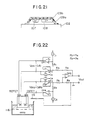
- Fig. 2 shows the results of analysis of the thin films formed with the individual voltages by ESCA (electron spectroscopy for chemical analysis).
- a polytetrafluoroethylene thin layer with a thickness of 150 angstroms was formed in the same way as in Embodiment 1 except for that a metal layer was formed on a glass substrate by a deposition process and then the acceleration voltage was set to 7 and 8 kV. On this layer a metal layer with a thickness of 2,000 angstroms was formed, thus forming an MIM element consisting of metal layer, polytetrafluoroethylene thin layer and metal layer.
- the insulating property of the MIM element in Embodiment 2 was examined, and it was satisfactory.
- the low frequency dielectric characteristics were measured by using an AC impedance process (a process of measuring a dry film with an AC process: manufactured by NF circuit, lock-in amp.).
- the dielectric constant i.e., 3.8 with film manufactured with 7 kV and 2.2 with film manufactured with 8 kV) over a wide frequency range of 50 Hz to 5 kHz.
- the dielectric strength was satisfactory, i.e., it was 4.7 kV/mm with film formed with 7 kV and 7 to 8 kV/mm with film formed with 8 kV.
- Spattering was carried out with the revolving rate of polytetrafluoroethylene target 5 set to 90 minutes/rotation and the neutral beam acceleration volatage of FAB 2 to 4, 5, 6, 7, 8 ,9 and 10 kV, thus forming each thin film with a thickness of about 260 angstroms on glass substrate 6.
- the ESCE peak of polytetrafluoroethylene of target 5 was as large as to correspond to CF3 or ( ⁇ CF2-CF2) ⁇ . It will be seen that with spattering effected with 8 kV it is possible to obtain bonding energy comparable to that in peak formation similar to polytetrafluoroethylene. Thus, it can be concluded that a film obtained with an acceleration voltage of 8 kV has substrantially the same composition as polytetrafluoroethylene. When the acceleration voltage is reduced from 7 to 4 kV, the peak intensity corresponding to ( ⁇ CF2-CF2) ⁇ is reduced, and the peak corresponding to coupling including ( ⁇ CF) ⁇ n turns to be increased. Therefore, it can be thought that a film with large CF is formed, which is deviated from the compoisition of polytetrafluoroethylene.
- argon (Ar) was used as rare gas, it is possible to use crypton (Kr) and xenon (Xe) heavier than argon as well.
- Fig. 6 is a schematic view showing the construction of an apparatus for manufacturing a thin film with a neutral atom beam as neutral beam as Embodiment 4 of the invention.
- reference numeral 10 designates a vacuum chamber.
- atom beam gun 11 for generating a neutral atom beam (manufactured by Ion Tec Co., Ltd.), target base 12 for supporting target 12a, substrate base 13 for supporting substrate 13a such as saphire substrate for thin film formation and shutter 14.
- Outside vacuum chamber 10 are disposed gas bonb 15, in which an inert gas such as argon gas (Ar), and gas flow controller 16, and argon gas is supplied at a predetermined rate through gas supply line 17 to atom beam gun 11.
- Outside vacuum chamber 10 is disposed high voltage source 18 for beam generation is disposed, with its positive terminal 18a connected to atom beam gun 11 through lead terminal 19 provided on a side wall of vacuum chamber 10.
- GND terminal 18b of high voltage source 18 is grounded by getting connected to a side wall of vacuum chamber 10.
- high voltage source 18 is used one with voltage range of 0 to 10 kV and maximum current of 10 mA.
- Atom beam gun 11 is supported on top of support post 21 through height adjustment system 20, with the lower end of support post 21 secured to the bottom of vacuum chamber 10.
- Height adjustment system 20 has knob 22, permitting adjustment of the setting angle of atom beam gun 11 to adjust the atom beam irradiation angle.
- the outer side of atom beam gun 11 is cooled by water-cooling pipe 23.
- Target base 12 and substrate supporting base 13 are disposed one above another and comprises respective turn-tables. They are driven by respective motor 24 and 25.
- Motor 25 is arcularly reciprocable by an arcular movement mechanism 26.
- Arcular movement machanism 26 compjrises arcular rail 26a and carrier 26b movable along rail 26a. On carrier 26b is mounted motor 25 for driving substrate supporting base 13.
- Shutter 14 is adapted to be disposed between target base 12 and substrate supporting base 13, and it opens and closes a passage, through which spattered particles pass, from external handle 31 through which spattered particles pass, from external handle 31 through turning rod 30.
- Vacuum chamber 10 is evacuated by rotary pump 32 and diffusion pump 33.
- vacuum chamber 10 evacuated to high vacuum (to be 10 ⁇ 5 Torr or below) with rotary pump 32 and diffusion pump 33, high voltage is applied from high voltage source 18 to atom beam gun 11, and argon gas is caused to flow through gas bomb and gas flow controller 16.
- gas atoms are ionized by the high voltage, and the ions thus generated are accelerated in an electric field.
- atom beam gun 11 ion charge is neutralized, thus generating a high speed neutral atom beam.
- This neutral atom beam bombards target 12a on target supporting base 12 and thus spatters the target material, and the spattered particles are attached to the opposed surface of substrate 13a.
- target 12a formed such that it comprises a plurality of divisions of different materials and with target base 12 rotated at a constant rate it is possible to obtain a thin film comprising a multi-layer body.
- the spattered particles contain impurities, and therefore it is suitable to dispose shutter 14 between target 12a and substrate 13a for opening and closing the pass of spattered particles. By so doing, formation of a thin film containing impurities can be prevented.
- the spattered particles come out with a cosine-curve distribution and thus has corresponding large thickness distribution.
- substrate supporting base 13 may be rotated, or carrier 26b or motor 28 may be operated.
- Atom beam gun 11 includes an ionizing chamber such as a cold cathode, an ion acceleration chamber and an ion neutralization mechanism. Therefore, the beam emitted from atom beam gun 11 is desirably perfectly neutralized, but several per cent (less than 5 %) may remain without being neutralized.
- a sheet of "Teflon" (a trademark) was provided as target material on target supporting base 12, sapphire substrate (20 mm by 20 mm by 0.5 mm) was mounted on substrate supporting base 13, and the angle between atom beam and horizontal surface of target was set to 30 to 45 degrees. The position of substrate base 13 was adjusted such that spattered particles are deposited on the sapphire substrate. Subsequently, vacuum chamber 10 is evacuated to be 2 x 10 ⁇ 6 Torr or below with rotary pump 32 and diffusion pump 33. Then, the rate of argon gas flow was set to 0.5 sccm/min., argon gas was supplied to atom beam gun 11, and voltage was increased slowly up to 8 kV to generate a neutral atom beam.
- Teflon a trademark
- Target base 12 was turned by one rotation for 30 minutes to prevent thermal decomposition of the target.
- Substrate supporting base 13 was rotated at a position deviated by 4 to 8 mm from a point right above the point, at which target 12a was irradiated by the neutral atom beam. Under this condition, spattering was carried out for one hour to obtain a thin film with a thickness of 200 to 500 angstroms.
- This thin film was analyzed with ESCA (Electron Spectroscopy for Chemical Analysis). As a result, peaks corresponding to F IS and C IS (C-F bonding energy) were obtained, indicating that the thin film had the same composition as "Teflon".
- the breakdown voltage and resistance of the Teflon thin film were measured to be 18 kV/mm or above and 1014 ⁇ .cm (volume resistance), respectively, indicating a highly insulating property.
- the dielectric constant was 2.1, close to a value corresponding to the character of Teflon.
- Embodiment 4 was used to carry out spattering for 4 hours with the distance D between substrate supporting base 13 and target set to 10 and 20 mm and with substrate supporting base 13 rotated at 1,000 rpm.
- Fig. 8 shows film thickness distribution corresponding to spattering for one hour in this case. Labeled a in the Figure corresponds to the case where D is 10 mm, and b to the case where D is 20 mm. In both cases, the voltage condition of atom beam gun 11 was set to 7 kV/mA.
- the angle of substrate 13a was set to be in a range of ⁇ 45 degrees by arcularly moving carrier 26b about the center of substrate 13a (i.e., point z in Fig. 6). Doing so permitted formation of a film on a step portion of substrate with a step, indicating extreme improvement of the step coverage.
- Target base 12 and substrate supporting base 13 shown in Embodiment 4 are by no means limitative, modifications as shown in Figs. 11 to 14 may be used as well. More specifically, any structure may be used so long as it is one, in which strip-like target 12a is wound on roller 40 (Fig. 11), one, in which rod-like target 12a is moved linearly with rollers 41 (Fig. 12), an X-Y stage, preferably XYZ stage 42 (Fig. 13), or a combination of X-Y stage 43a and turn-table 43b (Fig. 14).
- a planetary dome type turn-table may suitably be used.
- substrate supporting base 13 may be heated with a temperature control mechanism to improve the adhesion of the film.
- a temperature control mechanism substrate supporting base 13 may be directly heated with a plate heater or the like. Alternatively, it may be heated with radiant heat energy from an infrared lamp.
- the atom beam gun by using one, which can provide uni-dimensional and two-dimensional array beams in addition to a single beam, it is possible to form a thin film having a uniform thickness in a broader range.
- Fig. 9 is a schematic view showing the construction of an apparatus for manufacturing thin film as Embodiment 5 of the invention.
- a plurality of,i.e., two in this embodiment, spattering means assemblies each consisting essentially of atom beam gun 11, target base 12 and shutter 14 are provided in common vacuum chamber 10.
- Parts like those in Embodiment 4 are designated by like reference numerals with omission of their repeated description.
- a thin film consisting essentially of a limination body may be manufactured by using different materials for all targets 12a and sequentially on-off operating shutters 14. Further, a mixture film may be manufactured by opening all shutters 14. Further, a film having satisfactory film thickness jdistribution characteristics can be formed by effecting spattering at a time with the same material used for all targets 12a.
- a reference electrode was formed by using the apparatus of Embodiment 5.
- a Teflon plate and silver chloride (AgCl) were used for target 12a, and a lamination film with a thickness of 400 angstroms and consisting essentially of alternately laminated silver chloride and Teflon layers was formed on a thin layer of silver (Ag) formed on a sapphire substrate.
- Fig. 10 shows the construction of an apparatus for forming a thin film as Embodiment 6 according to the invention.
- front chambers 44 and 45 are formed in opposite sides of or above and below vacuum chamber 10, and valve shutters 46 and 47 are provided as on-off means between front chambers 44 and 45 and vacuum chamber 10.
- a moving mechanism (not shown) for vertically moving target base 12 and substrate supporting base 13 is provided to permit replacement of target 12a and substrate 13a in a short period of time.
- target 12a and substrate 13a are moved into front chambers 44 and 45, and then valve shutters 46 and 47 are closed. Subsequently, window 48 is opened, and then target 12a and substrate 13a are replaced. After replacement, window 37 is closed, then valve shutters 46 and 47 are opened, and target 12a and substrate 13a are brought back to the initial positions.
- target 12a and substrate 13a can be replaced in a short period of time while holding substantial vacuum in vacuum chamber 10.
- Atom beam gun 11 is mounted on each side wall of vacuum chamber 10, and a valve shutter 49 is provided between each atom beam gun 11 and vacuum chamber 10. Thus, each atom beam gun 11 can be taken out while holding vacuum in vacuum chamber 10.
- target 12a can be replaced in a short period of time.
- uniformity of the film thickness can be improved because the system is a multi-gun system.
- Fig. 15 is a perspective view showing the overall construction of ISFET sensor 100 as Embodiment 7 of the invention.
- reference FET 103 In this ISFET sensor 100, reference FET 103, ISFET 104 and temperature compensation diodes 105 and 106 are formed on the surface of SOS (silicon on sapphire) substrate 102 such that they are electrically insulated from one another.
- Reference FET 103 serves as reference electrode, and the concentration of ions under measurement is detected according to a differential output between output potential (reference potential) of reference FET 103 and output potential of ISFET 104.
- Fig. 16 shows sectional structure of reference FET 103.
- Source and drain regions 107 and 108 are formed by diffusion of n-type impurity, e.g., arsenic (As), in silicon layer 102a on SOS substrate 102.
- gate insulating film 109 consisting of silicon oxide (SiO2) film 109a and silicon nitride (Si3N4) film 109b.
- an electrically conductive layer consisting of chromium (Cr) layer 110a and silver (Ag) layer 110b.
- silver layer 110b is formed silver chloride (AgCl) layer 111 such as to cover the entire surface of silver layer 110b.
- lamination film 113 consisting essentially of alternate lamination of thin films of a hydrophobic resin, e.g., thin films 112a of polytetrafluoroethylene (PTFE), and silver chloride thin films 112b containing sodium chloride (NaCl).
- PTFE polytetrafluoroethylene
- NaCl sodium chloride
- Figs. 17 to 21 show sectional structures of various parts of the structure shown in Fig. 15.
- ISFET sensor 100 is manufactured in the following way. First, silicon layer 102a with a thickness of about 6,000 angstroms was patterned to an island form on SOS substrate 102 by wet etching using hydradine as etching liquid. Then, arsenic ions (As+) were selectively implanted in a concentration of 1 to 5 x 10¹⁵ atm/cm2 at 100 keV while forming PN junction 114 between diodes 105 and 106 by using an ion implantation unit (ULAVC, IXK-7000). Then, silicon oxide film 109a with a thickness of 1,000 angstroms was formed by thermal oxidization on gate sections of reference FET 103 and ISFET 104. Then, silicon nitride (Si3N4) film 109b with a thickness of 1,500 angstroms was formed by using a thermal CVD (chemical vapor deposition) process.
- Si3N4 silicon nitride
- contact holes were formed in correspondence to source and drain regions 107 and 108 and anodes and cathodes of diodes 105 and 106.
- electrode 115 consisting substantially of a chromium layer with a thickness of 500 angstroms and a copper layer with a thickness of 2 microns was formed in each of the contact holes. The contact holes were opened such that source region 107 of each FET was short-circuited to the substrate. Further, electrode was formed such that source electrode and anode electrode of diode were connected to each other.
- chromium layer 110a with a thickness of 50 to 200 angstroms was formed by the vacuum deposition process on gate insulating film 109 of reference FET 103 shown in Fig. 16 through a first metal mask.
- silver layer 110b with a thickness of 1,000 to 2,000 angstroms was deposition formed, and then the first metal mask is replaced with a slightly greater second mask, and silver chloride layer 111 with a thickness of 200 to 300 angstroms was formed such as to cover the entire surface of silver layer 110b.
- the mask was replaced with a further greater third mask, and spattering was carried out for one hour by using an argon atom beam spattering apparatus and with polytetrafluoroethylene (PTFE) as target under conditions of acceleration voltage of 8 kV and current of 1.0 mA to form polytetrafluoroethylene thin film 112a with a thickness of about 200 to 300 angstroms.
- PTFE polytetrafluoroethylene
- the mask was replaced with the second metal mask, and silver chloride layer 112b with a thickness of 200 to 300 angstroms and containing 1 to 100 mol% of sodium chloride (NaCl) was formed using a vacuum deposition process.
- polytetrafluoroethylene thin film 112a with a thickness of 200 to 300 angstroms was formed by spattering in the same way as described above.
- reference FET 103 was manufactured, which consists of lamination film 113 obtained by alternatively forming polytetrafluoroethylene thin films 112a and silver chloride layers 112b containing sodium chloride.
- contact electrodes were paste silver connected using leads constituted by a copper layer print pattern formed on a flexible substrate made of a polyimide material.
- ISFET 104 and reference FET 103 were covered except for gate sections with an insulating film consisting essentially of a polyimide resin and a silicone resin for electric insulation.
- ISFET sensor 100 As a driver for ISFET sensor 100 manufactured in the above way may be used one as shown in Fig. 22, including differential amplifiers OP1 to OP5, constant current sources I1 to I4 and resistors R1 to R6.
- This circuit is used as source follower to drive reference FET 103 and ISFET 104 as constant current sources I3 and I4 and constant voltage sources V DS1 and V DS2 in a floating state.
- the output of this source follower is amplified by differential amplifiers OP1 to OP5 and provided from output terminal V out . In this way, a potential difference between ISFET 104 and reference FET 103 can be obtained to obtain the ion concentration of subjected liquid 116 under test.
- Common electrode 115 may be formed by using a metal which can be difficultly corroded, such as platinum (Pt), gold (Au), nickel (Ni), titanium (Ti) and tungsten (W).
- ISFET sensor 100 manufactured in Embodiment 7 was connected to the ISFET drive circuit as shown in Fig. 22 and then dipped in subjected liquid under test to measure the output potential (V out ) by varying the pH.
- V out the output potential
- a satisfactory liner relation was shown at 25°C in a pH range of 2 to 10, the slope of the line being 50 to 60 mV/pH corresponding to ideal sensitivity (equation of Nernst). Further, it was found that the response time at this time was very short, i.e., within one second.
- ISFET sensor 100 manufactured in Embodiment 7 was modified to obtain an ISFET driver circuit as shown in Fig. 23, which could measure the forward potential difference of diodes 105 and 106.
- temperature characteristics of output voltage V Di and temperature were in a liner relation to each other in a temperature range of 0 to 50°C. The slope was found to be 1.8 to 2.8 mV/°C.
- ISFET 104 The circuit construction on the side of ISFET 104 is the same as shown in Fig. 22, so it is not shown in Fig. 23.
- the ion concentration could be measured in a temperature-compensated state for the electromotive force and temperature could be measured simultaneously from respectively from the output optential of reference FET 103 and ISFET 104 and from the output potential V Di of diodes 105 and 106.
- Glass plate 201 (15 mm by 5 mm by 1.2 mm) as substrate as shown in Figs. 25 and 26, was washed with an acetone-methanol blend solution by supersonic wave, then washed with water and then dried. Then, using a high frequency spattering apparatus ("SPF-210H", Niommen Anerver Co., Ltd.), iridium oxide film 202a with a thickness of 1 micron was formed on glass plate 201 under conditions shown below. Platinum thin film 202b with a thickness of about 0.1 micron was further formed on iridium oxide film 202a to obtain an electrically conductive substrate (electrode). Iridium oxide film Oxygen pressure 2x10 ⁇ 2 Torr Spattering power 20 W Film formation speed 8.5 ⁇ /min Platinum film Argon gas pressure 8x10 ⁇ 2 Torr Spattering power 50 W Film formation speed 68 ⁇ /min
- LB film 203 with fixed enzyme and electron movement medium (single molecule film) was formed on the surface of electrically conductive substrate 204.
- Fig. 31 schematically shows the status of formation of LB film.
- Enzyme pot 211 was put into a deep portion of water tank 210 with Teflon coating provided over the entire surface.
- Lower layer liquid 212 obtained by dissolving barrium chloride (BaCl2) and potassium hydrocarbonate (KHCO3) in pure water was charged to the outside of pot 211, while an enzyme solution containing electron movement medium was charged to the inside of pot 211.
- the inside and outside of enzyme pot 211 were communicated only by notch 211a so as to prevent leakage of inner enzyme to a certain extent.
- Barrium chloride was incorporated in lower layer liquid 212 in order to form a stable film by reaction with stearic acid to be described later. Potassium hydrocarbonate is provided for adjusting the pH of the water phase.
- partitioning plate 213 made of Teflon is floated on the water surface in water tank 210 as shown in Fig. 27, thus partitioning the water surface into two regions A and B.
- a stearic acid solution was dropped as single molecule substrate onto water surface A of enzyme pot 211 to develop a single molecule film over water surface A, while dropping a slight amount of oleic acid onto water surface.
- oleic acid partitioning plate 213 was pushed until an equilibrium is set up between water surfaces A and B.
- secondary external pressure is applied to single molecules of stearic acid, thus improving the orientation of molecules relative to one another.
- the hydrophilic base side of single molecule film 214 adsorbs enzyme-frocein coupling substance 215 in enzyme pot 211. In this state, by lowering electrically conductive substrate 204 into enzyme pot 211 and gradually raising it, a single molecule film with good orientation property is formed on the surface of platinum thin film 202a.
- the enzyme solution was prepared in the following way.
- reference numeral 216 designates LB film extractor
- reference numeral 217 designates a surface pressure gauge, and arrow a temperature-controlled water circulation path.
- Glucose sensor was manufactured in the same way as in Embodiment 8 except for that no ferrocene carbonic acid was incorporated in the enzyme solution.
- Sensors 223 manufactured in Embodiment 8 and Contrast Example 1 were dipped as active electrode in solution 220 under test of current measurement system shown in Fig. 32, and output current of sensor 223 was measured with reference electrode 221 (sodium chloride calomel electrode) and back electrode 222 (platinum electrode). More specifically, while holding the electrode potential constant (0.3 to 0.6 V) with potentiostat (constant potential unit) having a specific circuit construction shown in Fig. 33, a signal from sensor 223 was supplied through potentiostat 224 to current (I)-voltage (V) converter 225 for conversion to voltage, which was then converted in analog (A)-to-digital (D) converter 226, and digital signal thus obtained was supplied to a computer 227. In measurement, agitator 229 is rotated with magnetic stirrer 228, thus agitating subjected solution 220 under test.
- Fig. 34 shows output currents with different potential difference between sensor 223 and reference electrode 221.
- a glucose sensor was manufactured in the same manner as in Embodiment 8 except for that LB film 203 of the sensor of Embodiment 8 was formed such that it consisted essentially of five layers.
- Fig. 32 changes in output current were measured in the cases of glucose concentrations 10, 50, 100, 200 and 500 mg/dl.
- Fig. 35 shows the results. The output current changed linearly according to the glucose concentration less than 50 mg/dl, but a converging curve was resulted for higher glucose concentrations.
- the output current changing with the glucose concentration was measured in the same way as described above. It was found that no less than about 80 % of current shown in Fig. 35 was caused, and satisfactory linearily was obtained for glucose concentrations less than 50 mg/dl. It was thus found that the enzyme sensor according to the invention could be used even without oxygen.
- Fig. 36 shows results of reproducibility experiments on the sensor. It was found that the second measurement was considerably lower than the first measurement but the second and following measurements were substantially the same, indicating comparatively superior reproducibility.
- this embodiment of glucose sensor permits measurement of the glucose concentration up to a comparatively low concentration of about 10 mg/dl by adding electron movement medium to LB film 203 as enzyme-fixed film, and hence high sensitivity could be obtained.
- the most important reason for this is thought that compared to a signal-to-noise ratio of about 2 with a potential measurement process with the current process it is greatly improved to about to obtain separation of signal and noise.
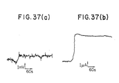
- Fig. 37(a) shows an example of the sensor output in the potential measurement system
- Fig. 37(b) shows an example of the sensor output of the current measurement system.
- glucose concentration was measured with glucose sensor used as enzyme sensor according to the invention, this is by no means limitative, and the invention is applicable as well to sensors for measuring the concentration of other substrate by using other enzymes.
Landscapes
- Chemical & Material Sciences (AREA)
- Chemical Kinetics & Catalysis (AREA)
- Engineering & Computer Science (AREA)
- Materials Engineering (AREA)
- Mechanical Engineering (AREA)
- Metallurgy (AREA)
- Organic Chemistry (AREA)
- Physical Vapour Deposition (AREA)
- Thin Film Transistor (AREA)
Applications Claiming Priority (8)
| Application Number | Priority Date | Filing Date | Title |
|---|---|---|---|
| JP1077814A JPH02258969A (ja) | 1989-03-29 | 1989-03-29 | 疎水性膜を有する基体の製造方法 |
| JP77814/89 | 1989-03-29 | ||
| JP1156603A JPH0321857A (ja) | 1989-06-19 | 1989-06-19 | 酵素センサ及びその製造方法 |
| JP156603/89 | 1989-06-19 | ||
| JP1206136A JPH0368857A (ja) | 1989-08-09 | 1989-08-09 | Isfetセンサ及びその製造方法 |
| JP206136/89 | 1989-08-09 | ||
| JP219040/89 | 1989-08-25 | ||
| JP1219040A JPH0382757A (ja) | 1989-08-25 | 1989-08-25 | 薄膜作製装置 |
Publications (2)
| Publication Number | Publication Date |
|---|---|
| EP0390692A2 true EP0390692A2 (de) | 1990-10-03 |
| EP0390692A3 EP0390692A3 (de) | 1991-10-02 |
Family
ID=27466106
Family Applications (1)
| Application Number | Title | Priority Date | Filing Date |
|---|---|---|---|
| EP19900400864 Withdrawn EP0390692A3 (de) | 1989-03-29 | 1990-03-29 | Verfahren und Vorrichtung zur Herstellung einer Dünnschicht und Sensor |
Country Status (2)
| Country | Link |
|---|---|
| US (1) | US5296122A (de) |
| EP (1) | EP0390692A3 (de) |
Cited By (4)
| Publication number | Priority date | Publication date | Assignee | Title |
|---|---|---|---|---|
| EP0922955A3 (de) * | 1997-12-13 | 2000-10-04 | Eastman Kodak Company | Ionenkonzentrations- und pHmessung |
| EP1559809A3 (de) * | 2000-08-11 | 2005-11-02 | Satis Vacuum Industries Vertriebs - AG | Vorrichtung und Verfahren zur Substratbeschichtung |
| WO2008096186A1 (en) * | 2007-02-06 | 2008-08-14 | Magyar Tudományos Akademia Kemiai Kutatóközpont | Method for improving surface mechanical and tribological properties of thermoplastic technical polymers comprising oxygen and/or halogen heteroatoms |
| CN113789500A (zh) * | 2021-08-04 | 2021-12-14 | 湖北三峡职业技术学院 | 自动调整离子束溅射角和入射角的离子镀装置及方法 |
Families Citing this family (50)
| Publication number | Priority date | Publication date | Assignee | Title |
|---|---|---|---|---|
| US5549874A (en) * | 1992-04-23 | 1996-08-27 | Ebara Corporation | Discharge reactor |
| GB9225270D0 (en) * | 1992-12-03 | 1993-01-27 | Gec Ferranti Defence Syst | Depositing different materials on a substrate |
| US6331273B1 (en) | 1995-04-25 | 2001-12-18 | Discovery Partners International | Remotely programmable matrices with memories |
| US5741462A (en) * | 1995-04-25 | 1998-04-21 | Irori | Remotely programmable matrices with memories |
| US5751629A (en) | 1995-04-25 | 1998-05-12 | Irori | Remotely programmable matrices with memories |
| US6017496A (en) | 1995-06-07 | 2000-01-25 | Irori | Matrices with memories and uses thereof |
| US6329139B1 (en) | 1995-04-25 | 2001-12-11 | Discovery Partners International | Automated sorting system for matrices with memory |
| US6416714B1 (en) | 1995-04-25 | 2002-07-09 | Discovery Partners International, Inc. | Remotely programmable matrices with memories |
| US5874214A (en) | 1995-04-25 | 1999-02-23 | Irori | Remotely programmable matrices with memories |
| RU2155242C2 (ru) * | 1998-01-13 | 2000-08-27 | Институт проблем машиноведения РАН | Устройство для нанесения покрытий в вакууме |
| GB9922110D0 (en) * | 1999-09-17 | 1999-11-17 | Nordiko Ltd | Ion beam vacuum sputtering apparatus and method |
| WO2001073883A2 (en) * | 2000-03-24 | 2001-10-04 | Cymbet Corporation | Low-temperature fabrication of thin-film energy-storage devices |
| US6671561B1 (en) | 2000-05-01 | 2003-12-30 | Biosense Webster, Inc. | Catheter with electrode having hydrogel layer |
| US6475214B1 (en) | 2000-05-01 | 2002-11-05 | Biosense Webster, Inc. | Catheter with enhanced ablation electrode |
| US6291882B1 (en) * | 2000-06-02 | 2001-09-18 | Siliconware Precision Industries Co., Letd. | Packaging process and structure of electronic device |
| GB0030538D0 (en) * | 2000-12-14 | 2001-01-31 | Nordiko Ltd | Apparatus |
| US6748264B2 (en) | 2002-02-04 | 2004-06-08 | Fook Tin Technologies Limited | Body fat analyzer with integral analog measurement electrodes |
| US20070158178A1 (en) * | 2002-07-23 | 2007-07-12 | Tosoh Smd, Inc. | Method and apparatus for deposition of low-k dielectric materials |
| US6906436B2 (en) * | 2003-01-02 | 2005-06-14 | Cymbet Corporation | Solid state activity-activated battery device and method |
| US7294209B2 (en) * | 2003-01-02 | 2007-11-13 | Cymbet Corporation | Apparatus and method for depositing material onto a substrate using a roll-to-roll mask |
| US7603144B2 (en) * | 2003-01-02 | 2009-10-13 | Cymbet Corporation | Active wireless tagging system on peel and stick substrate |
| US20040131760A1 (en) * | 2003-01-02 | 2004-07-08 | Stuart Shakespeare | Apparatus and method for depositing material onto multiple independently moving substrates in a chamber |
| US6800565B2 (en) * | 2003-01-13 | 2004-10-05 | Veeco Instruments, Inc. | Method of forming thin oxidation layer by cluster ion beam |
| TWI235236B (en) * | 2003-05-09 | 2005-07-01 | Univ Chung Yuan Christian | Ion-sensitive circuit |
| JP4361343B2 (ja) * | 2003-10-03 | 2009-11-11 | ダイキン工業株式会社 | 対水接触角の制御方法 |
| US7211351B2 (en) | 2003-10-16 | 2007-05-01 | Cymbet Corporation | Lithium/air batteries with LiPON as separator and protective barrier and method |
| CN1957487A (zh) * | 2004-01-06 | 2007-05-02 | Cymbet公司 | 具有一个或者更多个可限定层的层式阻挡物结构和方法 |
| WO2006040613A1 (en) * | 2004-10-13 | 2006-04-20 | Xenocs | Method of deposition with reduction of contaminants in an ion assist beam and associated apparatus |
| WO2006089134A2 (en) * | 2005-02-15 | 2006-08-24 | Ehd Technology Group, Inc. | Apparatus and method for surface preparation using energetic and reactive cluster beams |
| KR100702010B1 (ko) * | 2005-03-07 | 2007-03-30 | 삼성전자주식회사 | 반사체, 이를 채택하는 기판 처리 장치 및 이를 사용하는기판 처리 방법 |
| US7776478B2 (en) * | 2005-07-15 | 2010-08-17 | Cymbet Corporation | Thin-film batteries with polymer and LiPON electrolyte layers and method |
| US20070012244A1 (en) * | 2005-07-15 | 2007-01-18 | Cymbet Corporation | Apparatus and method for making thin-film batteries with soft and hard electrolyte layers |
| JP2009502011A (ja) * | 2005-07-15 | 2009-01-22 | シンベット・コーポレイション | 軟質および硬質電解質層付き薄膜電池および方法 |
| TWI302197B (en) * | 2006-01-04 | 2008-10-21 | Univ Nat Yunlin Sci & Tech | Reference ph sensor, the preparation and application thereof |
| EP2044610B1 (de) * | 2006-07-20 | 2012-11-28 | SPP Process Technology Systems UK Limited | Plasmaquellen |
| WO2008009898A1 (en) * | 2006-07-20 | 2008-01-24 | Aviza Technology Limited | Ion sources |
| JP5313893B2 (ja) * | 2006-07-20 | 2013-10-09 | エスピーティーエス テクノロジーズ イーティー リミティド | イオンデポジション装置 |
| KR100881954B1 (ko) * | 2007-11-09 | 2009-02-06 | 한국전자통신연구원 | 반응성 스퍼터링 증착 장치 |
| US11996517B2 (en) | 2011-06-29 | 2024-05-28 | Space Charge, LLC | Electrochemical energy storage devices |
| US11527774B2 (en) | 2011-06-29 | 2022-12-13 | Space Charge, LLC | Electrochemical energy storage devices |
| US9853325B2 (en) | 2011-06-29 | 2017-12-26 | Space Charge, LLC | Rugged, gel-free, lithium-free, high energy density solid-state electrochemical energy storage devices |
| US10601074B2 (en) | 2011-06-29 | 2020-03-24 | Space Charge, LLC | Rugged, gel-free, lithium-free, high energy density solid-state electrochemical energy storage devices |
| US10658705B2 (en) | 2018-03-07 | 2020-05-19 | Space Charge, LLC | Thin-film solid-state energy storage devices |
| CN103492112B (zh) * | 2012-04-16 | 2016-08-17 | 株式会社谷黑组 | 焊接装置、焊接方法以及所制造的基板及电子部件 |
| DE102012210183B4 (de) * | 2012-06-18 | 2017-03-23 | Siemens Healthcare Gmbh | Anordnung und Verfahren zur Analyse von Nukleinsäuresequenzen |
| CN103545460B (zh) | 2012-07-10 | 2017-04-12 | 三星显示有限公司 | 有机发光显示装置、有机发光显示设备及其制造方法 |
| KR102211964B1 (ko) * | 2013-08-22 | 2021-02-05 | 삼성디스플레이 주식회사 | 박막 증착 장치 및 그것을 이용한 박막 증착 방법 |
| EP3187863B1 (de) * | 2014-08-29 | 2019-08-07 | Kyocera Corporation | Sensorsubstrat, sensorsubstrat mit einer leitung und sensorvorrichtung |
| CN104605864A (zh) * | 2015-01-23 | 2015-05-13 | 吴晔旻 | 血液透析尿素实时监控传感器 |
| CN115436214B (zh) * | 2022-09-06 | 2025-04-25 | 北京理工大学 | 一种真空目标靶溅射沉积质量的三维检测设备 |
Family Cites Families (15)
| Publication number | Priority date | Publication date | Assignee | Title |
|---|---|---|---|---|
| GB1295465A (de) * | 1969-11-11 | 1972-11-08 | ||
| US4278890A (en) * | 1977-07-01 | 1981-07-14 | The United States Of America As Represented By The United States Department Of Energy | Method and means of directing an ion beam onto an insulating surface for ion implantation or sputtering |
| US4142958A (en) * | 1978-04-13 | 1979-03-06 | Litton Systems, Inc. | Method for fabricating multi-layer optical films |
| DE3176510D1 (en) * | 1980-11-17 | 1987-12-10 | Shimadzu Corp | Reference electrode |
| EP0078636B2 (de) * | 1981-10-23 | 1997-04-02 | MediSense, Inc. | Sensor für Bestandteile einer Flüssigkeitsmischung |
| US4419203A (en) * | 1982-03-05 | 1983-12-06 | International Business Machines Corporation | Apparatus and method for neutralizing ion beams |
| US4877504A (en) * | 1985-03-28 | 1989-10-31 | Honeywell Inc. | Methods for fabricating electro-optically active niobium dioxide (NbO2) |
| JPS6283641A (ja) * | 1985-10-08 | 1987-04-17 | Sharp Corp | 電界効果型半導体センサ |
| JPH0774440B2 (ja) * | 1986-03-17 | 1995-08-09 | 日新電機株式会社 | イオンビ−ムスパツタ装置 |
| DE3625700A1 (de) * | 1986-07-30 | 1988-02-04 | Siemens Ag | Einrichtung zur herstellung und analyse von mehrkomoponentenfilmen |
| JPS6353265A (ja) * | 1986-08-23 | 1988-03-07 | Nissin Electric Co Ltd | イオンビ−ムスパツタリング装置 |
| US4793908A (en) * | 1986-12-29 | 1988-12-27 | Rockwell International Corporation | Multiple ion source method and apparatus for fabricating multilayer optical films |
| GB2208390B (en) * | 1987-08-06 | 1991-03-27 | Plessey Co Plc | Thin film deposition process |
| EP0393188A4 (en) * | 1987-11-24 | 1991-01-02 | Terumo Kabushiki Kaisha | Reference electrode |
| DE3834318A1 (de) * | 1988-10-08 | 1990-04-12 | Leybold Ag | Vorrichtung zum aufbringen dielektrischer oder metallischer werkstoffe |
-
1990
- 1990-03-29 EP EP19900400864 patent/EP0390692A3/de not_active Withdrawn
-
1992
- 1992-02-18 US US07/837,873 patent/US5296122A/en not_active Expired - Lifetime
Cited By (6)
| Publication number | Priority date | Publication date | Assignee | Title |
|---|---|---|---|---|
| EP0922955A3 (de) * | 1997-12-13 | 2000-10-04 | Eastman Kodak Company | Ionenkonzentrations- und pHmessung |
| US6353323B1 (en) | 1997-12-13 | 2002-03-05 | Eastman Kodak Company | Ion concentration and pH measurement |
| EP1559809A3 (de) * | 2000-08-11 | 2005-11-02 | Satis Vacuum Industries Vertriebs - AG | Vorrichtung und Verfahren zur Substratbeschichtung |
| WO2008096186A1 (en) * | 2007-02-06 | 2008-08-14 | Magyar Tudományos Akademia Kemiai Kutatóközpont | Method for improving surface mechanical and tribological properties of thermoplastic technical polymers comprising oxygen and/or halogen heteroatoms |
| CN113789500A (zh) * | 2021-08-04 | 2021-12-14 | 湖北三峡职业技术学院 | 自动调整离子束溅射角和入射角的离子镀装置及方法 |
| CN113789500B (zh) * | 2021-08-04 | 2023-07-25 | 湖北三峡职业技术学院 | 自动调整离子束溅射角和入射角的离子镀装置及方法 |
Also Published As
| Publication number | Publication date |
|---|---|
| EP0390692A3 (de) | 1991-10-02 |
| US5296122A (en) | 1994-03-22 |
Similar Documents
| Publication | Publication Date | Title |
|---|---|---|
| EP0390692A2 (de) | Verfahren und Vorrichtung zur Herstellung einer Dünnschicht und Sensor | |
| Lin et al. | Vacuum-tight thin-layer spectroelectrochemical cell with a doublet platinum gauze working electrode | |
| Yoshida et al. | A mediator-type biosensor as a new approach to biochemical oxygen demand estimation | |
| Gu et al. | Electrochemical deposition of ZnO thin films on Tin‐Coated glasses | |
| US4192720A (en) | Electrodeposition process for forming amorphous silicon | |
| US5200053A (en) | Reference electrode | |
| CN110249225B (zh) | 用于电化学传感器的电极 | |
| Charlier et al. | Local silicon doping as a promoter of patterned electrografting of diazonium for directed surface functionalization | |
| US20030075438A1 (en) | Method and apparatus for providing an electrochemical gas sensor having a porous electrolyte | |
| US20070084996A1 (en) | Method of preventing analyte alteration in diagnostic apparatuses involving contact of liquid and electrode | |
| US3355371A (en) | Method of anodizing a metal in a plasma including connecting said metal in a separate electrical circuit | |
| Aschauer et al. | Surface characterization of thin-film platinum electrodes for biosensors by means of cyclic voltammetry and laser SNMS | |
| Donsanti et al. | Alkali ion intercalation in V2O5: preparation and laboratory characterization of thin films produced by ALD | |
| Godines et al. | Comparative secondary ion mass spectroscopy analysis of solar cell structures grown by pulsed laser ablation and ion sputtering | |
| EP4597093A1 (de) | Elektrode und elektrochemisches messsystem | |
| Kammlott | Preparation of standards for thin film thickness measurements by Energy Dispersive X-ray analysis | |
| Strein et al. | Steady‐State Voltammetry of Catechol and Guaiacol Analogues at Carbon Fiber Microdisk Electrodes Following Laser and Electrochemical Activation Procedures | |
| US20260110657A1 (en) | Electrode and electrochemical measurement system | |
| Siegenthaler et al. | In-situ scanning tunneling microscopy in electrochemistry | |
| JP7365024B2 (ja) | 試料支持体、イオン化方法及び質量分析方法 | |
| US6379986B1 (en) | Method of forming tunnel oxide film for superconducting X-ray sensor element | |
| RU1836487C (ru) | Способ нанесени пленок гидрида металла в вакууме, применение пленки гидрида металла, полученной способом по п.1, и применение субстрата с пленкой гидрида металла, полученной способом по п.1 | |
| Quinn et al. | Studies of the Ag‐Pt Interface Formed by Ag Deposition from Sulfolane Solutions on Thin Film Electrodes | |
| JP2608206B2 (ja) | マイナスイオン感応電界効果トランジスタ | |
| KR20250050226A (ko) | 페로센-기반 산화환원 공중합체 및 이를 이용한 고-감도 전기화학적 바이오센서의 제조 방법 |
Legal Events
| Date | Code | Title | Description |
|---|---|---|---|
| PUAI | Public reference made under article 153(3) epc to a published international application that has entered the european phase |
Free format text: ORIGINAL CODE: 0009012 |
|
| 17P | Request for examination filed |
Effective date: 19900402 |
|
| AK | Designated contracting states |
Kind code of ref document: A2 Designated state(s): BE DE FR SE |
|
| PUAL | Search report despatched |
Free format text: ORIGINAL CODE: 0009013 |
|
| AK | Designated contracting states |
Kind code of ref document: A3 Designated state(s): BE DE FR SE |
|
| 17Q | First examination report despatched |
Effective date: 19930630 |
|
| STAA | Information on the status of an ep patent application or granted ep patent |
Free format text: STATUS: THE APPLICATION IS DEEMED TO BE WITHDRAWN |
|
| 18D | Application deemed to be withdrawn |
Effective date: 19941025 |