EP0391359A2 - Dispositif photosensible - Google Patents
Dispositif photosensible Download PDFInfo
- Publication number
- EP0391359A2 EP0391359A2 EP90106380A EP90106380A EP0391359A2 EP 0391359 A2 EP0391359 A2 EP 0391359A2 EP 90106380 A EP90106380 A EP 90106380A EP 90106380 A EP90106380 A EP 90106380A EP 0391359 A2 EP0391359 A2 EP 0391359A2
- Authority
- EP
- European Patent Office
- Prior art keywords
- light receiving
- detecting device
- photo detecting
- photoelectric converting
- converting element
- Prior art date
- Legal status (The legal status is an assumption and is not a legal conclusion. Google has not performed a legal analysis and makes no representation as to the accuracy of the status listed.)
- Granted
Links
- 239000004065 semiconductor Substances 0.000 claims abstract description 14
- 239000003990 capacitor Substances 0.000 claims description 14
- 230000008878 coupling Effects 0.000 claims description 12
- 238000010168 coupling process Methods 0.000 claims description 12
- 238000005859 coupling reaction Methods 0.000 claims description 12
- 230000003287 optical effect Effects 0.000 description 19
- 238000006243 chemical reaction Methods 0.000 description 4
- 230000009467 reduction Effects 0.000 description 3
- 238000000034 method Methods 0.000 description 2
- 230000003321 amplification Effects 0.000 description 1
- 230000008859 change Effects 0.000 description 1
- 238000010586 diagram Methods 0.000 description 1
- 230000006872 improvement Effects 0.000 description 1
- 238000003199 nucleic acid amplification method Methods 0.000 description 1
- 230000008569 process Effects 0.000 description 1
Images

Classifications
-
- G—PHYSICS
- G11—INFORMATION STORAGE
- G11B—INFORMATION STORAGE BASED ON RELATIVE MOVEMENT BETWEEN RECORD CARRIER AND TRANSDUCER
- G11B7/00—Recording or reproducing by optical means, e.g. recording using a thermal beam of optical radiation by modifying optical properties or the physical structure, reproducing using an optical beam at lower power by sensing optical properties; Record carriers therefor
- G11B7/12—Heads, e.g. forming of the optical beam spot or modulation of the optical beam
- G11B7/13—Optical detectors therefor
- G11B7/131—Arrangement of detectors in a multiple array
-
- G—PHYSICS
- G11—INFORMATION STORAGE
- G11B—INFORMATION STORAGE BASED ON RELATIVE MOVEMENT BETWEEN RECORD CARRIER AND TRANSDUCER
- G11B7/00—Recording or reproducing by optical means, e.g. recording using a thermal beam of optical radiation by modifying optical properties or the physical structure, reproducing using an optical beam at lower power by sensing optical properties; Record carriers therefor
- G11B7/08—Disposition or mounting of heads or light sources relatively to record carriers
- G11B7/09—Disposition or mounting of heads or light sources relatively to record carriers with provision for moving the light beam or focus plane for the purpose of maintaining alignment of the light beam relative to the record carrier during transducing operation, e.g. to compensate for surface irregularities of the latter or for track following
- G11B7/0901—Disposition or mounting of heads or light sources relatively to record carriers with provision for moving the light beam or focus plane for the purpose of maintaining alignment of the light beam relative to the record carrier during transducing operation, e.g. to compensate for surface irregularities of the latter or for track following for track following only
- G11B7/0903—Multi-beam tracking systems
Definitions
- the present invention relates to a photo detecting device used in an optical pickup for an optical disk apparatus and the like and, more specifically, to an improvement of a photo detecting device including a photoelectric conversion device and the signal processing circuit formed on the same semiconductor chip.
- An optical pickup used in a conventional optical disk apparatus comprises a photoelectric conversion device formed on a semiconductor chip for receiving light reflected from a recording medium to convert the same into electric signals.
- the electric signals outputted from such a photoelectric conversion device are subjected to processes such as arithmetic amplification in a signal processing circuit out of the semiconductor chip to be converted into information reproducing signals, focus error signals and tracking error signals.
- Recent technique of integrated circuits has developed an OPIC (Optical Integrated Circuit) photo detecting device in which the signal processing circuit as well as the photoelectric conversion device are formed on one semiconductor chip, which has made simple the design of the signal processing circuit.
- OPIC Optical Integrated Circuit
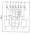
- Fig. 4 shows one example of the conventional OPIC photo detecting device.
- the photo detecting device comprises three photoelectric converting elements 11, 12 and 13.
- the central photoelectric converting element 11 has four divided light receiving regions 11a, 11b, 11c and 11d.
- the output signals from the light receiving regions 11a to 11b are connected to minus input terminals of differential amplifiers A11, A12, A13 and A14, respectively, and to an input terminal of an amplifier A15 through coupling capacitors C11, C12, C13 and C14.
- the differential amplifiers A11 to A14 have their plus input terminals all grounded.
- the photo electric converting elements 12 and 13 on both ends are connected to minus input terminals of the differential amplifiers A16 and A17, respectively.
- the differential amplifiers A16 and A17 have their plus input terminals grounded.
- the signals Sa to Sd outputted from the light receiving regions 11a to 11d have their fluctuation of low frequency components removed through coupling capacitors C11 to C14, and thereafter they are added to each other.
- a reproduction signal RF is provided by amplifying the summed signal (Sa + Sb + Sc + Sd) by the amplifier A15.
- signals Se and Sf outputted from the photoelectric converting elements 12 and 13 on both ends are amplified by the differential amplifiers A16 and A17, respectively, to be externally outputted, and the tracking error signal TES is provided by a subtracting operation by an external circuit.
- a plurality of operational amplifiers must be provided in the external circuit for obtaining the focus error signal FES. It is difficult to provide the same characteristics to all of these plurality of operational amplifiers in the external circuit. Accordingly, when the ambient temperature changes, an offset voltage tends to be generated in the focus error signal FES obtained from the external circuit at the in-focus state. The offset voltage prevents accurate focus control.
- the photoelectric converting element 11 at the center comprises four light receiving regions 11a to 11d, four output terminals are necessary to take out signals Sa to Sd to the outside from the light receiving regions. This increases the number of the output terminals of the photo detecting device itself, which makes it difficult to reduce the size of the photo detecting device.
- an object of the present invention is to provide a photo detecting device which is compact and in which an offset voltage in a focus error signal is hardly generated.
- the photo detecting device comprises a photoelectric converting element formed on a semiconductor chip, the photoelectric converting element being divided into first and second light receiving regions, and a signal processing circuit formed on the same semiconductor chip, with the signal processing circuit having subtracting means for subtracting an output signal from the second light receiving region from the output signal from the first light receiving region.
- the photo detecting device comprises first and second photoelectric converting elements formed on the semiconductor chip, the first photoelectric converting element being divided into first and second light receiving regions, and a signal processing circuit formed on the same semiconductor chip, the signal processing circuit having subtracting means for subtracting the output signal from the second light receiving region from the output signal of the first light receiving region, and first and second capacitor means for coupling the output from the first and second light receiving regions with output of the second photoelectric converting element, respectively.
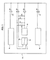
- the photo detecting device 5 comprises four photoelectric converting elements 7, 8, 9 and 10.
- the photoelectric converting element 7 is divided into two light receiving regions 7a and 7b.
- An output signal from the light receiving region 7a is connected to a plus input terminal of a differential amplifier A1 serving as a subtracting means, and an output signal of the other light receiving region 7b is connected to a minus input terminal of the same differential amplifier A1.
- An output signal from the photoelectric converting element 8 formed of a single light receiving region is connected to an input terminal of an amplifier A2.
- the light receiving region 7a is further connected to an input terminal of the amplifier A2 through a coupling capacitor C1 and a resistance R1 parallel to the coupling capacitor C1.
- the other light receiving region 7b is connected to the input terminal of the amplifier A2 through a coupling capacitor C2 and a resistance R2 parallel to the coupling capacitor C2.
- Output terminals of the differential amplifier A1 and of the amplifier A2 are drawn to the outside as outputs of the photc detecting device 5.
- Output signals of the remaining photoelectric converting elements 9 and 10 are connected to minus input terminals of differential amplifiers A3 and A4.
- the differential amplifiers A3 and A4 have their plus input terminals grounded.
- the output terminals of the differential amplifiers A3 and A4 are drawn to the outside as outputs of the photo detecting device 5.
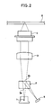
- Fig. 2 shows main components of a hologram type optical pickup using the photo detecting device of Fig. 1.
- the principle of operation of the hologram type optical pickup is disclosed in detail in United States Patent No. 4,835,378, for instance.
- an optical beam emitted from a light source 1 is divided into three sub beams along a line by a diffraction grating 2a below a diffracting apparatus 2.
- the sub beams are converted into parallel sub beams by a collimator lens 3.
- the parallel sub beams are focused on an information surface of a disk 6 by an objective lens.
- the three reflected beams from the disk 6 enter the objective lens 4 and pass through the collimator lens 3.
- each of the three reflected beams which passed through the collimator lens 3 are diffracted toward the photo detecting device 5 by a diffraction grating 2b above the diffracting apparatus 2.
- each of the three reflected beams along one line is divided into two sub beams. Namely, one of the sub beams divided from the central reflected beam, used for reading recorded information and for focusing, enters the photoelectric converting element 7, and the other sub beam enters the photoelectric converting element 8.
- Two sub beams divided from one of the reflected beams on both ends used for tracking both enter the photoelectric converting element 9.
- Two sub beams divided from the other one of the reflected beams on both sides both enter the photoelectric converting element 10.
- Figs. 3A, 3B and 3C show a relation between focusing and the state of the optical beam spot projected on the photoelectric converting element 7.
- the optical spot P is a small circle crossing the boundary between two light receiving regions 7a and 7b, as shown in Fig. 3B.
- the optical spot P becomes an enlarged semicircle on the light receiving region 7b, as shown in Fig. 3A.
- the optical spot P become an enlarged semicircle on the light receiving region 7a, as shown in Fig. 3C.
- the difference between outputs from the light receiving regions 7a and 7b can be used as a focus error signal corresponding to deviation of the information recording surface of the disk 6 from the in-focus position.
- the reflected sub beam projected on the light receiving regions 7a and 7b are converted into signals of the magnitudes corresponding to the intensity of light received by the light receiving regions 7a and 7b to be outputted, respectively, and thereafter the output signal from the light receiving region 7b is subtracted from the output signal from the light receiving region 7a by the differential amplifier A12.
- the focus error signal provided by this subtraction is externally outputted.
- the output signals from the light receiving regions 7a and 7b with the low frequency component thereof removed by coupling capacitors C1 and C2 are added to the output signal from the photoelectric converting element 8.
- the summed signal is amplified by the amplifier A2 to be externally outputted as a reproduction signal.
- DC component of the output signals from the light receiving regions 7a and 7b are added to the DC component of the output signal from the photoelectric converting element 8 through the resistances R1 and R2, and the added DC components are also detected.
- the DC components are used for distinguishing the information surface and the protection surface of the optical disk.
- the output signals of the photoelectric converting elements 9 and 10 are amplified by differential amplifiers A3 and A4, respectively, to be outputted.
- the signals amplified by the differential amplifiers A3 and A4 are subtracted by an external circuit (not shown), to be used as the tracking error signal.
- the focus error signal can be provided by arithmetic operation in the photo detecting device. Therefore, generation of an offset voltage in the focus error signal derived from the change in ambient temperature can be suppressed.
- the number of output terminals for the focus error signal outputted outside of the photo detecting device is 1, and the reduction of the number of the output terminal enables reduction of the photo detecting device in size.
- the focus error signal is calculated in the photo detecting device, a circuit for calculating the focus error signal can be removed from the external circuit. Accordingly, when the photo detecting device is used built in the optical pickup, the design of the external circuit can be simplified.
- the ratio of the area occupied by the coupling capacitors to the total area of the photo detecting device becomes smaller, which further reduces the size of the photo detecting device.
Landscapes
- Physics & Mathematics (AREA)
- Optics & Photonics (AREA)
- Optical Recording Or Reproduction (AREA)
- Optical Head (AREA)
- Solid State Image Pick-Up Elements (AREA)
Applications Claiming Priority (2)
| Application Number | Priority Date | Filing Date | Title |
|---|---|---|---|
| JP89315/89 | 1989-04-07 | ||
| JP1089315A JPH0785310B2 (ja) | 1989-04-07 | 1989-04-07 | 信号処理回路内蔵型受光素子 |
Publications (3)
| Publication Number | Publication Date |
|---|---|
| EP0391359A2 true EP0391359A2 (fr) | 1990-10-10 |
| EP0391359A3 EP0391359A3 (fr) | 1992-08-19 |
| EP0391359B1 EP0391359B1 (fr) | 1995-06-28 |
Family
ID=13967234
Family Applications (1)
| Application Number | Title | Priority Date | Filing Date |
|---|---|---|---|
| EP90106380A Expired - Lifetime EP0391359B1 (fr) | 1989-04-07 | 1990-04-03 | Dispositif photosensible |
Country Status (4)
| Country | Link |
|---|---|
| US (1) | US5049733A (fr) |
| EP (1) | EP0391359B1 (fr) |
| JP (1) | JPH0785310B2 (fr) |
| DE (1) | DE69020401T2 (fr) |
Cited By (3)
| Publication number | Priority date | Publication date | Assignee | Title |
|---|---|---|---|---|
| EP1209447A3 (fr) * | 2000-11-27 | 2004-03-17 | Omron Corporation | Détecteur de lumière et carte de détection de la lumière à puce associée |
| EP2831586A4 (fr) * | 2012-03-26 | 2016-02-17 | Xcellcure Llc | Dispositif et procédé pour la détection d'analysats |
| US10746745B2 (en) | 2007-09-10 | 2020-08-18 | Academisch Ziekenhuis Leiden | Future cardiac event biomarkers CCL3, CCL5, and CCL18 |
Families Citing this family (6)
| Publication number | Priority date | Publication date | Assignee | Title |
|---|---|---|---|---|
| JP2621537B2 (ja) * | 1990-02-07 | 1997-06-18 | 松下電器産業株式会社 | 光電流電圧変換器及び光ディスク記録/再生装置 |
| DE4017487A1 (de) * | 1990-05-31 | 1991-12-05 | Thomson Brandt Gmbh | Servoregelkreis |
| JPH04313818A (ja) * | 1991-01-30 | 1992-11-05 | Pioneer Electron Corp | アクチュエータ位置検出装置、アクチュエータ位置制御装置及びトラックサーチ制御装置 |
| US6559488B1 (en) * | 2000-10-02 | 2003-05-06 | Stmicroelectronics, Inc. | Integrated photodetector |
| US6580109B1 (en) | 2002-02-01 | 2003-06-17 | Stmicroelectronics, Inc. | Integrated circuit device including two types of photodiodes |
| US6743652B2 (en) * | 2002-02-01 | 2004-06-01 | Stmicroelectronics, Inc. | Method for making an integrated circuit device including photodiodes |
Family Cites Families (7)
| Publication number | Priority date | Publication date | Assignee | Title |
|---|---|---|---|---|
| US4737946A (en) * | 1984-09-03 | 1988-04-12 | Omron Tateisi Electronics Co. | Device for processing optical data with improved optical allignment means |
| JPS61117737A (ja) * | 1984-11-13 | 1986-06-05 | Pioneer Electronic Corp | フオ−カスサ−ボ装置 |
| US4797868A (en) * | 1985-05-15 | 1989-01-10 | Kabushiki Kaisha Toshiba | Optical system employing a laser beam for focusing, tracking and transferring information signals with respect to a magneto-optical memory |
| DE3665372D1 (en) * | 1985-05-31 | 1989-10-05 | Siemens Ag | Optical system for guiding the read-out beam in a magneto-optical memory |
| DE3715491A1 (de) * | 1987-05-09 | 1988-11-17 | Thomson Brandt Gmbh | Geraet zur wiedergabe von daten |
| NL8702245A (nl) * | 1987-09-21 | 1989-04-17 | Philips Nv | Inrichting voor het met optische straling aftasten van een stralingsreflekterend informatievlak. |
| JPH01151022A (ja) * | 1987-12-09 | 1989-06-13 | Sharp Corp | 光ピックアップ装置 |
-
1989
- 1989-04-07 JP JP1089315A patent/JPH0785310B2/ja not_active Expired - Fee Related
-
1990
- 1990-04-03 DE DE69020401T patent/DE69020401T2/de not_active Expired - Fee Related
- 1990-04-03 EP EP90106380A patent/EP0391359B1/fr not_active Expired - Lifetime
- 1990-04-04 US US07/504,672 patent/US5049733A/en not_active Expired - Lifetime
Cited By (9)
| Publication number | Priority date | Publication date | Assignee | Title |
|---|---|---|---|---|
| EP1209447A3 (fr) * | 2000-11-27 | 2004-03-17 | Omron Corporation | Détecteur de lumière et carte de détection de la lumière à puce associée |
| US10746745B2 (en) | 2007-09-10 | 2020-08-18 | Academisch Ziekenhuis Leiden | Future cardiac event biomarkers CCL3, CCL5, and CCL18 |
| EP2831586A4 (fr) * | 2012-03-26 | 2016-02-17 | Xcellcure Llc | Dispositif et procédé pour la détection d'analysats |
| US9958457B2 (en) | 2012-03-26 | 2018-05-01 | Xcellcure, Llc | Device and method for detection of analytes |
| CN108226482A (zh) * | 2012-03-26 | 2018-06-29 | 埃克塞尔柯尔有限责任公司 | 用于检测分析物的装置和方法 |
| US10564166B2 (en) | 2012-03-26 | 2020-02-18 | Xcellcure, Llc | Device and method for detection of analytes |
| EP3968026A1 (fr) * | 2012-03-26 | 2022-03-16 | XCellCure, LLC | Dispositif et procédé de détection d'analytes |
| US11802880B2 (en) | 2012-03-26 | 2023-10-31 | Xcellcure, Llc | Device and method for detection of analytes |
| US12292449B2 (en) | 2012-03-26 | 2025-05-06 | Xcellcure, Llc | Device and method for detection of analytes |
Also Published As
| Publication number | Publication date |
|---|---|
| JPH02267743A (ja) | 1990-11-01 |
| US5049733A (en) | 1991-09-17 |
| JPH0785310B2 (ja) | 1995-09-13 |
| DE69020401D1 (de) | 1995-08-03 |
| DE69020401T2 (de) | 1996-03-21 |
| EP0391359A3 (fr) | 1992-08-19 |
| EP0391359B1 (fr) | 1995-06-28 |
Similar Documents
| Publication | Publication Date | Title |
|---|---|---|
| KR100252600B1 (ko) | 광픽업장치,광디스크기록재생장치및포커스오차신호생성방법 | |
| JPH01269239A (ja) | 光ピックアップ装置 | |
| KR100749001B1 (ko) | 광픽업장치 | |
| EP0391359B1 (fr) | Dispositif photosensible | |
| US4658391A (en) | Focus error detection device for an optical recording/playing back system | |
| US5287338A (en) | Error signal generation for light beam reflected from optical disk with plurality of light detecting elements | |
| EP0478222B1 (fr) | Tête de lecture optique avec un élément optique holographique | |
| JPH01253841A (ja) | ホログラムを用いた受光装置及び光ヘッド装置 | |
| JPH07272303A (ja) | 光ディスク装置、光学ピックアップ及び光学ピックアップの組立方法 | |
| US7057146B2 (en) | Optical pickup having a diffraction grating and a hologram element | |
| JP3289872B2 (ja) | トラツキングエラー検出方法 | |
| JP2003281749A5 (fr) | ||
| JP2000123398A (ja) | 光ピックアップ装置 | |
| JPS5984352A (ja) | 焦点誤差検出装置 | |
| KR100247956B1 (ko) | 광픽업장치 | |
| KR200172921Y1 (ko) | 홀로그램소자를 채용한 광픽업 장치 | |
| WO2004025635A1 (fr) | Dispositif de lecture optique | |
| JPS63249940A (ja) | 光ピツクアツプの対物レンズ位置検出装置 | |
| KR19980029873A (ko) | 광 픽-업장치 | |
| JP2002358669A (ja) | 光ピックアップモジュールおよび光ディスク装置 | |
| HU209536B (en) | Circuit arrangement for suppressing disturbing high frequency signal component superimposed on the servo signals | |
| KR19990012971A (ko) | 광픽업의 트랙킹 오차 신호 생성방법 및 장치 | |
| JPH04255923A (ja) | 光ピックアップ | |
| JPS63263636A (ja) | 光学的情報再生装置 | |
| JPH04344333A (ja) | 光学ピックアップ装置 |
Legal Events
| Date | Code | Title | Description |
|---|---|---|---|
| PUAI | Public reference made under article 153(3) epc to a published international application that has entered the european phase |
Free format text: ORIGINAL CODE: 0009012 |
|
| 17P | Request for examination filed |
Effective date: 19900403 |
|
| AK | Designated contracting states |
Kind code of ref document: A2 Designated state(s): DE GB |
|
| PUAL | Search report despatched |
Free format text: ORIGINAL CODE: 0009013 |
|
| AK | Designated contracting states |
Kind code of ref document: A3 Designated state(s): DE GB |
|
| 17Q | First examination report despatched |
Effective date: 19931207 |
|
| GRAA | (expected) grant |
Free format text: ORIGINAL CODE: 0009210 |
|
| AK | Designated contracting states |
Kind code of ref document: B1 Designated state(s): DE GB |
|
| REF | Corresponds to: |
Ref document number: 69020401 Country of ref document: DE Date of ref document: 19950803 |
|
| PLBE | No opposition filed within time limit |
Free format text: ORIGINAL CODE: 0009261 |
|
| STAA | Information on the status of an ep patent application or granted ep patent |
Free format text: STATUS: NO OPPOSITION FILED WITHIN TIME LIMIT |
|
| 26N | No opposition filed | ||
| REG | Reference to a national code |
Ref country code: GB Ref legal event code: IF02 |
|
| PGFP | Annual fee paid to national office [announced via postgrant information from national office to epo] |
Ref country code: GB Payment date: 20040331 Year of fee payment: 15 |
|
| PGFP | Annual fee paid to national office [announced via postgrant information from national office to epo] |
Ref country code: DE Payment date: 20040415 Year of fee payment: 15 |
|
| PG25 | Lapsed in a contracting state [announced via postgrant information from national office to epo] |
Ref country code: GB Free format text: LAPSE BECAUSE OF NON-PAYMENT OF DUE FEES Effective date: 20050403 |
|
| PG25 | Lapsed in a contracting state [announced via postgrant information from national office to epo] |
Ref country code: DE Free format text: LAPSE BECAUSE OF NON-PAYMENT OF DUE FEES Effective date: 20051101 |
|
| GBPC | Gb: european patent ceased through non-payment of renewal fee |
Effective date: 20050403 |