EP0394678A2 - Panneaux à circuits multicouches pour conducteurs minces et procédé pour leur production - Google Patents
Panneaux à circuits multicouches pour conducteurs minces et procédé pour leur production Download PDFInfo
- Publication number
- EP0394678A2 EP0394678A2 EP90105640A EP90105640A EP0394678A2 EP 0394678 A2 EP0394678 A2 EP 0394678A2 EP 90105640 A EP90105640 A EP 90105640A EP 90105640 A EP90105640 A EP 90105640A EP 0394678 A2 EP0394678 A2 EP 0394678A2
- Authority
- EP
- European Patent Office
- Prior art keywords
- circuit boards
- printed circuit
- layer
- multilayer printed
- multilayer
- Prior art date
- Legal status (The legal status is an assumption and is not a legal conclusion. Google has not performed a legal analysis and makes no representation as to the accuracy of the status listed.)
- Withdrawn
Links
- 239000004020 conductor Substances 0.000 title claims abstract description 12
- 238000000034 method Methods 0.000 title claims description 21
- 229920002620 polyvinyl fluoride Polymers 0.000 claims abstract description 5
- 239000004744 fabric Substances 0.000 claims abstract 2
- 239000011521 glass Substances 0.000 claims abstract 2
- RYGMFSIKBFXOCR-UHFFFAOYSA-N Copper Chemical compound [Cu] RYGMFSIKBFXOCR-UHFFFAOYSA-N 0.000 claims description 15
- 238000001465 metallisation Methods 0.000 claims description 9
- 229910052802 copper Inorganic materials 0.000 claims description 7
- 239000010949 copper Substances 0.000 claims description 7
- 239000003795 chemical substances by application Substances 0.000 claims description 5
- 239000000654 additive Substances 0.000 claims description 4
- 230000000996 additive effect Effects 0.000 claims description 2
- 230000008961 swelling Effects 0.000 claims description 2
- PXHVJJICTQNCMI-UHFFFAOYSA-N Nickel Chemical compound [Ni] PXHVJJICTQNCMI-UHFFFAOYSA-N 0.000 description 12
- 239000011889 copper foil Substances 0.000 description 9
- 238000005530 etching Methods 0.000 description 7
- 238000004519 manufacturing process Methods 0.000 description 7
- 229910052751 metal Inorganic materials 0.000 description 6
- 239000002184 metal Substances 0.000 description 6
- 229910052759 nickel Inorganic materials 0.000 description 6
- 239000003822 epoxy resin Substances 0.000 description 4
- 229920000647 polyepoxide Polymers 0.000 description 4
- ATJFFYVFTNAWJD-UHFFFAOYSA-N Tin Chemical compound [Sn] ATJFFYVFTNAWJD-UHFFFAOYSA-N 0.000 description 3
- 238000000151 deposition Methods 0.000 description 3
- 238000011161 development Methods 0.000 description 3
- 230000018109 developmental process Effects 0.000 description 3
- 238000003384 imaging method Methods 0.000 description 3
- 239000011135 tin Substances 0.000 description 3
- SPEUIVXLLWOEMJ-UHFFFAOYSA-N 1,1-dimethoxyethane Chemical compound COC(C)OC SPEUIVXLLWOEMJ-UHFFFAOYSA-N 0.000 description 2
- IAZDPXIOMUYVGZ-UHFFFAOYSA-N Dimethylsulphoxide Chemical compound CS(C)=O IAZDPXIOMUYVGZ-UHFFFAOYSA-N 0.000 description 2
- KDLHZDBZIXYQEI-UHFFFAOYSA-N Palladium Chemical compound [Pd] KDLHZDBZIXYQEI-UHFFFAOYSA-N 0.000 description 2
- KRVSOGSZCMJSLX-UHFFFAOYSA-L chromic acid Substances O[Cr](O)(=O)=O KRVSOGSZCMJSLX-UHFFFAOYSA-L 0.000 description 2
- 239000011888 foil Substances 0.000 description 2
- AWJWCTOOIBYHON-UHFFFAOYSA-N furo[3,4-b]pyrazine-5,7-dione Chemical compound C1=CN=C2C(=O)OC(=O)C2=N1 AWJWCTOOIBYHON-UHFFFAOYSA-N 0.000 description 2
- 230000035784 germination Effects 0.000 description 2
- 239000011133 lead Substances 0.000 description 2
- 238000003825 pressing Methods 0.000 description 2
- 229910000679 solder Inorganic materials 0.000 description 2
- SLPUTJFVMJPMKV-UHFFFAOYSA-N 1-methylpyrrolidin-3-one Chemical compound CN1CCC(=O)C1 SLPUTJFVMJPMKV-UHFFFAOYSA-N 0.000 description 1
- QPLDLSVMHZLSFG-UHFFFAOYSA-N Copper oxide Chemical compound [Cu]=O QPLDLSVMHZLSFG-UHFFFAOYSA-N 0.000 description 1
- 239000005751 Copper oxide Substances 0.000 description 1
- FXHOOIRPVKKKFG-UHFFFAOYSA-N N,N-Dimethylacetamide Chemical compound CN(C)C(C)=O FXHOOIRPVKKKFG-UHFFFAOYSA-N 0.000 description 1
- 239000007864 aqueous solution Substances 0.000 description 1
- 239000011248 coating agent Substances 0.000 description 1
- 238000000576 coating method Methods 0.000 description 1
- 230000001143 conditioned effect Effects 0.000 description 1
- 238000010276 construction Methods 0.000 description 1
- 229910000431 copper oxide Inorganic materials 0.000 description 1
- -1 dimethylformammide Chemical compound 0.000 description 1
- 238000005553 drilling Methods 0.000 description 1
- PCHJSUWPFVWCPO-UHFFFAOYSA-N gold Chemical compound [Au] PCHJSUWPFVWCPO-UHFFFAOYSA-N 0.000 description 1
- 229910052737 gold Inorganic materials 0.000 description 1
- 239000010931 gold Substances 0.000 description 1
- 150000002739 metals Chemical class 0.000 description 1
- 238000006386 neutralization reaction Methods 0.000 description 1
- 239000012457 nonaqueous media Substances 0.000 description 1
- 239000007800 oxidant agent Substances 0.000 description 1
- 230000001590 oxidative effect Effects 0.000 description 1
- 238000012856 packing Methods 0.000 description 1
- 229910052763 palladium Inorganic materials 0.000 description 1
- 230000001681 protective effect Effects 0.000 description 1
- 238000007788 roughening Methods 0.000 description 1
- 238000007650 screen-printing Methods 0.000 description 1
- 238000005476 soldering Methods 0.000 description 1
- 239000000243 solution Substances 0.000 description 1
- 239000000126 substance Substances 0.000 description 1
- 238000004065 wastewater treatment Methods 0.000 description 1
Images


Classifications
-
- H—ELECTRICITY
- H05—ELECTRIC TECHNIQUES NOT OTHERWISE PROVIDED FOR
- H05K—PRINTED CIRCUITS; CASINGS OR CONSTRUCTIONAL DETAILS OF ELECTRIC APPARATUS; MANUFACTURE OF ASSEMBLAGES OF ELECTRICAL COMPONENTS
- H05K3/00—Apparatus or processes for manufacturing printed circuits
- H05K3/46—Manufacturing multilayer circuits
- H05K3/4644—Manufacturing multilayer circuits by building the multilayer layer by layer, i.e. build-up multilayer circuits
- H05K3/4661—Adding a circuit layer by direct wet plating, e.g. electroless plating; insulating materials adapted therefor
-
- H—ELECTRICITY
- H05—ELECTRIC TECHNIQUES NOT OTHERWISE PROVIDED FOR
- H05K—PRINTED CIRCUITS; CASINGS OR CONSTRUCTIONAL DETAILS OF ELECTRIC APPARATUS; MANUFACTURE OF ASSEMBLAGES OF ELECTRICAL COMPONENTS
- H05K3/00—Apparatus or processes for manufacturing printed circuits
- H05K3/46—Manufacturing multilayer circuits
- H05K3/4611—Manufacturing multilayer circuits by laminating two or more circuit boards
- H05K3/4626—Manufacturing multilayer circuits by laminating two or more circuit boards characterised by the insulating layers or materials
-
- H—ELECTRICITY
- H05—ELECTRIC TECHNIQUES NOT OTHERWISE PROVIDED FOR
- H05K—PRINTED CIRCUITS; CASINGS OR CONSTRUCTIONAL DETAILS OF ELECTRIC APPARATUS; MANUFACTURE OF ASSEMBLAGES OF ELECTRICAL COMPONENTS
- H05K2201/00—Indexing scheme relating to printed circuits covered by H05K1/00
- H05K2201/01—Dielectrics
- H05K2201/0137—Materials
- H05K2201/015—Fluoropolymer, e.g. polytetrafluoroethylene [PTFE]
-
- H—ELECTRICITY
- H05—ELECTRIC TECHNIQUES NOT OTHERWISE PROVIDED FOR
- H05K—PRINTED CIRCUITS; CASINGS OR CONSTRUCTIONAL DETAILS OF ELECTRIC APPARATUS; MANUFACTURE OF ASSEMBLAGES OF ELECTRICAL COMPONENTS
- H05K2203/00—Indexing scheme relating to apparatus or processes for manufacturing printed circuits covered by H05K3/00
- H05K2203/06—Lamination
- H05K2203/068—Features of the lamination press or of the lamination process, e.g. using special separator sheets
Definitions
- the invention relates to multilayer printed circuit boards for fine conductors and methods for their production.
- the multilayer printed circuit boards according to the invention are intended to enable the further development of such printed circuit boards into finer conductor track widths.
- a prepreg surface that is smooth in the micro range and free of impressions should be ensured.
- Multi-layer circuit boards are already known. These represent further developments of printed circuits in order to enable higher packing densities and better connections of the electrical components. According to the state of the art, multilayer printed circuit boards have one or more inner layers, depending on the number of circuit levels, which are connected to one another either by one another or by covering with protective and pressure foils by pressing under pressure and temperature.
- one or two prepregs are placed between the inner layers and between a copper foil that closes to the outside.
- a copper foil that closes to the outside.
- it is a specially prepared copper foil of 35 ⁇ or 17.5 ⁇ , with which the adhesion or peeling properties of the conductor tracks and metallized surfaces are achieved.
- the object of the invention is to provide multilayer printed circuit boards which are free of copper foils.
- the multilayer printed circuit boards according to the invention have the advantage of eliminating the outer layers of copper foils compared to the prior art.
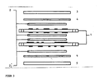
- a further advantage lies in the use of a polyvinyl fluoride film which, in conjunction with the intermediate plates in the construction of the press package, ensures a prepreg surface which is smooth in the micro range and free of impressions.
- the polyvinyl fluoride film also acts as a release agent between the prepreg and intermediate plate and ensures the removal of the pressed multilayer from the pressing tool.
- This press package is combined with other press packages, which are separated from one another by intermediate plates, in a press tool and pressed according to known processes.
- the holes provided for receiving component connecting pins or for plated-through holes are preferably made before the metallization, which are then pretreated, germinated and metallized together with the outer surfaces.
- One embodiment consists in first subjecting the epoxy resin surface to an oxidative roughening step using etching agents such as chromic acid, a chromic acid-containing agent or permanganate solutions.
- etching agents such as chromic acid, a chromic acid-containing agent or permanganate solutions.
- the epoxy resin surface can preferably first be brought into contact with an organic swelling agent, such as, for example, dimethyl sulfoxide, 1-methyl-3-pyrrolidone, dimethylacetamide, dimethylformammide, dimethylacetal or other aqueous or non-aqueous solutions.
- an organic swelling agent such as, for example, dimethyl sulfoxide, 1-methyl-3-pyrrolidone, dimethylacetamide, dimethylformammide, dimethylacetal or other aqueous or non-aqueous solutions.
- a neutralization or reduction step is preferably connected to remove residual oxidants that are still adhering.
- the usual way is conditioned, germinated and
- an imaging process such as screen printing or a phototechnical process in negative technique
- the metallization then takes place exclusively at the locations specified by the imaging process, where conductor track structures or soldering locations are desired.
- Metal deposition takes place in the conventional autocatalytically depositing metallization baths, preferably electrolessly depositing copper baths, up to the desired final layer thickness.
- an autocatalytically depositing metallization bath for example a copper or nickel bath.
- This first metal film can then be further reinforced in a galvanic metallization bath. This gives, for example, a 3-5 ⁇ m thick metal coating, which is subsequently subjected to an imaging process, so that the later conductor or solder joint structures are produced using the negative process.
- the conductive pattern is then expanded in the galvanoresist channels in a galvanically working bath to the final metal layer thickness.
- copper or nickel can be used as metals.
- the metal parts that were built up thinly are removed by differential etching.
- an etching resist can be applied galvanically or without current before the removal of the galvanoresist.
- Tin / lead, tin, lead, nickel, nickel / gold, palladium / nickel layers or their layer combinations can be used.
- the exposed copper layer is oxidized to copper oxide as the final layer in order to produce black or brown oxide.
- tin can also be used without current.
Landscapes
- Engineering & Computer Science (AREA)
- Manufacturing & Machinery (AREA)
- Microelectronics & Electronic Packaging (AREA)
- Production Of Multi-Layered Print Wiring Board (AREA)
- Laminated Bodies (AREA)
- Manufacturing Of Printed Wiring (AREA)
Applications Claiming Priority (2)
| Application Number | Priority Date | Filing Date | Title |
|---|---|---|---|
| DE3914727 | 1989-04-28 | ||
| DE19893914727 DE3914727A1 (de) | 1989-04-28 | 1989-04-28 | Mehrlagen-leiterplatten fuer feinleiter und verfahren zu ihrer herstellung |
Publications (2)
| Publication Number | Publication Date |
|---|---|
| EP0394678A2 true EP0394678A2 (fr) | 1990-10-31 |
| EP0394678A3 EP0394678A3 (fr) | 1992-06-03 |
Family
ID=6380079
Family Applications (1)
| Application Number | Title | Priority Date | Filing Date |
|---|---|---|---|
| EP19900105640 Withdrawn EP0394678A3 (fr) | 1989-04-28 | 1990-03-24 | Panneaux à circuits multicouches pour conducteurs minces et procédé pour leur production |
Country Status (4)
| Country | Link |
|---|---|
| EP (1) | EP0394678A3 (fr) |
| JP (1) | JPH0348494A (fr) |
| CA (1) | CA2015681A1 (fr) |
| DE (1) | DE3914727A1 (fr) |
Cited By (3)
| Publication number | Priority date | Publication date | Assignee | Title |
|---|---|---|---|---|
| EP1009206A3 (fr) * | 1998-12-02 | 2003-01-15 | Ajinomoto Co., Inc. | Méthode de laminage à vide d'un film adhésif |
| EP1096842A3 (fr) * | 1999-10-28 | 2003-06-18 | Ajinomoto Co., Inc. | Procédé de fabrication d'un panneau à circuit imprimé multicouche utilisant un film adhésif |
| CN112911835A (zh) * | 2020-12-30 | 2021-06-04 | 恩达电路(深圳)有限公司 | 多层混压阶梯后压金属基高频电路板的生产方法 |
Families Citing this family (3)
| Publication number | Priority date | Publication date | Assignee | Title |
|---|---|---|---|---|
| KR100453592B1 (ko) * | 2002-10-04 | 2004-10-20 | 양점식 | 청정회로기판용 복합체 및 이의 제조방법 |
| JP4714944B2 (ja) * | 2004-12-07 | 2011-07-06 | 義嗣 西澤 | 回転ウィールスキー |
| JP5601751B2 (ja) | 2007-04-26 | 2014-10-08 | スパンション エルエルシー | 半導体装置 |
Family Cites Families (2)
| Publication number | Priority date | Publication date | Assignee | Title |
|---|---|---|---|---|
| US4030190A (en) * | 1976-03-30 | 1977-06-21 | International Business Machines Corporation | Method for forming a multilayer printed circuit board |
| JPS62212133A (ja) * | 1986-03-13 | 1987-09-18 | Matsushita Electric Works Ltd | 積層板の製法 |
-
1989
- 1989-04-28 DE DE19893914727 patent/DE3914727A1/de not_active Withdrawn
-
1990
- 1990-03-24 EP EP19900105640 patent/EP0394678A3/fr not_active Withdrawn
- 1990-04-26 JP JP10897090A patent/JPH0348494A/ja active Pending
- 1990-04-27 CA CA 2015681 patent/CA2015681A1/fr not_active Abandoned
Cited By (5)
| Publication number | Priority date | Publication date | Assignee | Title |
|---|---|---|---|---|
| EP1009206A3 (fr) * | 1998-12-02 | 2003-01-15 | Ajinomoto Co., Inc. | Méthode de laminage à vide d'un film adhésif |
| US7166180B2 (en) | 1998-12-02 | 2007-01-23 | Ajinomoto Co., Inc. | Method of vacuum-laminating adhesive film |
| EP1096842A3 (fr) * | 1999-10-28 | 2003-06-18 | Ajinomoto Co., Inc. | Procédé de fabrication d'un panneau à circuit imprimé multicouche utilisant un film adhésif |
| US6739040B1 (en) | 1999-10-28 | 2004-05-25 | Ajinomoto Co., Inc. | Method of manufacturing multilayered printed wiring board using adhesive film |
| CN112911835A (zh) * | 2020-12-30 | 2021-06-04 | 恩达电路(深圳)有限公司 | 多层混压阶梯后压金属基高频电路板的生产方法 |
Also Published As
| Publication number | Publication date |
|---|---|
| CA2015681A1 (fr) | 1990-10-28 |
| DE3914727A1 (de) | 1990-10-31 |
| EP0394678A3 (fr) | 1992-06-03 |
| JPH0348494A (ja) | 1991-03-01 |
Similar Documents
| Publication | Publication Date | Title |
|---|---|---|
| DE69218344T2 (de) | Herstellungsverfahren für eine gedruckte Schaltung | |
| DE69926939T2 (de) | Verfahren zur Herstellung einer mehrschichtigen gedruckten Leiterplatte | |
| DE69728234T2 (de) | Verfahren zur herstellung von erhöhten metallischen kontakten auf elektrischen schaltungen | |
| DE10361087A1 (de) | Gedruckte Schaltplatte mit eingebetteten Kondensatoren und Verfahren zur Herstellung derselben | |
| DE112012003002T5 (de) | Herstellungsverfahren einer starrflexiblen gedruckten Leiterplatte und starrflexible gedruckte Leiterplatte | |
| DE3408630A1 (de) | Verfahren und schichtmaterial zur herstellung durchkontaktierter elektrischer leiterplatten | |
| EP0700630B1 (fr) | Carte a circuit imprime en feuille mince et procede de fabrication | |
| DE102007060510A1 (de) | Leiterplatten-Herstellungsverfahren, Leiterplatte und elektronische Anordnung | |
| EP0508946A1 (fr) | Feuille métallique à surface structurée | |
| EP0620702B1 (fr) | Noyau pour des substrats d'interconnexion électrique et substrats d'interconnexion avec noyau, et leur procédé de fabrication | |
| WO2021001167A1 (fr) | Procédé de fabrication de cartes de circuits imprimés, et cartes de circuits imprimés fabriquées selon le procédé | |
| DE3008143C2 (de) | Verfahren zum Herstellen von gedruckten Leiterplatten mit Lochungen, deren Wandungen metallisiert sind | |
| DE102006045127A1 (de) | Verfahren zum Herstellen einer hochdichten Leiterplatte | |
| DE102005007405A1 (de) | Verfahren zur Herstellung hochdichter gedruckter Leiterplatten | |
| DE3914727A1 (de) | Mehrlagen-leiterplatten fuer feinleiter und verfahren zu ihrer herstellung | |
| EP0254082B1 (fr) | Circuit imprimé multicouche comportant des parties rigides et flexibles | |
| EP1289354B1 (fr) | Procédé de fabrication de trous dans un panneau à circuit imprimé multicouche | |
| WO2018069319A1 (fr) | Procédé de fabrication d'une carte de circuit imprimé multicouche | |
| DE102018100139A1 (de) | Verfahren zum Herstellen einer mehrlagigen Leiterplatte sowie Leiterplatte | |
| DE2515706A1 (de) | Verfahren zur herstellung von durchkontaktierten gedruckten schaltungen | |
| EP1703781B1 (fr) | Procédé de fabrication d'un élément de connexion électrique | |
| DE10205592A1 (de) | Verfahren zum Herstellen eines Halbzeugs für Leiterplatten | |
| EP1363483A2 (fr) | Laminé de panneau à circuit imprimé multicouche et son procédé de fabrication | |
| EP0169265B1 (fr) | Procédé de fabrication de circuits imprimés à trous métallisés | |
| DE19515159A1 (de) | Verbindungsanordnung und Verfahren zur Herstellung einer Verbindungsanordnung für Multilayer-Schaltungen |
Legal Events
| Date | Code | Title | Description |
|---|---|---|---|
| PUAI | Public reference made under article 153(3) epc to a published international application that has entered the european phase |
Free format text: ORIGINAL CODE: 0009012 |
|
| 17P | Request for examination filed |
Effective date: 19900324 |
|
| AK | Designated contracting states |
Kind code of ref document: A2 Designated state(s): BE CH DE ES FR GB IT LI LU NL SE |
|
| PUAL | Search report despatched |
Free format text: ORIGINAL CODE: 0009013 |
|
| AK | Designated contracting states |
Kind code of ref document: A3 Designated state(s): BE CH DE ES FR GB IT LI LU NL SE |
|
| STAA | Information on the status of an ep patent application or granted ep patent |
Free format text: STATUS: THE APPLICATION HAS BEEN WITHDRAWN |
|
| 18W | Application withdrawn |
Withdrawal date: 19920710 |