EP0394826A2 - Méthode de croissance épitaxiale de cristaux en phase liquide et appareil à cet effet - Google Patents
Méthode de croissance épitaxiale de cristaux en phase liquide et appareil à cet effet Download PDFInfo
- Publication number
- EP0394826A2 EP0394826A2 EP90107368A EP90107368A EP0394826A2 EP 0394826 A2 EP0394826 A2 EP 0394826A2 EP 90107368 A EP90107368 A EP 90107368A EP 90107368 A EP90107368 A EP 90107368A EP 0394826 A2 EP0394826 A2 EP 0394826A2
- Authority
- EP
- European Patent Office
- Prior art keywords
- substrate
- holes
- semiconductor substrate
- lpe
- substrate holder
- Prior art date
- Legal status (The legal status is an assumption and is not a legal conclusion. Google has not performed a legal analysis and makes no representation as to the accuracy of the status listed.)
- Withdrawn
Links
Images

Classifications
-
- C—CHEMISTRY; METALLURGY
- C30—CRYSTAL GROWTH
- C30B—SINGLE-CRYSTAL GROWTH; UNIDIRECTIONAL SOLIDIFICATION OF EUTECTIC MATERIAL OR UNIDIRECTIONAL DEMIXING OF EUTECTOID MATERIAL; REFINING BY ZONE-MELTING OF MATERIAL; PRODUCTION OF A HOMOGENEOUS POLYCRYSTALLINE MATERIAL WITH DEFINED STRUCTURE; SINGLE CRYSTALS OR HOMOGENEOUS POLYCRYSTALLINE MATERIAL WITH DEFINED STRUCTURE; AFTER-TREATMENT OF SINGLE CRYSTALS OR A HOMOGENEOUS POLYCRYSTALLINE MATERIAL WITH DEFINED STRUCTURE; APPARATUS THEREFOR
- C30B19/00—Liquid-phase epitaxial-layer growth
- C30B19/02—Liquid-phase epitaxial-layer growth using molten solvents, e.g. flux
- C30B19/04—Liquid-phase epitaxial-layer growth using molten solvents, e.g. flux the solvent being a component of the crystal composition
-
- C—CHEMISTRY; METALLURGY
- C30—CRYSTAL GROWTH
- C30B—SINGLE-CRYSTAL GROWTH; UNIDIRECTIONAL SOLIDIFICATION OF EUTECTIC MATERIAL OR UNIDIRECTIONAL DEMIXING OF EUTECTOID MATERIAL; REFINING BY ZONE-MELTING OF MATERIAL; PRODUCTION OF A HOMOGENEOUS POLYCRYSTALLINE MATERIAL WITH DEFINED STRUCTURE; SINGLE CRYSTALS OR HOMOGENEOUS POLYCRYSTALLINE MATERIAL WITH DEFINED STRUCTURE; AFTER-TREATMENT OF SINGLE CRYSTALS OR A HOMOGENEOUS POLYCRYSTALLINE MATERIAL WITH DEFINED STRUCTURE; APPARATUS THEREFOR
- C30B29/00—Single crystals or homogeneous polycrystalline material with defined structure characterised by the material or by their shape
- C30B29/10—Inorganic compounds or compositions
- C30B29/40—AIIIBV compounds wherein A is B, Al, Ga, In or Tl and B is N, P, As, Sb or Bi
- C30B29/42—Gallium arsenide
-
- C—CHEMISTRY; METALLURGY
- C30—CRYSTAL GROWTH
- C30B—SINGLE-CRYSTAL GROWTH; UNIDIRECTIONAL SOLIDIFICATION OF EUTECTIC MATERIAL OR UNIDIRECTIONAL DEMIXING OF EUTECTOID MATERIAL; REFINING BY ZONE-MELTING OF MATERIAL; PRODUCTION OF A HOMOGENEOUS POLYCRYSTALLINE MATERIAL WITH DEFINED STRUCTURE; SINGLE CRYSTALS OR HOMOGENEOUS POLYCRYSTALLINE MATERIAL WITH DEFINED STRUCTURE; AFTER-TREATMENT OF SINGLE CRYSTALS OR A HOMOGENEOUS POLYCRYSTALLINE MATERIAL WITH DEFINED STRUCTURE; APPARATUS THEREFOR
- C30B29/00—Single crystals or homogeneous polycrystalline material with defined structure characterised by the material or by their shape
- C30B29/10—Inorganic compounds or compositions
- C30B29/40—AIIIBV compounds wherein A is B, Al, Ga, In or Tl and B is N, P, As, Sb or Bi
- C30B29/44—Gallium phosphide
-
- H—ELECTRICITY
- H10—SEMICONDUCTOR DEVICES; ELECTRIC SOLID-STATE DEVICES NOT OTHERWISE PROVIDED FOR
- H10P—GENERIC PROCESSES OR APPARATUS FOR THE MANUFACTURE OR TREATMENT OF DEVICES COVERED BY CLASS H10
- H10P14/00—Formation of materials, e.g. in the shape of layers or pillars
- H10P14/20—Formation of materials, e.g. in the shape of layers or pillars of semiconductor materials
- H10P14/26—Formation of materials, e.g. in the shape of layers or pillars of semiconductor materials using liquid deposition
- H10P14/263—Formation of materials, e.g. in the shape of layers or pillars of semiconductor materials using liquid deposition using melted materials
-
- H—ELECTRICITY
- H10—SEMICONDUCTOR DEVICES; ELECTRIC SOLID-STATE DEVICES NOT OTHERWISE PROVIDED FOR
- H10P—GENERIC PROCESSES OR APPARATUS FOR THE MANUFACTURE OR TREATMENT OF DEVICES COVERED BY CLASS H10
- H10P14/00—Formation of materials, e.g. in the shape of layers or pillars
- H10P14/20—Formation of materials, e.g. in the shape of layers or pillars of semiconductor materials
- H10P14/26—Formation of materials, e.g. in the shape of layers or pillars of semiconductor materials using liquid deposition
- H10P14/265—Formation of materials, e.g. in the shape of layers or pillars of semiconductor materials using liquid deposition using solutions
-
- H—ELECTRICITY
- H10—SEMICONDUCTOR DEVICES; ELECTRIC SOLID-STATE DEVICES NOT OTHERWISE PROVIDED FOR
- H10P—GENERIC PROCESSES OR APPARATUS FOR THE MANUFACTURE OR TREATMENT OF DEVICES COVERED BY CLASS H10
- H10P14/00—Formation of materials, e.g. in the shape of layers or pillars
- H10P14/20—Formation of materials, e.g. in the shape of layers or pillars of semiconductor materials
- H10P14/34—Deposited materials, e.g. layers
- H10P14/3402—Deposited materials, e.g. layers characterised by the chemical composition
- H10P14/3414—Deposited materials, e.g. layers characterised by the chemical composition being group IIIA-VIA materials
- H10P14/3421—Arsenides
-
- H—ELECTRICITY
- H10—SEMICONDUCTOR DEVICES; ELECTRIC SOLID-STATE DEVICES NOT OTHERWISE PROVIDED FOR
- H10P—GENERIC PROCESSES OR APPARATUS FOR THE MANUFACTURE OR TREATMENT OF DEVICES COVERED BY CLASS H10
- H10P14/00—Formation of materials, e.g. in the shape of layers or pillars
- H10P14/20—Formation of materials, e.g. in the shape of layers or pillars of semiconductor materials
- H10P14/34—Deposited materials, e.g. layers
- H10P14/3438—Doping during depositing
- H10P14/3441—Conductivity type
- H10P14/3442—N-type
-
- H—ELECTRICITY
- H10—SEMICONDUCTOR DEVICES; ELECTRIC SOLID-STATE DEVICES NOT OTHERWISE PROVIDED FOR
- H10P—GENERIC PROCESSES OR APPARATUS FOR THE MANUFACTURE OR TREATMENT OF DEVICES COVERED BY CLASS H10
- H10P14/00—Formation of materials, e.g. in the shape of layers or pillars
- H10P14/20—Formation of materials, e.g. in the shape of layers or pillars of semiconductor materials
- H10P14/34—Deposited materials, e.g. layers
- H10P14/3438—Doping during depositing
- H10P14/3441—Conductivity type
- H10P14/3444—P-type
Definitions
- the present invention relates to a liquid phase epitaxial growing (to be referred to as LPE hereinafter) method suitably used to perform LPE for a Group III-V semiconductor compound single crystal such as GaP, GaAs or GaAlAS for use in a light-emitting device or a laser device, and an apparatus therefor.
- LPE liquid phase epitaxial growing
- a temperature difference method using a gas partial pressure, a vapor phase growth method and an LPE method, i.e., an annealing method are known.
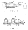
- LPE method of these methods will be described with reference to Figs. 1 and 2.
- the solutions 24, 24 are injected from the upper solution containers 23a and 23b in the holes 26a and 26b in each of which the crystalline semiconductor substrate 27 is arranged.
- a carrier gas is flowed in the quartz tube 21 at a flow rate of 0.3 to 5l/min, each semiconductor substrate 27 is held in the uniform heat region 21a which is maintained at 1,050 to 1,100°C for 60 to 90 minutes, thereby reliably performing LPE.
- the semiconductor substrate 27 is annealed to 800°C at a temperature gradient of 0.5 to 2°C/min. As the temperature falls upon annealing, a supersaturated polycrystal is formed as an LPE layer consisting of single crystals.
- the substrate holder 26 which holds the substrates 27 in the holes 26a and 26b and the containers 23a and 23b which contain the predetermined solutions 24, 24 respectively are arranged in the uniform heat region 21a of the quartz tube 21. Heating and annealing are then performed in accordance with a predetermined temperature gradient.
- the substrate 27, i.e., a Gap or GaAs substrate to be subjected to LPE is in contact with a carrier gas until predetermined amount of the solutions are injected. Therefore, phosphorus (P) or arsenic (As) is released from the GaP, GaAs or GaAlAs substrate, i.e., so-called gas etching occurs to adversely affect the LPE layer to be grown thereafter. That is, in a light-emitting device or a laser device, a poly-element compound consisting of a Group III-V semiconductor compound is used and a compound of elements in amounts of fractions in terms of a stoichiometric ratio is used. Therefore, a stoichiometric ratio essential to an LPE film consisting of a Group III-V semiconductor compound is adversely affected to disable predetermined characteristics to be achieved.
- the present invention has been made in consideration of the above situation and has as its object to provide an LPE method which can form an LPE film which is not adversely affected by gas etching on a crystalline semiconductor substrate and an apparatus therefor.
- a crystalline semiconductor substrates are sealed between a substrate holder and an upper solution container member which oppose each other, and are heated from room temperature to a high temperature.
- a predetermined amount of a solution mixture consisting of a Group III-V compound semiconductor and a dopant is added to the crystalline semiconductor substrate which is then annealed, thereby forming an LPE layer on the crystalline semiconductor substrate.
- a bottom blocking member is additionally provided to a double-layered structure which is constituted by the upper solution container member and the substrate holder, so that the heating step and the LPE step in the sealed condition can be performed respectively in different places.
- the heating step openings of through holes formed in the substrate holder to receive the crystalline semiconductor substrates are closed by the upper solution containing member and the bottom blocking member to obtain the sealed condition and then the substrates are heated.
- the crystalline semiconductor substrate is moved into a hole formed in the bottom blocking member, and a solution mixture of a polycrystalline solution of a Group III-V compound semiconductor and a dopant solution formed in solution containers of an upper solution container member in the heating step is injected through an empty through hole, thereby forming an LPE layer having a predetermined thickness.
- All of the upper solution container member, the substrate holder and the bottom blocking member are formed of a conductive material, e.g., carbon to be maintained at the same temperature in the heating step.
- the upper solution container member, the substrate holder and the bottom blocking member are allowed to move relative to each other. Normally, the substrate holder is fixed while the upper solution container member and the bottom blocking member are moved.
- a crystalline semiconductor substrate of 300 to 500 ⁇ m thickness is fixed on a storage jig for crystalline semiconductor substrate and placed in a through hole of 0.5 mm depth, thereby substantially eliminating a clearance between the semiconductor substrate and the upper solution containing member.
- This storage jig also serves as a protecting member during movement of the crystalline semiconductor substrate consisting of a hard and brittle Group III-V compound semiconductor such as GaAs into the hole in the bottom blocking member.
- an LPE layer having a predetermined thickness can be formed.
- an LPE layer having a predetermined thickness and a predetermined composition can be formed.
- Figs. 4A, 4B, 4C and 4D are sectional views schematically showing micrographs of formed LPE layer, in which Figs. 4A and 4B show LPE layer obtained by the present invention and Figs. 4C and 4D show those obtained by conventional methods.
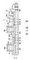
- An LPE method and an apparatus therefor according to the present invention will be described in detail below with reference to Fig. 3 and Figs. 4A to 4D. A part of the descriptions will be made with reference to Fig. 1.
- An upper solution containing member 2, a substrate holder 3 and a bottom blocking member 4 are vertically arranged in a quartz tube 21 serving as a reaction tube of an LPE apparatus 1, thereby constituting the LPE apparatus 1 shown in Fig. 3.
- the upper solution containing member 2, the substrate holder 3 and the bottom blocking member 4 consist of a conductive material.
- a uniform heat region 21a in the quartz tube 21 is maintained at a predetermined temperature with heating the quartz tube 21 by a heating unit 22, a carrier gas such as Ar is flowed at a predetermined rate of 0.3 to 5l/min.
- a carrier gas such as Ar
- solution mixtures 6 and 6 consisting of a Group III-V compound semiconductor polycrystal and a dopant are arranged in upper solution containers 2a and 2b.
- the present invention is characterized in that the bottom blocking member 4 is arranged below the substrate holder 3 so that the surface of a crystalline semiconductor substrate 10 consisting of a Group III-V compound semiconductor is kept in contact with the bottom surface of the substrate holder 3 and then the substrate is heated to form an LPE layer.
- Upper solution containers 2a and 2b for containing the solution mixtures 6 and 6 consisting of a polycrystal of a Group III-V compound semiconductor such as GaP, GaAs or the like and the dopant, respectively, are formed in the upper solution containing member 2.
- Cover members 8a and 8b are formed on the containers 2a and 2b, respectively, thereby preventing evaporation of the Group III-V compound semiconductor polycrystal having a high vapor pressure.
- a hole 2c is formed in a bottom plate 2d so that a bent portion 13a at the distal end of a manipulating rod 13 is fitted therein.
- Through holes 3a and 3a are formed in the substrate holder 3 at positions corresponding to the bottom plates 2d and 2d of the upper solution containing member 2.
- a crystalline semiconductor substrates 10 of 250 to 300- ⁇ m thickness is placed in each through hole 3a as will be described later.
- the bottom plate 2d of the upper solution containing member 2 and the upper surface of the bottom blocking member 4 located below the through holes 3a cover the upper and lower openings of each through hole 3a, thereby sealing the through hole 3a.
- the crystalline semiconductor substrate 10 is fixed in an upper recess portion 12a of a substrate storage jig 12 and the storage jig 12 is placed in the through hole 3a so that the substrate 10 is substantially brought into contact with the bottom plate 2d of the upper solution containing member 2 covering the opening of the through hole 3a. Therefore, the depth of the through hole 3a is adjusted in accordance with the thicknesses of the substrate 10 and the jig 12 as needed.
- the substrate storage jig 12 also serves as a protecting member used when the Group III-V compound semiconductor consisting of hard and brittle GaAs, Gap and the like is moved from the through hole 3a to a hole 4a formed in the bottom blocking member 4.
- a through hole 4b for receiving a bent portion at the distal end of a manipulating rod 5 is formed in the end portion of the bottom blocking member 4.
- the sealed condition described above is obtained by moving the bottom blocking member 4 with respect to the substrate holder 3 to a predetermined position as shown in Fig. 3.
- the bottom blocking member 4 is moved while the substrate holder 3 is fixed.
- the present invention is not limited to this embodiment. For example, while the bottom blocking member 4 is fixed, the substrate holder 3 and the upper solution containing member 2 may be moved. That is, the LPE apparatus 1 need only be arranged such that these members can move relative to each other.
- An inert gas such as Ar or a reduction gas such as hydrogen gas is filled in or flowed through the quartz tube 21 in which the crystalline semiconductor substrate 10 is sealed.
- the quartz tube 21 is then heated from room temperature to 900 to 1,100°C and held at this temperature for 20 to 120 minutes, thereby forming solution mixtures 6 and 6 consisting of the Group III-V compound semiconductor polycrystal and the dopant in the upper solution containers 2a and 2b, respectively.
- a solution mixture of gallium, GaAs polycrystal, aluminum and dopant is heated to melt and homogeneously diffuse the other additives, i.e., the GaAs polycrystal, aluminum and the dopant in gallium.
- the bottom blocking member 4 is moved by the above manipulation using the manipulating rod 5 so that the through holes 3a and 3a of the substrate holder 3 coincide with the holes 4a and 4a of the bottom blocking member 4, thereby dropping the crystalline semiconductor substrates 10 in the substrate storage jigs 12 into the holes 4a and 4a.
- the upper solution containing member 2 is moved by the manipulating rod 13 to inject predetermined amount of the solution mixtures 6 and 6 on the surface of each semiconductor substrate 10 exposed in the hole 4a.
- the LPE apparatus 1 is annealed at a rate of 0.3 to 2.0°C/min to form an LPE layer on the surface of the semiconductor substrate 10. Upon this annealing, since a predetermined space is formed above the semiconductor substrate 10 placed in a space formed by facing the hole 4a and the through hole 3a, an LPE layer having a predetermined thickness can be formed on the semiconductor substrate 10.
- Figs. 4A to 4D are sectional views schematically showing micrographs of LPE layers formed by such an LPE method.
- the section of the LPE layer is not damaged by gas etching but smooth. That is, even if arsenic or phosphorus is more or less released from the LPE layer, the formed cavity has a length of less than 5 ⁇ m and a depth of 5 ⁇ m at the central portion of the LPE layer (Fig. 4A) and a length of less than 50 ⁇ m and a depth of 20 ⁇ m at its peripheral portion (Fig. 4B).
- a large number of linear or curved cavities from which arsenic or phosphorus is removed are found on LPE layers formed by the conventional techniques. That is, as shown in Figs. 4C and 4D, a cavity having a length of 20 to 100 ⁇ m and a depth of 100 ⁇ m is formed at the central portion of the LPE layer (Fig. 4C) and that having a length of 100 to 300 ⁇ m and a depth of 150 ⁇ m is formed at its peripheral portion (Fig. 4D).
- the LPE layer according to the present invention has a perfectly smooth surface and is subjected to almost no damage by gas etching as compared with those obtained by the conventional techniques. Therefore, a light-emitting element or a semiconductor laser element using the LPE layer according to the present invention can satisfactorily achieve predetermined characteristics.
Landscapes
- Chemical & Material Sciences (AREA)
- Engineering & Computer Science (AREA)
- Crystallography & Structural Chemistry (AREA)
- Materials Engineering (AREA)
- Metallurgy (AREA)
- Organic Chemistry (AREA)
- Inorganic Chemistry (AREA)
- Liquid Deposition Of Substances Of Which Semiconductor Devices Are Composed (AREA)
- Crystals, And After-Treatments Of Crystals (AREA)
Applications Claiming Priority (2)
| Application Number | Priority Date | Filing Date | Title |
|---|---|---|---|
| JP111611/89 | 1989-04-28 | ||
| JP1111611A JPH02291116A (ja) | 1989-04-28 | 1989-04-28 | 液層エピタキシャル成長方法 |
Publications (2)
| Publication Number | Publication Date |
|---|---|
| EP0394826A2 true EP0394826A2 (fr) | 1990-10-31 |
| EP0394826A3 EP0394826A3 (fr) | 1992-03-11 |
Family
ID=14565726
Family Applications (1)
| Application Number | Title | Priority Date | Filing Date |
|---|---|---|---|
| EP19900107368 Withdrawn EP0394826A3 (fr) | 1989-04-28 | 1990-04-18 | Méthode de croissance épitaxiale de cristaux en phase liquide et appareil à cet effet |
Country Status (3)
| Country | Link |
|---|---|
| EP (1) | EP0394826A3 (fr) |
| JP (1) | JPH02291116A (fr) |
| KR (1) | KR900017109A (fr) |
Family Cites Families (5)
| Publication number | Priority date | Publication date | Assignee | Title |
|---|---|---|---|---|
| US3925117A (en) * | 1971-05-28 | 1975-12-09 | Texas Instruments Inc | Method for the two-stage epitaxial growth of iii' v semiconductor compounds |
| NL185375C (nl) * | 1980-01-16 | 1990-03-16 | Philips Nv | Inrichting voor het epitaxiaal aanbrengen van een laag halfgeleidermateriaal. |
| JPS56111214A (en) * | 1980-02-07 | 1981-09-02 | Nippon Telegr & Teleph Corp <Ntt> | Carbon slider boat apparatus for liquid phase epitaxial growth |
| US4470368A (en) * | 1982-03-10 | 1984-09-11 | At&T Bell Laboratories | LPE Apparatus with improved thermal geometry |
| GB2138697A (en) * | 1983-04-27 | 1984-10-31 | Philips Electronic Associated | Liquid phase epitaxy apparatus |
-
1989
- 1989-04-28 JP JP1111611A patent/JPH02291116A/ja active Pending
-
1990
- 1990-04-18 EP EP19900107368 patent/EP0394826A3/fr not_active Withdrawn
- 1990-04-28 KR KR1019900006030A patent/KR900017109A/ko not_active Abandoned
Also Published As
| Publication number | Publication date |
|---|---|
| JPH02291116A (ja) | 1990-11-30 |
| EP0394826A3 (fr) | 1992-03-11 |
| KR900017109A (ko) | 1990-11-15 |
Similar Documents
| Publication | Publication Date | Title |
|---|---|---|
| US3974002A (en) | MBE growth: gettering contaminants and fabricating heterostructure junction lasers | |
| US3839084A (en) | Molecular beam epitaxy method for fabricating magnesium doped thin films of group iii(a)-v(a) compounds | |
| US3715245A (en) | Selective liquid phase epitaxial growth process | |
| US3909317A (en) | Formation of abrupt junctions in liquid phase epitaxy | |
| US4308820A (en) | Apparatus for epitaxial crystal growth from the liquid phase | |
| US4030949A (en) | Method of effecting liquid phase epitaxial growth of group III-V semiconductors | |
| US3549401A (en) | Method of making electroluminescent gallium phosphide diodes | |
| US4482423A (en) | Protection of semiconductor substrates during epitaxial growth processes | |
| US3762968A (en) | Method of forming region of a desired conductivity type in the surface of a semiconductor body | |
| US4227962A (en) | Prevention of decomposition of phosphorous containing substrates during an epitaxial growth sequence | |
| EP0394826A2 (fr) | Méthode de croissance épitaxiale de cristaux en phase liquide et appareil à cet effet | |
| US3810794A (en) | Preparation of gap-si heterojunction by liquid phase epitaxy | |
| US3925117A (en) | Method for the two-stage epitaxial growth of iii' v semiconductor compounds | |
| US3891478A (en) | Deposition of epitaxial layer from the liquid phase | |
| JP2599767B2 (ja) | 溶液成長装置 | |
| CA1204526A (fr) | Methode d'epitaxie a partir d'une phase liquide | |
| Dawson | Liquid phase epitaxy (LPE) techniques for compound semiconductor growth | |
| van Oirschot et al. | LPE growth of DH laser structures with the double source method | |
| JP4870859B2 (ja) | 液相エピタキシャル成長装置及び成長方法 | |
| JPH0419196B2 (fr) | ||
| Lozovskii et al. | Isothermal liquid phase epitaxy | |
| JP2823760B2 (ja) | 液相エピタキシャル成長装置 | |
| JPH027464Y2 (fr) | ||
| JPS62202893A (ja) | 液相エピタキシヤル成長方法 | |
| JP2975740B2 (ja) | 液相エピタキシャル成長方法 |
Legal Events
| Date | Code | Title | Description |
|---|---|---|---|
| PUAI | Public reference made under article 153(3) epc to a published international application that has entered the european phase |
Free format text: ORIGINAL CODE: 0009012 |
|
| 17P | Request for examination filed |
Effective date: 19900419 |
|
| AK | Designated contracting states |
Kind code of ref document: A2 Designated state(s): DE FR GB |
|
| RAP1 | Party data changed (applicant data changed or rights of an application transferred) |
Owner name: KABUSHIKI KAISHA TOSHIBA |
|
| PUAL | Search report despatched |
Free format text: ORIGINAL CODE: 0009013 |
|
| AK | Designated contracting states |
Kind code of ref document: A3 Designated state(s): DE FR GB |
|
| STAA | Information on the status of an ep patent application or granted ep patent |
Free format text: STATUS: THE APPLICATION HAS BEEN WITHDRAWN |
|
| 18W | Application withdrawn |
Withdrawal date: 19930908 |