EP0395231A2 - Schutzanordnung für eine Leitungsschnittstellenschaltung einer Fernmeldeanlage - Google Patents
Schutzanordnung für eine Leitungsschnittstellenschaltung einer Fernmeldeanlage Download PDFInfo
- Publication number
- EP0395231A2 EP0395231A2 EP90303518A EP90303518A EP0395231A2 EP 0395231 A2 EP0395231 A2 EP 0395231A2 EP 90303518 A EP90303518 A EP 90303518A EP 90303518 A EP90303518 A EP 90303518A EP 0395231 A2 EP0395231 A2 EP 0395231A2
- Authority
- EP
- European Patent Office
- Prior art keywords
- substrate
- circuit
- fracturing
- fuse
- fuse conductor
- Prior art date
- Legal status (The legal status is an assumption and is not a legal conclusion. Google has not performed a legal analysis and makes no representation as to the accuracy of the status listed.)
- Granted
Links
Images


Classifications
-
- H—ELECTRICITY
- H01—ELECTRIC ELEMENTS
- H01T—SPARK GAPS; OVERVOLTAGE ARRESTERS USING SPARK GAPS; SPARKING PLUGS; CORONA DEVICES; GENERATING IONS TO BE INTRODUCED INTO NON-ENCLOSED GASES
- H01T4/00—Overvoltage arresters using spark gaps
-
- H—ELECTRICITY
- H04—ELECTRIC COMMUNICATION TECHNIQUE
- H04M—TELEPHONIC COMMUNICATION
- H04M3/00—Automatic or semi-automatic exchanges
- H04M3/18—Automatic or semi-automatic exchanges with means for reducing interference or noise; with means for reducing effects due to line faults with means for protecting lines
-
- H—ELECTRICITY
- H01—ELECTRIC ELEMENTS
- H01H—ELECTRIC SWITCHES; RELAYS; SELECTORS; EMERGENCY PROTECTIVE DEVICES
- H01H85/00—Protective devices in which the current flows through a part of fusible material and this current is interrupted by displacement of the fusible material when this current becomes excessive
- H01H85/02—Details
- H01H85/04—Fuses, i.e. expendable parts of the protective device, e.g. cartridges
- H01H85/041—Fuses, i.e. expendable parts of the protective device, e.g. cartridges characterised by the type
- H01H85/046—Fuses formed as printed circuits
-
- H—ELECTRICITY
- H01—ELECTRIC ELEMENTS
- H01H—ELECTRIC SWITCHES; RELAYS; SELECTORS; EMERGENCY PROTECTIVE DEVICES
- H01H85/00—Protective devices in which the current flows through a part of fusible material and this current is interrupted by displacement of the fusible material when this current becomes excessive
- H01H85/02—Details
- H01H85/04—Fuses, i.e. expendable parts of the protective device, e.g. cartridges
- H01H85/041—Fuses, i.e. expendable parts of the protective device, e.g. cartridges characterised by the type
- H01H85/048—Fuse resistors
-
- H—ELECTRICITY
- H01—ELECTRIC ELEMENTS
- H01H—ELECTRIC SWITCHES; RELAYS; SELECTORS; EMERGENCY PROTECTIVE DEVICES
- H01H85/00—Protective devices in which the current flows through a part of fusible material and this current is interrupted by displacement of the fusible material when this current becomes excessive
- H01H85/0039—Means for influencing the rupture process of the fusible element
- H01H85/0073—Expansion or rupture of the insulating support for the fusible element
-
- H—ELECTRICITY
- H05—ELECTRIC TECHNIQUES NOT OTHERWISE PROVIDED FOR
- H05K—PRINTED CIRCUITS; CASINGS OR CONSTRUCTIONAL DETAILS OF ELECTRIC APPARATUS; MANUFACTURE OF ASSEMBLAGES OF ELECTRICAL COMPONENTS
- H05K1/00—Printed circuits
- H05K1/02—Details
- H05K1/0286—Programmable, customizable or modifiable circuits
- H05K1/0293—Individual printed conductors which are adapted for modification, e.g. fusable or breakable conductors, printed switches
-
- H—ELECTRICITY
- H05—ELECTRIC TECHNIQUES NOT OTHERWISE PROVIDED FOR
- H05K—PRINTED CIRCUITS; CASINGS OR CONSTRUCTIONAL DETAILS OF ELECTRIC APPARATUS; MANUFACTURE OF ASSEMBLAGES OF ELECTRICAL COMPONENTS
- H05K1/00—Printed circuits
- H05K1/02—Details
- H05K1/03—Use of materials for the substrate
- H05K1/0306—Inorganic insulating substrates, e.g. ceramic, glass
-
- H—ELECTRICITY
- H05—ELECTRIC TECHNIQUES NOT OTHERWISE PROVIDED FOR
- H05K—PRINTED CIRCUITS; CASINGS OR CONSTRUCTIONAL DETAILS OF ELECTRIC APPARATUS; MANUFACTURE OF ASSEMBLAGES OF ELECTRICAL COMPONENTS
- H05K1/00—Printed circuits
- H05K1/16—Printed circuits incorporating printed electric components, e.g. printed resistors, capacitors or inductors
- H05K1/167—Printed circuits incorporating printed electric components, e.g. printed resistors, capacitors or inductors incorporating printed resistors
Definitions
- This invention relates to a means of protecting a telecommunications subscriber line interface circuit from high voltages, and also relates to a novel fuse device or circuit protection device for the protection of a wide range of circuits, including solid-state circuitry.
- SLIC subscriber line interface circuits
- solid state components utilizing for example Zener diodes, SCR crowbar, MOV or diodes, can be coupled between each conductor of the telephone line to ground.
- a small resistance can be inserted into each line, such as about 100 ohms, to limit the maximum surge current to a finite value. Since it is typical for the current limiting resistors to be inserted in series with the telephone line conductors, it is necessary that the resistances be equal to within a fraction of an ohm in order not to adversely affect the longitudinal balance of the telephone line interface.
- the novel circuit protection device in accordance with this invention may principally comprise a thick film resistor and a mechanically coupled fuse conductor, which opens when the resistor fails open.
- Thick film resistors typically fail due to the application of excessive power by breaking in half, that is, the substrate on which the thick film is printed cracks in half, resulting in both an electrical and physical (mechanical) open circuit.
- the present invention takes advantage of the expected failure mode of the typical thick film resistor.
- the cracking of the substrate is due to the unequal thermal expansion of the two surfaces of the substrate.
- heat is generated only on one side of the frangible substrate, the side where the resistor is located, so the thermal expansion is greater on that side, when compared with the other.
- the temperature differential between the two surfaces of the substrate causes a mechanical stress that is focused at the middle of the substrate.
- the total mechanical stress in the substrate is the direct result of two orthogonally related temperature differentials, primarily the surface to surface differential, and secondly the top to bottom differential, which results in the focussing of the mechanical stress at a location in the upper middle portion of the substrate.
- the fuse conductor provided on the substrate may be critical to the success of the instant device. Thus, it is important for the fuse conductor to be disposed at the location that represents the focus of the mechanical stress, which is across the top of the single in line package. At this location of the focus of the orthogonally related mechanical stresses, the cracking or fracturing of the substrate begins at the time of a predetermined level of overcurrent through the resistor.
- the fuse conductor it is most important for the proper operation of my invention for the fuse conductor to be severed completely before the resistor opens, because it is the heat being generated in the resistor that is the source of the enabling mechanical stress. If the resistor should open before the novel fuse conductor is severed, the mechanical stress could be removed before the fuse conductor breaks, resulting in a device that is no more effective in protecting sensitive devices than the basic resistor acting alone would have been.
- an aspect of this device is the placement of the fuse conductor wire across the top of the device, where it is sure to be broken by the two orthogonally related cambering effects, due to the heating of the resistor.
- This conductor wire is placed in series with the feedback sense or high impedance input of an adjacent solid state SLIC.
- the fuse conductor is, fortuitously, also severed, due to the novel mechanical coupling present between the resistor and fuse conductor. Therefore, quite advantageously, both the low and high impedance inputs to the solid state SLIC are electrically and physically isolated from the high voltage potential, thus quite effectively protecting the expensive SLIC.
- one substantial advantage of this device is that all the exposed inputs of the SLIC are isolated both electrically and physically from the foreign potential when the resistor fails. Because the resistor portion of my device fails before any damage occurs to the SLIC, it is to be seen that a relatively inexpensive part or component can be readily replaced by the user, thus restoring the Line Interface Circuit to an operational condition without necessitating that it be sent back to the manufacturer.
- this circuit protection device could be constructed utilizing thin film resistor technology, although the thin film implementation would be slightly more expensive. Also, the fuse conductor could be connected in series with the telephone line conductors and disconnect the SLIC from the foreign potential in that manner. The conductor would then have to be made with relatively expensive materials or solder dipped in order to minimize the magnitude of its resistance, so longitudinal balance would not be adversely affected.
- Heat induced mechanical stress is the primary failure mode or mechanism of my novel device.
- the resistor substrate can be made smaller and handle the same power if the resistor is printed on both sides of the substrate, but in this instance the ohmage values of the two resistors must be different.
- the temperature differential between the two surfaces of the substrate is reduced, hence, the thermal expansion of the substrate surfaces is equal and less "bending" (mechanical stress) occurs. Since the cracking is a desired effect and a small, inexpensive resistor is also desired, it is feasible to utilize unequal resistors, one on each side, resulting in a smaller resistor with a designed thermal differential (mechanical stress) which predictably fails by cracking or fracturing into two or more pieces.
- the invention is not limited to the use of a single fuse conductor, for in various multi-circuit applications of my invention it may be highly desirable to use a plurality of electrically separate fuse conductors.
- the device 10 utilizes a substrate 12, which is a substantially flat member of non-conductive, frangible material, such as alumina substrate.
- the substrate 12 is of generally rectangular configuration, and it is to be realized that the substrate is relatively thin, being for example .040 inches thick, with opposed parallel flat surfaces.
- the preferred substrate material has the nominal characteristic of more than 90% alumina and has a thermal capacity of approximately Quite obviously I am to be limited to neither this material nor to this particular thickness.
- one critical aspect of my circuit protection device is that the lower edge 16 of the frangible substrate be fixed with respect to a circuit board 30 or the like upon which it is mounted, so as to assure proper operation of my device in the event of an overload condition.
- connection pins 20, 22 and 24 are disposed in a straight array along the first or lower edge 16 of the substrate, so as to enter holes in the circuit board 30 that are precisely placed along a straight line.
- the lower edge 16 may be spaced .030 inches to .040 inches off the circuit board 30 to prevent scorching of the circuit board should an overcurrent condition through the resistive component on the substrate be encountered.
- Figure 1 reveals that the second, opposite edge 18 of the relatively fragile substrate remains free, and in the illustrated instance, this free edge is at the top of the substrate 12.
- a resistive element 26 is tightly affixed on one flat surface of the frangible substrate 12, applied such as by a standard thick film (or thin film) resistor process.
- the resistance material can be screened onto the substrate at room temperature, and the substrate later baked to cause the resistance material to harden properly.
- the application of resistive material to the frangible substrate entails several distinct stages, involving for example the steps of cleaning, screening, drying, then baking the substrate.
- the resistive material may for example be made up of a carbon-metal nux.
- the resistive element 26 extends widthwise across a substantial portion of the one flat surface of the substrate, and is disposed generally parallel to the first edge 16, along which the connection pins are located. It is to be understood that the resistive element 26 is electrically connected by the connection pins 20 and 22 to a first portion of the associated electrical circuit.
- a fuse conductor 28 is also tightly affixed on the one flat surface of the substrate 12, at a location spaced just above the resistor 26 as viewed in Figure 1.
- the fuse conductor may for example be a strip of palladium silver, an aluminium strip, or the like. I may choose to refer to the fuse conductor 28 in some instances as a "fuse strip", a "fusible conductor", or a "conductor wire”.
- the fuse conductor 28 is located generally adjacent the resistive element 26, but disposed near the second or upper edge 18 of the substrate 12. It is to be noted that the fuse conductor 28 is electrically connected to a second portion of the associated electrical circuit 44 by means of two of the previously mentioned connection pins, these being pins 20 and 24.
- my invention may be created by either thick film or thin film techniques, with thick film of course being less expensive, and thin film representing high performing technology. In either event, the result is the same when the substrate cracks and fractures, namely, both the resistive component and the fuse conductor break, thus preventing damage to the associated circuits. It is typical to utilize either thin film techniques or thick film techniques, but not to use these techniques in an intermixed relationship.
- the fuse conductor and the resistive element may be created at the same time. This is possible if, for example, their ohmage values are in the same range, such as the fuse conductor having eight ohms resistance, and the resistive element being a twenty ohm resistor. Creating these components at the same time becomes less likely when the ohmage values are quite different, such as when an eight ohm fuse conductor is utilized with a one hundred ohm resistance element.
- Figure 2a it will be noted from this somewhat idealized, no-scale showing, that this figure depicts the resistor 26 and the substrate 12 in their normal or unstressed condition.
- the resistor When the resistor is carrying a normal amount of current, it remains flat, but when carrying an overcurrent, the resistor tends to heat and elongate.
- Figure 2b is a figure drawn specifically with the goal in mind of depicting the primary mechanical stress that becomes involved in the practice of this invention at the time of an overcurrent through the resistor.
- the dimension L shown on the side of substrate 12 opposite the resistor 26 in Figure 2b represents the basic or original length of the substrate, whereas the dimension L+DL depicts the length of the substrate as a result of the thermal expansion of the near surface of the substrate due to the overcurrent through the resistor 26.
- T near the bottom of substrate 12 in Figure 2b represents the reference temperature
- T+DT near the top of the substrate represents the increase in temperature of the surface of the substrate due to overcurrent through the resistor.
- the resistor material and the substrate tend to undertake the curved configuration depicted in Figure 2b at the time of an overcurrent through the resistor.
- the substrate material to some extent resists this expansion and bending of the resistor material, but inasmuch as the substrate is rather fragile and entirely unable to withstand a considerable amount of bending, the unequal heating of the two faces of the substrate causes a vertical crack 32 to form in the substrate material, that is, to form in a direction perpendicular to the circuit board 30. This crack is thus formed as a result of the primary mechanical stress involved in my invention.
- Certain embodiments of my invention are designed to fail at the time of an overcurrent, as a result of this primary failure mode. These embodiments of my invention could be effectively used when alternative means of mechanical interconnection are used to secure the substrate to the circuit board, and the substrate is not installed in an essentially perpendicular relationship to the circuit board by the use of pins arrayed in a straight line.
- FIG. 2c Other embodiments of my invention may involve more than the aforementioned primary mechanical stress, for as depicted in Figure 2c, a secondary mechanical stress, orthogonal to the primary stress, is brought about in the substrate material as a result of the restraint brought about by the anchoring of the pins 20, 22 and 24 in the holes disposed along a straight line in the circuit board material 30.
- Thick film resistors fail due to excessive power by breaking in two, that is, the substrate on which they are printed cracks in half, resulting in both an electrical and a physical (mechanical) open circuit.
- the cracking is of course due to the unequal thermal expansion of the two surfaces of the frangible substrate. Since in this embodiment heat is only being generated on the surface of the substrate 12 on which the resistance 26 is disposed, the thermal expansion is greater on one substrate surface than the other.
- the temperature differential between the two surfaces of the substrate causes a mechanical stress focussed at the middle of the substrate, as previously mentioned, leading to a fracturing of the substrate and the electrical components thereon.
- the terminal pins 20, 22 and 24 are soldered into the printed circuit board 30 in a straight line. These input/output pins physically hold the bottom edge 16 of the substrate 12 in a straight line just above the circuit board, and act as a heat sink on the bottom of the substrate.
- the spacing can be .030 inches to .040 inches from the circuit board. This causes a temperature differential to exist between the top and the bottom of the component, focussing the mechanical stress quite near the top of the device, as indicated in Figure 2c.
- the proper placement of the fuse conductor strip 28 on the substrate is critical to the success of my device.
- the fuse conductor is placed across the top of the substrate because in the embodiment depicted in the first several figures of drawing, this location is the focus of the heat induced mechanical stress. It is at the focus of the mechanical stress where the cracking or fracturing of the substrate begins.
- the fuse conductor 28 must be severed completely before the resistor 26 opens due to the cracking of the substrate 12, because it is the heat generated in the resistor that is the basic source of the above-described mechanical stress.
- the resistor 26 should open before the fuse conductor 28 is severed as a result of the stress fractures in substrate 12, the mechanical stress could be removed before the conductor 28 is severed, and that would of course result in a device no more effective than a resistor acting alone. It may therefore be seen that my above-described novel arrangement is somewhat analogous to the opening of a current limiting resistor.
- a device in accordance with this invention may involve a frangible substrate having thereon a plurality of electrically separate fuse conductors.
- one of such fuse conductors can continue to share a pin in common with the resistor designed to bring about the cracking of the substrate when an undesirable high overcurrent condition has occurred in the low impedance circuit.
- fuse conductors are on one side of the substrate, for quite obviously at least one fuse conductor can be effectively utilized on each side of the substrate, as long as such fuse conductors are disposed in a location corresponding to position 34 revealed in Figure 2d, where cracking is concentrated.
- Figure 4 I reveal an embodiment in which a resistive element is utilized on both sides of the frangible substrate, with such elements being in an electrically parallel relationship.
- resistive element 36 is disposed in a location essentially opposite the resistive element 26.
- a double-sided embodiment can be physically smaller yet handle the same overload condition as the single-sided counterpart. This smaller size is possible because the primary mechanical stress due to surface-to-surface temperature differences has been reduced by heating both surfaces of the substrate simultaneously.
- resistors utilized in the double-sided embodiment are disposed in an electrically parallel relationship, such as depicted in Figure 4.
- I can use either one or multiple fuse conductors because it is within the scope of my invention to break one or more high impedance circuits when excessive current flows in the low impedance circuit of which the parallel resistors are a part.
- a fuse conductor 48 could be utilized relatively close to the resistive element 36, with the fuse conductor 48 being in approximately the same corresponding location on the one side of the substrate, as the location in which the fuse conductor 28 is utilized on the other side of the substrate 12.
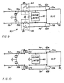
- FIG. 5 is a block diagram showing a typical utilization of my novel circuit protection device 10 with components to be found in a typical usage.
- the pin 22, attached to the resistive element is connected to the low impedance circuit
- the pin 24, connected to the fuse conductor is connected to the high impedance circuit.
- FIG. 6 I there show a known arrangement for protecting a subscriber line interface circuit 52 comprising solid state components from abnormally high voltages existing on the tip conductor 54 and the ring conductor 56 of a subscriber line.
- a solid state voltage limiting device 60 e.g. Zener diodes, SCR crowbar, MOV or diodes
- a small resistance 26a is inserted into line 54, and a small resistance 26b is inserted into line 56.
- Each of those resistors typically have a resistance value of approximately 100 ohms, to limit the maximum surge current to a finite value. Since the resistances 26a and 26b are inserted into lines 54 and 56, it is necessary that the resistances be equal to within a fraction of an ohm in order not to adversely affect the balance of the telephone line interface.
- the presence of the feedback loops 74 and 76 creates another problem in that in the event of a surge, such as for example caused by a lightening strike or AC power cross, the power flowing in the lines 54 and 56 may exceed the power rating of the resistances 26a and 26b, causing the resistances to fuse and form electrical open circuits. In the fused condition, however, there may still be a physical link across the resistances, which may not have sufficient dielectric strength to isolate inputs 62a and 62b of SLIC 52 from the surge voltage.
- the inputs 62a and 62b are normally of a low impedance.
- connections 72a and 72b of feedback loops 74 and 76 to SLIC 52 which normally have a high impedance, are in any case exposed to the high surge voltage. This situation is indicated schematically in Figure 8, where open circuits are created by the failure of resistors 26a and 26b. The high voltage surge, experience has shown, will often damage high impedance connections 72a and 72b, whereupon replacement or repair of SLIC 52 is necessary, which is an expensive operation.
- a preferred form of my invention is seen to comprise a circuit organization 80 formed of a line interface circuit (SLIC) 52 and adjunct circuit elements 84 and 86 provided for the protection of the SLIC against damage by electrical surge or overload condition from the subscriber line.
- SLIC line interface circuit
- One rectangle formed of dashed lines is seen in Figure 9 to define circuit element 84, whereas the other rectangle formed of dashed lines in Figure 9 is seen to define the circuit element 86.
- Each of these novel circuit elements contains a resistor 26 and a fuse conductor 28.
- Circuit 80 is of the same type as earlier described, containing high-gain amplifiers which form part of negative feedback loops back around to the subscriber line side of the limiting resistors.
- the pair of carbon blocks 58a and 58b and the voltage limiter 60 have the same functions as heretofore described in connection with earlier figures.
- the first fuse and resistance unit electrical component assembly 84 is electrically connected in a circuit organization with its input side directly coupled to high impedance feedback lead 72a of SLIC circuit 52, and the lead from the limiting resistance at its output side being directly coupled to low impedance input lead 62a of circuit 52.
- the second fuse and resistance unit 86 is similarly connected between ring conductor 56 and high impedance negative feedback lead 72b and low impedance input lead 62b.
- Figure 10 reveals how, due to an overcurrent through the resistors 26 of circuit elements 84 and 86 of Figure 9, these novel circuit elements have functioned in accordance with this invention to protect the expensive SLIC against excessive voltage and current. It is likely that both of the novel fuse and resistor units will, upon the occurrence of hazardous voltages, function at approximately the same time to protect the SLIC, simultaneous functioning is not a requirement of this invention.
- one embodiment of my invention can involve configurations in which the primary stress depicted in Figure 2b to represent the unequal thermal expansion of the two surfaces of the substrate is utilized for causing a fracturing of the substrate as well as the fuse conductor.
- An example is the use of substrates created in accordance with this invention, there are to be operatively disposed in an essentially parallel relationship to the circuit board, as opposed to the essentially perpendicular relationship depicted in drawing Figure 1.
Landscapes
- Engineering & Computer Science (AREA)
- Signal Processing (AREA)
- Fuses (AREA)
- Emergency Protection Circuit Devices (AREA)
Applications Claiming Priority (2)
| Application Number | Priority Date | Filing Date | Title |
|---|---|---|---|
| GB8909354 | 1989-04-25 | ||
| GB8909354A GB2230921B (en) | 1989-04-25 | 1989-04-25 | Protective arrangement for telecommunications line interface circuit |
Publications (3)
| Publication Number | Publication Date |
|---|---|
| EP0395231A2 true EP0395231A2 (de) | 1990-10-31 |
| EP0395231A3 EP0395231A3 (de) | 1992-02-05 |
| EP0395231B1 EP0395231B1 (de) | 1995-12-20 |
Family
ID=10655650
Family Applications (1)
| Application Number | Title | Priority Date | Filing Date |
|---|---|---|---|
| EP90303518A Expired - Lifetime EP0395231B1 (de) | 1989-04-25 | 1990-04-02 | Schutzanordnung für eine Leitungsschnittstellenschaltung einer Fernmeldeanlage |
Country Status (11)
| Country | Link |
|---|---|
| EP (1) | EP0395231B1 (de) |
| JP (1) | JPH0374136A (de) |
| KR (1) | KR900017244A (de) |
| CN (1) | CN1046824A (de) |
| AU (1) | AU623513B2 (de) |
| CA (1) | CA2014086A1 (de) |
| DE (1) | DE69024252D1 (de) |
| FI (1) | FI902057A7 (de) |
| GB (1) | GB2230921B (de) |
| IE (1) | IE901451L (de) |
| PT (1) | PT93869A (de) |
Cited By (6)
| Publication number | Priority date | Publication date | Assignee | Title |
|---|---|---|---|---|
| FR2671428A1 (fr) * | 1991-01-03 | 1992-07-10 | Gould Inc | Element fusible realise a partir d'une mince pellicule de fusion deposee sur un substrat. |
| EP0507465A3 (en) * | 1991-04-02 | 1993-02-03 | Caddock Electronics, Inc. | A resistor capable of acting as a circuit breaker |
| US5361300A (en) * | 1993-01-19 | 1994-11-01 | Caddock Electronics, Inc. | Balancing resistor and thermistor network for telephone circuits, and combination thereof with relay |
| US5481242A (en) * | 1994-05-10 | 1996-01-02 | Caddock Electronics, Inc. | Debris-reducing telephone resistor combination and method |
| US5594407A (en) * | 1994-07-12 | 1997-01-14 | Caddock Electronics, Inc. | Debris-reducing film-type resistor and method |
| FR2739488A1 (fr) * | 1995-09-29 | 1997-04-04 | Navarra Componentes Electro | Element de coupe-circuit electrique avec resistance integree |
Families Citing this family (1)
| Publication number | Priority date | Publication date | Assignee | Title |
|---|---|---|---|---|
| JP2014229368A (ja) * | 2013-05-20 | 2014-12-08 | 株式会社村田製作所 | ヒューズ装置 |
Family Cites Families (4)
| Publication number | Priority date | Publication date | Assignee | Title |
|---|---|---|---|---|
| SE341746B (de) * | 1970-03-10 | 1972-09-18 | Ericsson Telefon Ab L M | |
| GB1466569A (en) * | 1973-10-05 | 1977-03-09 | Erie Electronics Ltd | Resistors |
| US4494104A (en) * | 1983-07-18 | 1985-01-15 | Northern Telecom Limited | Thermal Fuse |
| US4562509A (en) * | 1984-03-05 | 1985-12-31 | Termofrost Sweden Ab | Safety switch |
-
1989
- 1989-04-25 GB GB8909354A patent/GB2230921B/en not_active Expired - Fee Related
-
1990
- 1990-04-02 EP EP90303518A patent/EP0395231B1/de not_active Expired - Lifetime
- 1990-04-02 DE DE69024252T patent/DE69024252D1/de not_active Expired - Lifetime
- 1990-04-06 CA CA002014086A patent/CA2014086A1/en not_active Abandoned
- 1990-04-18 AU AU53689/90A patent/AU623513B2/en not_active Expired - Fee Related
- 1990-04-24 JP JP2108556A patent/JPH0374136A/ja active Pending
- 1990-04-24 IE IE901451A patent/IE901451L/xx unknown
- 1990-04-24 KR KR1019900005789A patent/KR900017244A/ko not_active Withdrawn
- 1990-04-24 FI FI902057A patent/FI902057A7/fi not_active IP Right Cessation
- 1990-04-24 PT PT93869A patent/PT93869A/pt not_active Application Discontinuation
- 1990-04-25 CN CN90103607A patent/CN1046824A/zh active Pending
Cited By (8)
| Publication number | Priority date | Publication date | Assignee | Title |
|---|---|---|---|---|
| FR2671428A1 (fr) * | 1991-01-03 | 1992-07-10 | Gould Inc | Element fusible realise a partir d'une mince pellicule de fusion deposee sur un substrat. |
| EP0507465A3 (en) * | 1991-04-02 | 1993-02-03 | Caddock Electronics, Inc. | A resistor capable of acting as a circuit breaker |
| EP0789381A1 (de) * | 1991-04-02 | 1997-08-13 | Caddock Electronics, Inc. | Widerstand, der imstande ist, als Überlastschalter zu agieren |
| US5361300A (en) * | 1993-01-19 | 1994-11-01 | Caddock Electronics, Inc. | Balancing resistor and thermistor network for telephone circuits, and combination thereof with relay |
| US5481242A (en) * | 1994-05-10 | 1996-01-02 | Caddock Electronics, Inc. | Debris-reducing telephone resistor combination and method |
| EP0682347A3 (de) * | 1994-05-10 | 1996-07-10 | Caddock Electronics Inc | Widerstand für Telefon. |
| US5594407A (en) * | 1994-07-12 | 1997-01-14 | Caddock Electronics, Inc. | Debris-reducing film-type resistor and method |
| FR2739488A1 (fr) * | 1995-09-29 | 1997-04-04 | Navarra Componentes Electro | Element de coupe-circuit electrique avec resistance integree |
Also Published As
| Publication number | Publication date |
|---|---|
| FI902057A7 (fi) | 1990-10-26 |
| JPH0374136A (ja) | 1991-03-28 |
| EP0395231B1 (de) | 1995-12-20 |
| CA2014086A1 (en) | 1990-10-25 |
| DE69024252D1 (de) | 1996-02-01 |
| FI902057A0 (fi) | 1990-04-24 |
| AU623513B2 (en) | 1992-05-14 |
| KR900017244A (ko) | 1990-11-15 |
| GB2230921B (en) | 1994-01-05 |
| GB8909354D0 (en) | 1989-06-14 |
| IE901451L (en) | 1990-10-25 |
| EP0395231A3 (de) | 1992-02-05 |
| AU5368990A (en) | 1990-11-01 |
| PT93869A (pt) | 1991-11-29 |
| CN1046824A (zh) | 1990-11-07 |
| GB2230921A (en) | 1990-10-31 |
Similar Documents
| Publication | Publication Date | Title |
|---|---|---|
| US5204799A (en) | Protective arrangement for telecommunications line interface circuit | |
| US6636409B2 (en) | Surge protection device including a thermal fuse spring, a fuse trace and a voltage clamping device | |
| US4964160A (en) | Protector device | |
| EP2008292B1 (de) | Transientenspannungsspitzenunterdrückung | |
| US5311164A (en) | Surge absorber | |
| TW201230116A (en) | Compact transient voltage surge suppression device | |
| CN107919658B (zh) | 结合有串联的热保护变阻器和放电管的部件 | |
| EP0018067A1 (de) | Leitungsschutz für einen Nachrichtenkreis | |
| EP0395231B1 (de) | Schutzanordnung für eine Leitungsschnittstellenschaltung einer Fernmeldeanlage | |
| US5254969A (en) | Resistor combination and method | |
| EP0183542A1 (de) | Stromkreisschutzanordnungen | |
| CN1132195C (zh) | 具有过载保护的混合电路装置 | |
| US20040246645A1 (en) | Telecom circuit protection apparatus | |
| EP0608077B1 (de) | Telefonschaltkreise beinhaltendes Widerstandsnetzwerk | |
| EP0507465B1 (de) | Widerstand, der imstande ist, als Überlastschalter zu agieren | |
| JP2528404B2 (ja) | 回路開放素子 | |
| JPH114535A (ja) | 保護用回路及び複合型保護用デバイス | |
| WO2002033797A1 (en) | Failsafe mechanism for telecommunications protector module | |
| CZ2002877A3 (cs) | Zařízení pro přepěťovou ochranu | |
| JPH089072A (ja) | 高電圧保護用モジュール抵抗 | |
| HK1092953B (en) | Telecom circuit protection apparatus | |
| IE84881B1 (en) | Transient voltage surge suppression | |
| JPH0817068B2 (ja) | ヒューズ抵抗器 |
Legal Events
| Date | Code | Title | Description |
|---|---|---|---|
| PUAI | Public reference made under article 153(3) epc to a published international application that has entered the european phase |
Free format text: ORIGINAL CODE: 0009012 |
|
| AK | Designated contracting states |
Kind code of ref document: A2 Designated state(s): BE DE DK ES FR GB GR IT LU NL SE |
|
| PUAL | Search report despatched |
Free format text: ORIGINAL CODE: 0009013 |
|
| AK | Designated contracting states |
Kind code of ref document: A3 Designated state(s): BE DE DK ES FR GB GR IT LU NL SE |
|
| 17P | Request for examination filed |
Effective date: 19920902 |
|
| RAP1 | Party data changed (applicant data changed or rights of an application transferred) |
Owner name: GPT LIMITED |
|
| 17Q | First examination report despatched |
Effective date: 19940429 |
|
| GRAA | (expected) grant |
Free format text: ORIGINAL CODE: 0009210 |
|
| AK | Designated contracting states |
Kind code of ref document: B1 Designated state(s): BE DE DK ES FR GB GR IT LU NL SE |
|
| PG25 | Lapsed in a contracting state [announced via postgrant information from national office to epo] |
Ref country code: IT Free format text: LAPSE BECAUSE OF FAILURE TO SUBMIT A TRANSLATION OF THE DESCRIPTION OR TO PAY THE FEE WITHIN THE PRE;WARNING: LAPSES OF ITALIAN PATENTS WITH EFFECTIVE DATE BEFORE 2007 MAY HAVE OCCURRED AT ANY TIME BEFORE 2007. THE CORRECT EFFECTIVE DATE MAY BE DIFFERENT FROM THE ONE RECORDED.SCRIBED TIME-LIMIT Effective date: 19951220 Ref country code: DK Effective date: 19951220 Ref country code: BE Effective date: 19951220 Ref country code: NL Free format text: LAPSE BECAUSE OF FAILURE TO SUBMIT A TRANSLATION OF THE DESCRIPTION OR TO PAY THE FEE WITHIN THE PRESCRIBED TIME-LIMIT Effective date: 19951220 Ref country code: FR Effective date: 19951220 Ref country code: GR Free format text: LAPSE BECAUSE OF FAILURE TO SUBMIT A TRANSLATION OF THE DESCRIPTION OR TO PAY THE FEE WITHIN THE PRESCRIBED TIME-LIMIT Effective date: 19951220 |
|
| REF | Corresponds to: |
Ref document number: 69024252 Country of ref document: DE Date of ref document: 19960201 |
|
| PG25 | Lapsed in a contracting state [announced via postgrant information from national office to epo] |
Ref country code: SE Effective date: 19960320 |
|
| PG25 | Lapsed in a contracting state [announced via postgrant information from national office to epo] |
Ref country code: DE Effective date: 19960321 |
|
| PG25 | Lapsed in a contracting state [announced via postgrant information from national office to epo] |
Ref country code: ES Free format text: LAPSE BECAUSE OF FAILURE TO SUBMIT A TRANSLATION OF THE DESCRIPTION OR TO PAY THE FEE WITHIN THE PRESCRIBED TIME-LIMIT Effective date: 19960331 |
|
| PG25 | Lapsed in a contracting state [announced via postgrant information from national office to epo] |
Ref country code: LU Free format text: LAPSE BECAUSE OF NON-PAYMENT OF DUE FEES Effective date: 19960430 |
|
| EN | Fr: translation not filed | ||
| NLV1 | Nl: lapsed or annulled due to failure to fulfill the requirements of art. 29p and 29m of the patents act | ||
| PGFP | Annual fee paid to national office [announced via postgrant information from national office to epo] |
Ref country code: ES Payment date: 19960930 Year of fee payment: 7 |
|
| PLBE | No opposition filed within time limit |
Free format text: ORIGINAL CODE: 0009261 |
|
| STAA | Information on the status of an ep patent application or granted ep patent |
Free format text: STATUS: NO OPPOSITION FILED WITHIN TIME LIMIT |
|
| 26N | No opposition filed | ||
| REG | Reference to a national code |
Ref country code: GB Ref legal event code: IF02 |
|
| PGFP | Annual fee paid to national office [announced via postgrant information from national office to epo] |
Ref country code: GB Payment date: 20020327 Year of fee payment: 13 |
|
| PG25 | Lapsed in a contracting state [announced via postgrant information from national office to epo] |
Ref country code: GB Free format text: LAPSE BECAUSE OF NON-PAYMENT OF DUE FEES Effective date: 20030402 |
|
| GBPC | Gb: european patent ceased through non-payment of renewal fee |
Effective date: 20030402 |