EP0397320A2 - Verkapselte integrierte Schaltung mit Leitergitter - Google Patents
Verkapselte integrierte Schaltung mit Leitergitter Download PDFInfo
- Publication number
- EP0397320A2 EP0397320A2 EP90303584A EP90303584A EP0397320A2 EP 0397320 A2 EP0397320 A2 EP 0397320A2 EP 90303584 A EP90303584 A EP 90303584A EP 90303584 A EP90303584 A EP 90303584A EP 0397320 A2 EP0397320 A2 EP 0397320A2
- Authority
- EP
- European Patent Office
- Prior art keywords
- leads
- dam bar
- lead frame
- severed
- integrated circuit
- Prior art date
- Legal status (The legal status is an assumption and is not a legal conclusion. Google has not performed a legal analysis and makes no representation as to the accuracy of the status listed.)
- Withdrawn
Links
Images


Classifications
-
- H—ELECTRICITY
- H10—SEMICONDUCTOR DEVICES; ELECTRIC SOLID-STATE DEVICES NOT OTHERWISE PROVIDED FOR
- H10W—GENERIC PACKAGES, INTERCONNECTIONS, CONNECTORS OR OTHER CONSTRUCTIONAL DETAILS OF DEVICES COVERED BY CLASS H10
- H10W70/00—Package substrates; Interposers; Redistribution layers [RDL]
- H10W70/40—Leadframes
- H10W70/421—Shapes or dispositions
-
- H—ELECTRICITY
- H10—SEMICONDUCTOR DEVICES; ELECTRIC SOLID-STATE DEVICES NOT OTHERWISE PROVIDED FOR
- H10W—GENERIC PACKAGES, INTERCONNECTIONS, CONNECTORS OR OTHER CONSTRUCTIONAL DETAILS OF DEVICES COVERED BY CLASS H10
- H10W70/00—Package substrates; Interposers; Redistribution layers [RDL]
- H10W70/01—Manufacture or treatment
- H10W70/04—Manufacture or treatment of leadframes
- H10W70/048—Mechanical treatments, e.g. punching, cutting, deforming or cold welding
-
- H—ELECTRICITY
- H10—SEMICONDUCTOR DEVICES; ELECTRIC SOLID-STATE DEVICES NOT OTHERWISE PROVIDED FOR
- H10W—GENERIC PACKAGES, INTERCONNECTIONS, CONNECTORS OR OTHER CONSTRUCTIONAL DETAILS OF DEVICES COVERED BY CLASS H10
- H10W72/00—Interconnections or connectors in packages
- H10W72/50—Bond wires
- H10W72/541—Dispositions of bond wires
- H10W72/5449—Dispositions of bond wires not being orthogonal to a side surface of the chip, e.g. fan-out arrangements
-
- H—ELECTRICITY
- H10—SEMICONDUCTOR DEVICES; ELECTRIC SOLID-STATE DEVICES NOT OTHERWISE PROVIDED FOR
- H10W—GENERIC PACKAGES, INTERCONNECTIONS, CONNECTORS OR OTHER CONSTRUCTIONAL DETAILS OF DEVICES COVERED BY CLASS H10
- H10W74/00—Encapsulations, e.g. protective coatings
-
- H—ELECTRICITY
- H10—SEMICONDUCTOR DEVICES; ELECTRIC SOLID-STATE DEVICES NOT OTHERWISE PROVIDED FOR
- H10W—GENERIC PACKAGES, INTERCONNECTIONS, CONNECTORS OR OTHER CONSTRUCTIONAL DETAILS OF DEVICES COVERED BY CLASS H10
- H10W90/00—Package configurations
- H10W90/701—Package configurations characterised by the relative positions of pads or connectors relative to package parts
- H10W90/751—Package configurations characterised by the relative positions of pads or connectors relative to package parts of bond wires
- H10W90/756—Package configurations characterised by the relative positions of pads or connectors relative to package parts of bond wires between a chip and a stacked lead frame, conducting package substrate or heat sink
-
- Y—GENERAL TAGGING OF NEW TECHNOLOGICAL DEVELOPMENTS; GENERAL TAGGING OF CROSS-SECTIONAL TECHNOLOGIES SPANNING OVER SEVERAL SECTIONS OF THE IPC; TECHNICAL SUBJECTS COVERED BY FORMER USPC CROSS-REFERENCE ART COLLECTIONS [XRACs] AND DIGESTS
- Y10—TECHNICAL SUBJECTS COVERED BY FORMER USPC
- Y10T—TECHNICAL SUBJECTS COVERED BY FORMER US CLASSIFICATION
- Y10T29/00—Metal working
- Y10T29/49—Method of mechanical manufacture
- Y10T29/49002—Electrical device making
- Y10T29/49117—Conductor or circuit manufacturing
- Y10T29/49121—Beam lead frame or beam lead device
Definitions
- This invention relates to the assembling and packaging of integrated circuit devices and, more particularly, to a lead frame for such devices, a method for trimming and forming an encapsulated device, and to an improved encapsulated device.
- the lead frame is placed in a mold.
- the mold is provided with a reservoir containing a quantity of insulating, molding compound.
- the molding compound is injected into the mold in order to encapsulate the integrated circuit.
- Such injection molding is accomplished as mentioned in the aforesaid patent and is further described in U.S. Patent 4,504,435, also incorporated by reference.
- each lead frame of a strip has an integrated circuit device attached to the support pad as mentioned above.
- the support pads are themselves supported by a pair of support arms between two parallel siderails.
- Each siderail is located in the plane of the lead frame and on opposite sides of the die pad.
- dual in-line package one lead frame serially follows the next.
- matrix package a plurality of lead frames are disposed between opposing siderails with transverse carrier arms disposed between the two siderails for receiving the support arms of the die pad.
- mold cavities are formed around the lead frames which tightly close and seal upon the leads themselves as well as the dam bar.
- the dam bar has a transverse portion that extends between a pair of adjoining leads.
- the dam bar restricts the flow of encapsulated material from the enclosed lead frame.
- the dam bar and a portion of the mold flashing projecting between adjoining leads is removed by a punch.
- the punch is the typical metal punch that readily severs the metallic dam bar and also removes a portion of the projected mold flashing from between the lead frames.
- the removal of the mold flashing by the dam bar punch presents several problems.
- the molding compound itself includes abrasive material such as silicon dioxide. This abrasive material wears away the cutting edge of the dies thereby reducing their useful life.
- the flashing is unevenly and jaggedly removed. As such, the portion of the flashing remaining between the leads has a jagged edge.
- Such a jagged edge mold flashing causes further problems when automatic machinery is used to insert the encapsulated integrated circuit into tightly packed printed circuit boards. The extraneous, jagged mold flashing interferes with such automatic insertion machinery thereby decreasing the efficiency and speed of the final assembly of an electronic device.
- the invention as further described and claimed herein meets the unfulfilled needs of the prior art.
- the invention provides for a dam bar disposed between each pair of adjoining leads.
- the dam bar is at least partially severed from the leads.
- the partial severance is made on that portion of the dam bar that is proximate to the molding compound.
- the dam bar is provided with lateral and transverse portions.
- the lateral portion extends between two adjoining leads and is severed from both leads and press fit back into place.
- the transverse portion is connected by its lateral portion to a support web that supports other dam bars and the leads.
- the supporting web including all of the dam bars are removed by a single punch. That punch is far removed from the molding compound and thus the life of the punch will depend substantially only upon its metal wear rather than upon the abrasive wear due to passing through molding compound.
- the invention thus provides an improved process for the assembly of an integrated circuit.
- This process includes the steps of providing a lead frame with at least one pair of adjoining leads, the lead frame having a dam bar with a transverse portion extending between the leads.
- the transverse portion of the dam bar is partially severed prior to encapsulation.
- the integrated circuit is placed on the die pad of the lead frame, and otherwise wire bonded to the leads, the integrated circuit is encapsulated with an insulating, molding compound. In this manner, the outer edge of the molding compound between the two leads is defined by the partially severed dam bar.
- the dam bar is finally removed from the leads and the leads are formed to their desired shape.
- the integrated circuit has a molded insulating material encapsulating the die.
- the outer edge of the encapsulating material disposed between adjoining leads is defined by an uncut edge. That edge conforms to the dimensions of the removed dam bar.
- Such an edge is believed unique inasmuch as the corresponding edge of all prior art devices is defined by a cutting process whereby certain portions of the mold flash between adjoining leads are removed by severing the mold compound with a metallic punch.
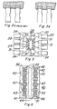
- FIG. 1 there is shown a lead frame 10 having a pair of spaced apart, parallel siderails 11, 12.
- the siderails 11, 12 are provided with a plurality of alignment apertures 13 that are used to transport and align the lead frame 10 through the use of pins or sprockets (not shown) that project through apertures 13.
- Pairs of support arms 15 extend inwardly from the siderails 11 and 12. Disposed between each pair of inwardly projecting support arms 15 is a die pad 14. The integrated circuit will be positioned on and bonded to the pad 14 at a later point in assembly.
- a plurality of leads 20 extend inwardly toward the die pad 14 from a transverse supporting web 16. Also extending from web 16 are a plurality of dam bars 25. Dam bars are disposed between the siderails 11,12 and the respective first lead 25 spaced from those siderails, as well as between adjoining pairs of leads 25.
- the dam bar 22 of the prior art is disposed between adjoining leads 20 as shown in Figure 2A and 2B.
- the dam bar 22 is spaced a sufficient distance from the ends of the leads to account for tolerance of the punch.
- a molding compound 30 is applied to the lead frame 10 and covers the end portions 21 of the leads 20.
- the trimming operation of the prior art is shown in Figure 2D.
- punches 33 and 32 respectively remove the lead web 16 as well as the dam bar 22 and a portion of the mold flash 30 that projects between adjoining leads 20.
- the double cross-hatched portion shown in Figure 22 indicates the portion of the molding compound 30 that is removed by the dam bar punch.
- the dam bar punch wears and as a result the edge of the molding compound disposed between adjoining leads assumes a ragged or jagged profile as shown in Figure 2E. Such a profile may be repeated on the corners of the molded portion of the integrated circuit. Such jagged flashings often require secondary flash removal or else they may interfere with automatic insertion equipment.
- the leads 20 have a dam bar 25 including a transverse portion 26 that is initially integral with adjoining leads 20.
- a lateral portion 27 of dam bar 25 is optional. Those skilled in the art will appreciate from the following description how the lateral portion 27 may be omitted.
- the dam bar 25, as shown in Figure 30, is partially severed along lines 23.
- the severance 23 extends preferably one-third to one-half the width of the transverse portion 26. The length of the severance is sufficient to allow a trimming punch to remove and completely sever the transverse portion 26 without passing through a molding compound.
- the molding encapsulant 30 covers the ends 21 of leads 20.
- the dam bar 26 has its severance lines 23 extending outside the molding compound 30.
- a punch 32 completes the severance of dam bar transverse portion 26.
- a further punch 33 also severs the lead web 16 together with the optional transverse portion 27 of dam bar 25.
- the resultant profile of the molding portion between two adjoining leads 20 is shown in Figure 3E. As will be seen therein, the outline of the mold portion 30 between two adjoining leads 20 is uncut and thus solely defined by the removed dam bar 25.
- FIGs 4A-4D shown a further embodiment of the invention where the dam bar 25 has the transverse portion 26 entirely severed from adjoining leads 20.
- the embodiment shows a transverse portion 26 that is entirely severed along lines 24.
- the dam bar 26 is press fitted back into place in order to form a solid dam against the subsequent mold compound.
- the mold compound 30 covers the ends 21 of adjoining leads 20 and fills the space between the adjoining leads up to the dam bar 26.
- FIG 4D The trim and form operation is shown in Figure 4D.
- a single punch 33 is used to remove the dam bar 25 and lead support web 16.
- this embodiment reduces the number of punching surfaces so that only one punch, 33, is required. So this embodiment reduces the number of punching surfaces and the single punch 33 is distantly spaced from the molding compound 30 so there is no possibility of its encountering the abrasive material of the molding compound.
- the resultant outline of the encapsulated device is shown in Figure 3E as it is substantially identical to the outline of the device made in accordance with the process discussed in Figures 3A-3D.
- FIG. 5 there is shown an integrated circuit 35 mounted on a die pad 14 and encapsulated in a molding compound 30.
- the integrated circuit 35 has a plurality of bond pads 37 that are bonded by wires 38 to corresponding lead ends 21.
- the edge of the molding compound 31 between adjoining leads ends as well as the corner edges 34 are uncut edged that are substantially defined by the dam bar that has been removed.
- the edges 31 and 34 are molded edges rather than cut or otherwise trimmed edges.
- the preferred embodiment for practicing the invention includes a matrix lead frame 40.
- the lead frame 41 includes a plurality of molded integrated circuits 42 that are disposed between opposing siderails 50 and 51. Alignment apertures 44 and siderails 50,51 are provided for sprockets that advance and align the matrix lead frame 40 through its processing steps.
- Leads 20 extend between spaced apart encapsulated integrated circuits 42.
- the dam bars including transverse sections 27 have been removed by a prior operation leaving only certain bur ends 46 on the adjoining leads. In a further operation, the leads between adjoining integrated circuits 42 will be separated along the line formed by the bur ends 46 of the dam bar 27.
- Siderails 50,51 have further ends 46 of the dam bars that have been removed during a prior operation.
- the matrix 40 includes further transverse carriers 43 extending between siderails 50,51 for supporting the edges of the integrated circuits 42. Support arms 15, now shown, extend between opposite carrier arms 43.
Landscapes
- Lead Frames For Integrated Circuits (AREA)
- Encapsulation Of And Coatings For Semiconductor Or Solid State Devices (AREA)
Applications Claiming Priority (2)
| Application Number | Priority Date | Filing Date | Title |
|---|---|---|---|
| US07/337,609 US5070039A (en) | 1989-04-13 | 1989-04-13 | Method of making an integrated circuit using a pre-served dam bar to reduce mold flash and to facilitate flash removal |
| US337609 | 2003-01-07 |
Publications (2)
| Publication Number | Publication Date |
|---|---|
| EP0397320A2 true EP0397320A2 (de) | 1990-11-14 |
| EP0397320A3 EP0397320A3 (de) | 1991-06-26 |
Family
ID=23321244
Family Applications (1)
| Application Number | Title | Priority Date | Filing Date |
|---|---|---|---|
| EP19900303584 Withdrawn EP0397320A3 (de) | 1989-04-13 | 1990-04-04 | Verkapselte integrierte Schaltung mit Leitergitter |
Country Status (3)
| Country | Link |
|---|---|
| US (1) | US5070039A (de) |
| EP (1) | EP0397320A3 (de) |
| JP (1) | JPH0362561A (de) |
Cited By (4)
| Publication number | Priority date | Publication date | Assignee | Title |
|---|---|---|---|---|
| US5147815A (en) * | 1990-05-14 | 1992-09-15 | Motorola, Inc. | Method for fabricating a multichip semiconductor device having two interdigitated leadframes |
| EP0535882A1 (de) * | 1991-09-30 | 1993-04-07 | Motorola, Inc. | Herstellungsverfahren für eine Halbleiterchippackung |
| EP0505290A3 (en) * | 1991-03-22 | 1993-06-23 | Fujitsu Ltd | Semiconductor device having improved leads, production process of the semiconductor device, and lead frame used in production process of the semiconductor device |
| WO1999052149A1 (de) * | 1998-04-06 | 1999-10-14 | Infineon Technologies Ag | Verwendung der baulichen beschaffenheit eines elektronischen bauteils als referenz bei der positionierung des bauteils |
Families Citing this family (129)
| Publication number | Priority date | Publication date | Assignee | Title |
|---|---|---|---|---|
| US5313102A (en) * | 1989-12-22 | 1994-05-17 | Texas Instruments Incorporated | Integrated circuit device having a polyimide moisture barrier coating |
| US5200364A (en) * | 1990-01-26 | 1993-04-06 | Texas Instruments Incorporated | Packaged integrated circuit with encapsulated electronic devices |
| US5343072A (en) * | 1990-08-20 | 1994-08-30 | Rohm Co., Ltd. | Method and leadframe for making electronic components |
| US5250842A (en) * | 1990-09-07 | 1993-10-05 | Nec Corporation | Semiconductor devices using tab tape |
| JPH05267555A (ja) * | 1992-03-23 | 1993-10-15 | Hitachi Ltd | 半導体装置およびその製造方法並びにそれに使用されるリードフレームおよびその製造方法 |
| NL195026C (nl) * | 1992-04-22 | 2003-06-18 | Yamaha Corporation | Werkwijze voor het bewerken van een raam van elektrische geleiders voor een halfgeleiderelement. |
| US5541447A (en) * | 1992-04-22 | 1996-07-30 | Yamaha Corporation | Lead frame |
| EP0646971B1 (de) * | 1993-09-30 | 1997-03-12 | Siemens Aktiengesellschaft | Zweipoliges SMT-Miniatur-Gehäuse für Halbleiterbauelemente und Verfahren zu dessen Herstellung |
| US5961860A (en) * | 1995-06-01 | 1999-10-05 | National University Of Singapore | Pulse laser induced removal of mold flash on integrated circuit packages |
| KR0148080B1 (ko) * | 1995-07-31 | 1998-08-01 | 김광호 | 반도체 리드프레임 제조방법 및 그를 이용한 반도체 칩 패키지 제조방법 |
| JPH09270488A (ja) * | 1996-01-29 | 1997-10-14 | Fujitsu Ltd | 半導体装置の製造方法 |
| US5929512A (en) * | 1997-03-18 | 1999-07-27 | Jacobs; Richard L. | Urethane encapsulated integrated circuits and compositions therefor |
| US7112474B1 (en) | 1998-06-24 | 2006-09-26 | Amkor Technology, Inc. | Method of making an integrated circuit package |
| US7005326B1 (en) | 1998-06-24 | 2006-02-28 | Amkor Technology, Inc. | Method of making an integrated circuit package |
| US7332375B1 (en) | 1998-06-24 | 2008-02-19 | Amkor Technology, Inc. | Method of making an integrated circuit package |
| US6893900B1 (en) | 1998-06-24 | 2005-05-17 | Amkor Technology, Inc. | Method of making an integrated circuit package |
| US7071541B1 (en) | 1998-06-24 | 2006-07-04 | Amkor Technology, Inc. | Plastic integrated circuit package and method and leadframe for making the package |
| US7030474B1 (en) | 1998-06-24 | 2006-04-18 | Amkor Technology, Inc. | Plastic integrated circuit package and method and leadframe for making the package |
| US6143981A (en) | 1998-06-24 | 2000-11-07 | Amkor Technology, Inc. | Plastic integrated circuit package and method and leadframe for making the package |
| US6448633B1 (en) * | 1998-11-20 | 2002-09-10 | Amkor Technology, Inc. | Semiconductor package and method of making using leadframe having lead locks to secure leads to encapsulant |
| KR20010037254A (ko) * | 1999-10-15 | 2001-05-07 | 마이클 디. 오브라이언 | 반도체패키지 |
| KR100403142B1 (ko) * | 1999-10-15 | 2003-10-30 | 앰코 테크놀로지 코리아 주식회사 | 반도체패키지 |
| KR100526844B1 (ko) * | 1999-10-15 | 2005-11-08 | 앰코 테크놀로지 코리아 주식회사 | 반도체패키지 및 그 제조방법 |
| KR20010037247A (ko) * | 1999-10-15 | 2001-05-07 | 마이클 디. 오브라이언 | 반도체패키지 |
| KR100379089B1 (ko) | 1999-10-15 | 2003-04-08 | 앰코 테크놀로지 코리아 주식회사 | 리드프레임 및 이를 이용한 반도체패키지 |
| US20070176287A1 (en) * | 1999-11-05 | 2007-08-02 | Crowley Sean T | Thin integrated circuit device packages for improved radio frequency performance |
| US6580159B1 (en) | 1999-11-05 | 2003-06-17 | Amkor Technology, Inc. | Integrated circuit device packages and substrates for making the packages |
| US6847103B1 (en) | 1999-11-09 | 2005-01-25 | Amkor Technology, Inc. | Semiconductor package with exposed die pad and body-locking leadframe |
| KR100421774B1 (ko) | 1999-12-16 | 2004-03-10 | 앰코 테크놀로지 코리아 주식회사 | 반도체패키지 및 그 제조 방법 |
| US6639308B1 (en) * | 1999-12-16 | 2003-10-28 | Amkor Technology, Inc. | Near chip size semiconductor package |
| KR100583494B1 (ko) * | 2000-03-25 | 2006-05-24 | 앰코 테크놀로지 코리아 주식회사 | 반도체패키지 |
| US7042068B2 (en) | 2000-04-27 | 2006-05-09 | Amkor Technology, Inc. | Leadframe and semiconductor package made using the leadframe |
| TW466720B (en) * | 2000-05-22 | 2001-12-01 | Siliconware Precision Industries Co Ltd | Semiconductor package with flash-prevention structure and manufacture method |
| KR20020058209A (ko) * | 2000-12-29 | 2002-07-12 | 마이클 디. 오브라이언 | 반도체패키지 |
| KR100731007B1 (ko) * | 2001-01-15 | 2007-06-22 | 앰코 테크놀로지 코리아 주식회사 | 적층형 반도체 패키지 |
| US6967395B1 (en) | 2001-03-20 | 2005-11-22 | Amkor Technology, Inc. | Mounting for a package containing a chip |
| US6545345B1 (en) | 2001-03-20 | 2003-04-08 | Amkor Technology, Inc. | Mounting for a package containing a chip |
| KR100369393B1 (ko) * | 2001-03-27 | 2003-02-05 | 앰코 테크놀로지 코리아 주식회사 | 리드프레임 및 이를 이용한 반도체패키지와 그 제조 방법 |
| KR100393448B1 (ko) | 2001-03-27 | 2003-08-02 | 앰코 테크놀로지 코리아 주식회사 | 반도체 패키지 및 그 제조 방법 |
| US7045883B1 (en) | 2001-04-04 | 2006-05-16 | Amkor Technology, Inc. | Thermally enhanced chip scale lead on chip semiconductor package and method of making same |
| US6597059B1 (en) | 2001-04-04 | 2003-07-22 | Amkor Technology, Inc. | Thermally enhanced chip scale lead on chip semiconductor package |
| US7064009B1 (en) | 2001-04-04 | 2006-06-20 | Amkor Technology, Inc. | Thermally enhanced chip scale lead on chip semiconductor package and method of making same |
| US7485952B1 (en) | 2001-09-19 | 2009-02-03 | Amkor Technology, Inc. | Drop resistant bumpers for fully molded memory cards |
| US6900527B1 (en) | 2001-09-19 | 2005-05-31 | Amkor Technology, Inc. | Lead-frame method and assembly for interconnecting circuits within a circuit module |
| US6630726B1 (en) | 2001-11-07 | 2003-10-07 | Amkor Technology, Inc. | Power semiconductor package with strap |
| US6818973B1 (en) | 2002-09-09 | 2004-11-16 | Amkor Technology, Inc. | Exposed lead QFP package fabricated through the use of a partial saw process |
| US6919620B1 (en) | 2002-09-17 | 2005-07-19 | Amkor Technology, Inc. | Compact flash memory card with clamshell leadframe |
| US7361533B1 (en) | 2002-11-08 | 2008-04-22 | Amkor Technology, Inc. | Stacked embedded leadframe |
| US7190062B1 (en) | 2004-06-15 | 2007-03-13 | Amkor Technology, Inc. | Embedded leadframe semiconductor package |
| US7723210B2 (en) | 2002-11-08 | 2010-05-25 | Amkor Technology, Inc. | Direct-write wafer level chip scale package |
| US6905914B1 (en) | 2002-11-08 | 2005-06-14 | Amkor Technology, Inc. | Wafer level package and fabrication method |
| US6798047B1 (en) | 2002-12-26 | 2004-09-28 | Amkor Technology, Inc. | Pre-molded leadframe |
| US6847099B1 (en) | 2003-02-05 | 2005-01-25 | Amkor Technology Inc. | Offset etched corner leads for semiconductor package |
| US6750545B1 (en) | 2003-02-28 | 2004-06-15 | Amkor Technology, Inc. | Semiconductor package capable of die stacking |
| US6927483B1 (en) | 2003-03-07 | 2005-08-09 | Amkor Technology, Inc. | Semiconductor package exhibiting efficient lead placement |
| US6794740B1 (en) | 2003-03-13 | 2004-09-21 | Amkor Technology, Inc. | Leadframe package for semiconductor devices |
| US7001799B1 (en) | 2003-03-13 | 2006-02-21 | Amkor Technology, Inc. | Method of making a leadframe for semiconductor devices |
| US7095103B1 (en) | 2003-05-01 | 2006-08-22 | Amkor Technology, Inc. | Leadframe based memory card |
| US7008825B1 (en) | 2003-05-27 | 2006-03-07 | Amkor Technology, Inc. | Leadframe strip having enhanced testability |
| US6897550B1 (en) | 2003-06-11 | 2005-05-24 | Amkor Technology, Inc. | Fully-molded leadframe stand-off feature |
| US7245007B1 (en) | 2003-09-18 | 2007-07-17 | Amkor Technology, Inc. | Exposed lead interposer leadframe package |
| US6921967B2 (en) * | 2003-09-24 | 2005-07-26 | Amkor Technology, Inc. | Reinforced die pad support structure |
| US7138707B1 (en) | 2003-10-21 | 2006-11-21 | Amkor Technology, Inc. | Semiconductor package including leads and conductive posts for providing increased functionality |
| US7144517B1 (en) | 2003-11-07 | 2006-12-05 | Amkor Technology, Inc. | Manufacturing method for leadframe and for semiconductor package using the leadframe |
| US7211879B1 (en) | 2003-11-12 | 2007-05-01 | Amkor Technology, Inc. | Semiconductor package with chamfered corners and method of manufacturing the same |
| US7109064B2 (en) * | 2003-12-08 | 2006-09-19 | Semiconductor Components Industries, L.L.C. | Method of forming a semiconductor package and leadframe therefor |
| US7057268B1 (en) | 2004-01-27 | 2006-06-06 | Amkor Technology, Inc. | Cavity case with clip/plug for use on multi-media card |
| US7091594B1 (en) | 2004-01-28 | 2006-08-15 | Amkor Technology, Inc. | Leadframe type semiconductor package having reduced inductance and its manufacturing method |
| US20080003722A1 (en) * | 2004-04-15 | 2008-01-03 | Chun David D | Transfer mold solution for molded multi-media card |
| US7202554B1 (en) | 2004-08-19 | 2007-04-10 | Amkor Technology, Inc. | Semiconductor package and its manufacturing method |
| US7217991B1 (en) | 2004-10-22 | 2007-05-15 | Amkor Technology, Inc. | Fan-in leadframe semiconductor package |
| US7507603B1 (en) | 2005-12-02 | 2009-03-24 | Amkor Technology, Inc. | Etch singulated semiconductor package |
| US7572681B1 (en) | 2005-12-08 | 2009-08-11 | Amkor Technology, Inc. | Embedded electronic component package |
| US7902660B1 (en) | 2006-05-24 | 2011-03-08 | Amkor Technology, Inc. | Substrate for semiconductor device and manufacturing method thereof |
| US7968998B1 (en) | 2006-06-21 | 2011-06-28 | Amkor Technology, Inc. | Side leaded, bottom exposed pad and bottom exposed lead fusion quad flat semiconductor package |
| US7687893B2 (en) | 2006-12-27 | 2010-03-30 | Amkor Technology, Inc. | Semiconductor package having leadframe with exposed anchor pads |
| US7829990B1 (en) | 2007-01-18 | 2010-11-09 | Amkor Technology, Inc. | Stackable semiconductor package including laminate interposer |
| US7982297B1 (en) | 2007-03-06 | 2011-07-19 | Amkor Technology, Inc. | Stackable semiconductor package having partially exposed semiconductor die and method of fabricating the same |
| US8258609B2 (en) * | 2007-03-21 | 2012-09-04 | Stats Chippac Ltd. | Integrated circuit package system with lead support |
| US7977774B2 (en) * | 2007-07-10 | 2011-07-12 | Amkor Technology, Inc. | Fusion quad flat semiconductor package |
| US7838985B2 (en) * | 2007-07-12 | 2010-11-23 | Vishay General Semiconductor Llc | Semiconductor assembly that includes a power semiconductor die located on a cell defined by first and second patterned polymer layers |
| US7915728B2 (en) * | 2007-07-12 | 2011-03-29 | Vishay General Semiconductor Llc | Subassembly that includes a power semiconductor die and a heat sink having an exposed surface portion thereof |
| US7687899B1 (en) | 2007-08-07 | 2010-03-30 | Amkor Technology, Inc. | Dual laminate package structure with embedded elements |
| US7777351B1 (en) | 2007-10-01 | 2010-08-17 | Amkor Technology, Inc. | Thin stacked interposer package |
| US8089159B1 (en) | 2007-10-03 | 2012-01-03 | Amkor Technology, Inc. | Semiconductor package with increased I/O density and method of making the same |
| US7847386B1 (en) | 2007-11-05 | 2010-12-07 | Amkor Technology, Inc. | Reduced size stacked semiconductor package and method of making the same |
| US7956453B1 (en) | 2008-01-16 | 2011-06-07 | Amkor Technology, Inc. | Semiconductor package with patterning layer and method of making same |
| US7723852B1 (en) | 2008-01-21 | 2010-05-25 | Amkor Technology, Inc. | Stacked semiconductor package and method of making same |
| US8067821B1 (en) | 2008-04-10 | 2011-11-29 | Amkor Technology, Inc. | Flat semiconductor package with half package molding |
| US7768135B1 (en) | 2008-04-17 | 2010-08-03 | Amkor Technology, Inc. | Semiconductor package with fast power-up cycle and method of making same |
| US7808084B1 (en) | 2008-05-06 | 2010-10-05 | Amkor Technology, Inc. | Semiconductor package with half-etched locking features |
| US8125064B1 (en) | 2008-07-28 | 2012-02-28 | Amkor Technology, Inc. | Increased I/O semiconductor package and method of making same |
| US8184453B1 (en) | 2008-07-31 | 2012-05-22 | Amkor Technology, Inc. | Increased capacity semiconductor package |
| US7847392B1 (en) | 2008-09-30 | 2010-12-07 | Amkor Technology, Inc. | Semiconductor device including leadframe with increased I/O |
| US7989933B1 (en) | 2008-10-06 | 2011-08-02 | Amkor Technology, Inc. | Increased I/O leadframe and semiconductor device including same |
| US8008758B1 (en) | 2008-10-27 | 2011-08-30 | Amkor Technology, Inc. | Semiconductor device with increased I/O leadframe |
| US8089145B1 (en) | 2008-11-17 | 2012-01-03 | Amkor Technology, Inc. | Semiconductor device including increased capacity leadframe |
| US8072050B1 (en) | 2008-11-18 | 2011-12-06 | Amkor Technology, Inc. | Semiconductor device with increased I/O leadframe including passive device |
| US7875963B1 (en) | 2008-11-21 | 2011-01-25 | Amkor Technology, Inc. | Semiconductor device including leadframe having power bars and increased I/O |
| US7982298B1 (en) | 2008-12-03 | 2011-07-19 | Amkor Technology, Inc. | Package in package semiconductor device |
| US8487420B1 (en) | 2008-12-08 | 2013-07-16 | Amkor Technology, Inc. | Package in package semiconductor device with film over wire |
| US8680656B1 (en) | 2009-01-05 | 2014-03-25 | Amkor Technology, Inc. | Leadframe structure for concentrated photovoltaic receiver package |
| US20170117214A1 (en) | 2009-01-05 | 2017-04-27 | Amkor Technology, Inc. | Semiconductor device with through-mold via |
| US8058715B1 (en) | 2009-01-09 | 2011-11-15 | Amkor Technology, Inc. | Package in package device for RF transceiver module |
| US8026589B1 (en) | 2009-02-23 | 2011-09-27 | Amkor Technology, Inc. | Reduced profile stackable semiconductor package |
| US7960818B1 (en) | 2009-03-04 | 2011-06-14 | Amkor Technology, Inc. | Conformal shield on punch QFN semiconductor package |
| US8575742B1 (en) | 2009-04-06 | 2013-11-05 | Amkor Technology, Inc. | Semiconductor device with increased I/O leadframe including power bars |
| US8796561B1 (en) | 2009-10-05 | 2014-08-05 | Amkor Technology, Inc. | Fan out build up substrate stackable package and method |
| US8937381B1 (en) | 2009-12-03 | 2015-01-20 | Amkor Technology, Inc. | Thin stackable package and method |
| US9691734B1 (en) | 2009-12-07 | 2017-06-27 | Amkor Technology, Inc. | Method of forming a plurality of electronic component packages |
| US8324511B1 (en) | 2010-04-06 | 2012-12-04 | Amkor Technology, Inc. | Through via nub reveal method and structure |
| CN102905869B (zh) | 2010-05-25 | 2015-04-22 | 美国圣戈班性能塑料公司 | 用于聚合物密封件的形成用于液体硅氧烷橡胶的插入模制的主动切断配置的系统、方法以及设备 |
| US8294276B1 (en) | 2010-05-27 | 2012-10-23 | Amkor Technology, Inc. | Semiconductor device and fabricating method thereof |
| US8440554B1 (en) | 2010-08-02 | 2013-05-14 | Amkor Technology, Inc. | Through via connected backside embedded circuit features structure and method |
| US8487445B1 (en) | 2010-10-05 | 2013-07-16 | Amkor Technology, Inc. | Semiconductor device having through electrodes protruding from dielectric layer |
| US8791501B1 (en) | 2010-12-03 | 2014-07-29 | Amkor Technology, Inc. | Integrated passive device structure and method |
| US8674485B1 (en) | 2010-12-08 | 2014-03-18 | Amkor Technology, Inc. | Semiconductor device including leadframe with downsets |
| US8390130B1 (en) | 2011-01-06 | 2013-03-05 | Amkor Technology, Inc. | Through via recessed reveal structure and method |
| TWI557183B (zh) | 2015-12-16 | 2016-11-11 | 財團法人工業技術研究院 | 矽氧烷組成物、以及包含其之光電裝置 |
| US8648450B1 (en) | 2011-01-27 | 2014-02-11 | Amkor Technology, Inc. | Semiconductor device including leadframe with a combination of leads and lands |
| US8552548B1 (en) | 2011-11-29 | 2013-10-08 | Amkor Technology, Inc. | Conductive pad on protruding through electrode semiconductor device |
| US9704725B1 (en) | 2012-03-06 | 2017-07-11 | Amkor Technology, Inc. | Semiconductor device with leadframe configured to facilitate reduced burr formation |
| US9048298B1 (en) | 2012-03-29 | 2015-06-02 | Amkor Technology, Inc. | Backside warpage control structure and fabrication method |
| US9129943B1 (en) | 2012-03-29 | 2015-09-08 | Amkor Technology, Inc. | Embedded component package and fabrication method |
| US8587099B1 (en) | 2012-05-02 | 2013-11-19 | Texas Instruments Incorporated | Leadframe having selective planishing |
| KR101486790B1 (ko) | 2013-05-02 | 2015-01-28 | 앰코 테크놀로지 코리아 주식회사 | 강성보강부를 갖는 마이크로 리드프레임 |
| KR101563911B1 (ko) | 2013-10-24 | 2015-10-28 | 앰코 테크놀로지 코리아 주식회사 | 반도체 패키지 |
| US9054092B2 (en) | 2013-10-28 | 2015-06-09 | Texas Instruments Incorporated | Method and apparatus for stopping resin bleed and mold flash on integrated circuit lead finishes |
| US9673122B2 (en) | 2014-05-02 | 2017-06-06 | Amkor Technology, Inc. | Micro lead frame structure having reinforcing portions and method |
Family Cites Families (6)
| Publication number | Priority date | Publication date | Assignee | Title |
|---|---|---|---|---|
| NL8202154A (nl) * | 1982-05-26 | 1983-12-16 | Asm Fico Tooling | Geleiderframe. |
| JPS5936955A (ja) * | 1982-08-25 | 1984-02-29 | Shinko Electric Ind Co Ltd | リ−ドフレ−ム |
| US4490902A (en) * | 1982-09-03 | 1985-01-01 | General Motors Corporation | Lead frame for molded integrated circuit package |
| JPS62156844A (ja) * | 1985-12-28 | 1987-07-11 | Toshiba Corp | リ−ドフレ−ム |
| FR2612448A1 (fr) * | 1987-10-01 | 1988-09-23 | Asm Fico | Chassis a conducteurs pour le moulage sans bavures d'elements metalliques noyes, et procede y relatif |
| JPS63296256A (ja) * | 1987-12-18 | 1988-12-02 | Shinko Electric Ind Co Ltd | 樹脂封止型半導体装置の製造方法 |
-
1989
- 1989-04-13 US US07/337,609 patent/US5070039A/en not_active Expired - Fee Related
-
1990
- 1990-04-04 EP EP19900303584 patent/EP0397320A3/de not_active Withdrawn
- 1990-04-12 JP JP2095211A patent/JPH0362561A/ja active Pending
Cited By (7)
| Publication number | Priority date | Publication date | Assignee | Title |
|---|---|---|---|---|
| US5147815A (en) * | 1990-05-14 | 1992-09-15 | Motorola, Inc. | Method for fabricating a multichip semiconductor device having two interdigitated leadframes |
| EP0505290A3 (en) * | 1991-03-22 | 1993-06-23 | Fujitsu Ltd | Semiconductor device having improved leads, production process of the semiconductor device, and lead frame used in production process of the semiconductor device |
| US5343615A (en) * | 1991-03-22 | 1994-09-06 | Fujitsu Limited | Semiconductor device and a process for making same having improved leads |
| EP0535882A1 (de) * | 1991-09-30 | 1993-04-07 | Motorola, Inc. | Herstellungsverfahren für eine Halbleiterchippackung |
| US5690877A (en) * | 1991-09-30 | 1997-11-25 | Elliott; Alex | Method of processing a semiconductor chip package |
| WO1999052149A1 (de) * | 1998-04-06 | 1999-10-14 | Infineon Technologies Ag | Verwendung der baulichen beschaffenheit eines elektronischen bauteils als referenz bei der positionierung des bauteils |
| US6541311B1 (en) | 1998-04-06 | 2003-04-01 | Infineon Technologies Ag | Method of positioning a component mounted on a lead frame in a test socket |
Also Published As
| Publication number | Publication date |
|---|---|
| EP0397320A3 (de) | 1991-06-26 |
| JPH0362561A (ja) | 1991-03-18 |
| US5070039A (en) | 1991-12-03 |
Similar Documents
| Publication | Publication Date | Title |
|---|---|---|
| US5070039A (en) | Method of making an integrated circuit using a pre-served dam bar to reduce mold flash and to facilitate flash removal | |
| KR920010198B1 (ko) | 개량된 리드프레임 및 개량된 리드프레임을 사용하는 전자부품을 제조하는 방법 | |
| US3436810A (en) | Method of packaging integrated circuits | |
| US9363901B2 (en) | Making a plurality of integrated circuit packages | |
| US3839782A (en) | Method for using a lead frame for the manufacture of electric devices having semiconductor chips placed in a face-to-face relation | |
| EP0110518B1 (de) | Verfahren und Apparat zum Verkapseln eines Leiterrahmens und einer Halbleiteranordnung | |
| KR100244966B1 (ko) | 공기 유입구가 형성된 절단 펀치를 포함하는 게이트 잔여물절단 장치 | |
| US7410835B2 (en) | Method for fabricating semiconductor package with short-prevented lead frame | |
| USRE43818E1 (en) | Fabrication of an integrated circuit package | |
| US5271148A (en) | Method of producing a leadframe | |
| US6303983B1 (en) | Apparatus for manufacturing resin-encapsulated semiconductor devices | |
| US5920113A (en) | Leadframe structure having moveable sub-frame | |
| US5495780A (en) | Method for sharpening an IC lead-frame punch | |
| GB2073947A (en) | Integrated circuit encapsulation | |
| US4592131A (en) | Method for manufacturing resin-sealed semiconductor device | |
| EP0130552A2 (de) | Verfahren zum Herstellen einer elektronischen Anordnung unter Verwendung eines Leiterrahmens mit integriertem Giessform-Entlüfter | |
| US6436736B1 (en) | Method for manufacturing a semiconductor package on a leadframe | |
| JP4330980B2 (ja) | リードフレームの製造方法およびそれを用いた半導体装置の製造方法、ならびにリードフレームおよびそれを用いた半導体装置 | |
| EP4485510A1 (de) | Verfahren zur herstellung von halbleiteranordnungen | |
| JPS6084850A (ja) | リ−ドフレ−ム | |
| US5690877A (en) | Method of processing a semiconductor chip package | |
| EP4376072A1 (de) | Verfahren zur herstellung von halbleiterbauelementen, zugehöriges halbleiterbauelement, anordnung und trägersubstrat | |
| KR0142941B1 (ko) | 반도체 패키지의 리드포밍방법 및 그 포밍장치 | |
| JP2003017643A (ja) | 半導体装置の製造方法および切断装置 | |
| JP3566812B2 (ja) | 半導体装置の製造方法 |
Legal Events
| Date | Code | Title | Description |
|---|---|---|---|
| PUAI | Public reference made under article 153(3) epc to a published international application that has entered the european phase |
Free format text: ORIGINAL CODE: 0009012 |
|
| AK | Designated contracting states |
Kind code of ref document: A2 Designated state(s): DE FR GB IT NL |
|
| PUAL | Search report despatched |
Free format text: ORIGINAL CODE: 0009013 |
|
| AK | Designated contracting states |
Kind code of ref document: A3 Designated state(s): DE FR GB IT NL |
|
| 17P | Request for examination filed |
Effective date: 19911112 |
|
| 17Q | First examination report despatched |
Effective date: 19930527 |
|
| STAA | Information on the status of an ep patent application or granted ep patent |
Free format text: STATUS: THE APPLICATION IS DEEMED TO BE WITHDRAWN |
|
| 18D | Application deemed to be withdrawn |
Effective date: 19931207 |