EP0397391A2 - Chippackung mit Kondensatordeckel - Google Patents
Chippackung mit Kondensatordeckel Download PDFInfo
- Publication number
- EP0397391A2 EP0397391A2 EP90304810A EP90304810A EP0397391A2 EP 0397391 A2 EP0397391 A2 EP 0397391A2 EP 90304810 A EP90304810 A EP 90304810A EP 90304810 A EP90304810 A EP 90304810A EP 0397391 A2 EP0397391 A2 EP 0397391A2
- Authority
- EP
- European Patent Office
- Prior art keywords
- cover
- semiconductor chip
- integral
- power
- chip package
- Prior art date
- Legal status (The legal status is an assumption and is not a legal conclusion. Google has not performed a legal analysis and makes no representation as to the accuracy of the status listed.)
- Withdrawn
Links
Images


Classifications
-
- H—ELECTRICITY
- H10—SEMICONDUCTOR DEVICES; ELECTRIC SOLID-STATE DEVICES NOT OTHERWISE PROVIDED FOR
- H10W—GENERIC PACKAGES, INTERCONNECTIONS, CONNECTORS OR OTHER CONSTRUCTIONAL DETAILS OF DEVICES COVERED BY CLASS H10
- H10W44/00—Electrical arrangements for controlling or matching impedance
- H10W44/601—Capacitive arrangements
-
- H—ELECTRICITY
- H10—SEMICONDUCTOR DEVICES; ELECTRIC SOLID-STATE DEVICES NOT OTHERWISE PROVIDED FOR
- H10W—GENERIC PACKAGES, INTERCONNECTIONS, CONNECTORS OR OTHER CONSTRUCTIONAL DETAILS OF DEVICES COVERED BY CLASS H10
- H10W76/00—Containers; Fillings or auxiliary members therefor; Seals
- H10W76/10—Containers or parts thereof
- H10W76/12—Containers or parts thereof characterised by their shape
-
- H—ELECTRICITY
- H10—SEMICONDUCTOR DEVICES; ELECTRIC SOLID-STATE DEVICES NOT OTHERWISE PROVIDED FOR
- H10W—GENERIC PACKAGES, INTERCONNECTIONS, CONNECTORS OR OTHER CONSTRUCTIONAL DETAILS OF DEVICES COVERED BY CLASS H10
- H10W76/00—Containers; Fillings or auxiliary members therefor; Seals
- H10W76/10—Containers or parts thereof
- H10W76/12—Containers or parts thereof characterised by their shape
- H10W76/15—Containers comprising an insulating or insulated base
- H10W76/157—Containers comprising an insulating or insulated base having interconnections parallel to the insulating or insulated base
-
- H—ELECTRICITY
- H10—SEMICONDUCTOR DEVICES; ELECTRIC SOLID-STATE DEVICES NOT OTHERWISE PROVIDED FOR
- H10W—GENERIC PACKAGES, INTERCONNECTIONS, CONNECTORS OR OTHER CONSTRUCTIONAL DETAILS OF DEVICES COVERED BY CLASS H10
- H10W70/00—Package substrates; Interposers; Redistribution layers [RDL]
- H10W70/60—Insulating or insulated package substrates; Interposers; Redistribution layers
- H10W70/67—Insulating or insulated package substrates; Interposers; Redistribution layers characterised by their insulating layers or insulating parts
- H10W70/68—Shapes or dispositions thereof
- H10W70/682—Shapes or dispositions thereof comprising holes having chips therein
-
- H—ELECTRICITY
- H10—SEMICONDUCTOR DEVICES; ELECTRIC SOLID-STATE DEVICES NOT OTHERWISE PROVIDED FOR
- H10W—GENERIC PACKAGES, INTERCONNECTIONS, CONNECTORS OR OTHER CONSTRUCTIONAL DETAILS OF DEVICES COVERED BY CLASS H10
- H10W70/00—Package substrates; Interposers; Redistribution layers [RDL]
- H10W70/60—Insulating or insulated package substrates; Interposers; Redistribution layers
- H10W70/67—Insulating or insulated package substrates; Interposers; Redistribution layers characterised by their insulating layers or insulating parts
- H10W70/68—Shapes or dispositions thereof
- H10W70/685—Shapes or dispositions thereof comprising multiple insulating layers
-
- H—ELECTRICITY
- H10—SEMICONDUCTOR DEVICES; ELECTRIC SOLID-STATE DEVICES NOT OTHERWISE PROVIDED FOR
- H10W—GENERIC PACKAGES, INTERCONNECTIONS, CONNECTORS OR OTHER CONSTRUCTIONAL DETAILS OF DEVICES COVERED BY CLASS H10
- H10W90/00—Package configurations
- H10W90/701—Package configurations characterised by the relative positions of pads or connectors relative to package parts
- H10W90/751—Package configurations characterised by the relative positions of pads or connectors relative to package parts of bond wires
- H10W90/754—Package configurations characterised by the relative positions of pads or connectors relative to package parts of bond wires between a chip and a stacked insulating package substrate, interposer or RDL
-
- Y—GENERAL TAGGING OF NEW TECHNOLOGICAL DEVELOPMENTS; GENERAL TAGGING OF CROSS-SECTIONAL TECHNOLOGIES SPANNING OVER SEVERAL SECTIONS OF THE IPC; TECHNICAL SUBJECTS COVERED BY FORMER USPC CROSS-REFERENCE ART COLLECTIONS [XRACs] AND DIGESTS
- Y10—TECHNICAL SUBJECTS COVERED BY FORMER USPC
- Y10S—TECHNICAL SUBJECTS COVERED BY FORMER USPC CROSS-REFERENCE ART COLLECTIONS [XRACs] AND DIGESTS
- Y10S257/00—Active solid-state devices, e.g. transistors, solid-state diodes
- Y10S257/916—Narrow band gap semiconductor material, <<1ev
Definitions
- the present invention relates generally to the field of electronic packaging and more specifically to a cover for a semiconductor package which provides means for mounting a plurality of capacitors external to the cover.
- Prior art semiconductor chip packages include capacitors for limiting unwanted electronic noise. Many of those devices are limited, however, due to the selection of materials used for constructing the package and/or the capacitors. More specifically, the selection of materials is limited by the varied thermal cycling expansion coefficients of different substances. For example, a capacitor which is mounted inside a chip package may expand or contract at a rate different than that of the package material itself. This expansion differential causes cracking or fractures which degrade the effectiveness of these devices. Yet another problem related to the prior art devices includes placement of capacitors and chips in direct contact. This results in damage to the respective devices when excessive heat build up occurs without means for adequately dissipating that heat. Yet other structures include capacitance means which are inefficient to manufacture and which do not permit varied capacitance on a given package. Moreover, packages which may include a single large capacitor may not be as effective as the present invention due to the greater susceptibility of larger capacitors to undesired cracking.
- a cover for a semiconductor chip package comprising mounting surface means for mounting at least one capacitor to a surface of the cover.
- a preferred cover includes one of various means for electrically connecting the capacitor to the semiconductor chip beneath. Placement of capacitors on the cover surface of a semiconductor chip package permits flexibility, durability, and increased capacitance for that package.
- the present invention is a cover for a semiconductor chip package.
- the cover comprises sealing surface means located on a surface of the cover to provide a seal between the cover and the semiconductor chip package.
- Mounting surface means is provided for mounting a capacitor to a surface of the cover.
- the mounting surface means comprises metalization means including a metalized power pad and a metalized ground pad for mounting the capacitor on the surface of the cover.
- the present invention relates to a cover for a semiconductor chip package which permits mounting of at least one capacitor externally on the cover.
- the invention includes various means for electrically connecting the power and ground elements of the cover to at least one capacitor, as well as various means for electrical connection of the capacitor(s) to the underlying semiconductor chip.
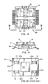
- Cover 10 preferably comprises mounting surface means 12 for mounting at least one capacitor 14 to a surface of the cover.
- Mounting surface means 12 preferably comprises metalization means 16 including a metalized power pad 20 and a metalized ground pad 22 for mounting a plurality of capacitors on a surface of the cover.
- Metalization means 16 may comprise electrically conductive castellations 26 for connecting both metalized power pad 20 and metalized ground pad 22 to semiconductor chip package power and ground connections.
- metalization means may comprise metal clips 30, illustrated in Figure 8, or vias 34, illustrated in Figure 4, for connecting metalized power pad 20 to a semiconductor chip package power connection, and for connecting metalized ground pad 22 to a semiconductor chip package ground connection.
- FIG. 2 is a perspective view of preferred cover 10 shown with a plurality of capacitors 14 electrically connected between power pad 20 and ground pads 22. As illustrated, the number of capacitors that are placed on mounting surface means 12 may vary. Moreover, the ability to place numerous small capacitors, which are less susceptible to cracking, on mounting surface means 12, substantially enhances the reliability of cover 10 and capacitors 14 during thermal cycling.
- Preferred cover 10 includes castellations 26 providing an electrically conductive path to other portions of cover 10 and the semiconductor chip package.
- FIG. 3 is a perspective view of the bottom portion of cover 10.
- Preferred cover 10 bottom portion comprises region 36 comprising an optional cavity constructed and arranged for covering a semiconductor chip.
- Sealing surface 38 extends peripherally around region 36 and provides means for sealing cover 10 to a semiconductor chip package surface.
- Sealing surface 38 is typically comprised of tungsten which has been nickel and gold plated, although other conductive materials could be used.
- Cover 10 metalization means 16 may also comprise an integral power plane 42 and ground plane 44 as shown in Figure 4. As illustrated in Figures 1 and 4, cover 10 may comprise metalization means comprising castellations 26 for connecting metalized power pad 20 to integral power plane 42 and for connecting integral power plane 42 to a semiconductor chip package power connection. Similarly, metalization means may comprise castellations 26 for connecting metalized ground pad 22 to integral ground plane 44 and for connecting integral ground plane 44 to a semiconductor chip package ground connection.
- Alternate metalization means 16 is shown in Figures 4 and 5. Alternate metalization means 16 comprises vias 34 for connecting metalized power pads 20 to integral power plane 42 and for connecting integral power plane 42 to a semiconductor chip package power connection. Similarly, metalization means 16 illustrated in Figures 4 and 5 includes vias 34 for connecting metalized ground pads 22 to integral ground plane 44 and for connecting integral ground plane 44 to a semiconductor chip package ground connection.
- Figure 6 is a perspective view of a bottom surface of cover 10 configured with vias 34 and chip covering region 36. Sealing surface 38 extends around region 36 and provides means for covering a semiconductor chip.
- Figure 7 illustrates a side elevation view of multi-chip capacitor cover 10 having multiple capacitors 14 mounted thereon.
- Capacitors 14 are shown electrically connected to semiconductor chip means 48 by metalization means 16.
- Metalization means 16 comprises vias 34 for connecting capacitors 14 to integral power plane 42 and integral ground plane 44. Vias 34 also provide means for connecting the power plane 42 and ground plane 44 to respective power and ground connections on semiconductor chip package 50.
- Figure 8 is a top plan view of a representative semiconductor chip package 60 having a chip retaining section therein (not shown) and a multi-chip capacitor cover 10 having multiple capacitors 14 mounted thereon.
- Figure 9 is a side elevation view of Figure 8 which shows a manner of attaching metal clips 30 onto package 60 and cover 10 between ground pads 22 and power pads 20. Use of metal clips 30 permits rapid assembly of components as well as low cost options for varied cover 10 capacitance configurations.
- multi-chip capacitor cover 10 comprises means for mounting capacitors directly above active devices to provide capacitive means in various combinations.
- the various embodiments of cover 10 permit flexible arrangements of capacitors in close proximity to active devices independent of thermal coefficient problems usually caused by different material characteristics of capacitors and chip covers. Accordingly, multi-chip capacitor cover 10 provides for improved noise reduction independent of thermal coefficient mismatch difficulties caused by adjacent components expanding and contracting at different rates.
- the present invention provides a significant space saving advantage over typical prior art semiconductor chip package designs such as package 70 illustrated in Figure 10.
- package 70 the package itself comprises metalization regions surrounding typical prior art package covers such as 10a for mounting capacitors 14.
- metalized regions typically included metalized power pads 20a and metalized ground pads 22a for mounting capacitors 14 surrounding typical prior art covers 10a.
- prior art packages 70 were required to be considerably larger than packages utilizing the present invention, since significant space savings is provided through the present invention by incorporating mounting surface means for mounting a capacitor 14 to the surface of a cover 10, there being no need for configuring packages using the present invention to include space for capacitors 14 surrounding prior art covers such as 10a.
Landscapes
- Semiconductor Integrated Circuits (AREA)
- Shielding Devices Or Components To Electric Or Magnetic Fields (AREA)
- Cooling Or The Like Of Semiconductors Or Solid State Devices (AREA)
Applications Claiming Priority (2)
| Application Number | Priority Date | Filing Date | Title |
|---|---|---|---|
| US348999 | 1989-05-08 | ||
| US07/348,999 US5043533A (en) | 1989-05-08 | 1989-05-08 | Chip package capacitor cover |
Publications (2)
| Publication Number | Publication Date |
|---|---|
| EP0397391A2 true EP0397391A2 (de) | 1990-11-14 |
| EP0397391A3 EP0397391A3 (de) | 1991-12-04 |
Family
ID=23370456
Family Applications (1)
| Application Number | Title | Priority Date | Filing Date |
|---|---|---|---|
| EP19900304810 Withdrawn EP0397391A3 (de) | 1989-05-08 | 1990-05-03 | Chippackung mit Kondensatordeckel |
Country Status (4)
| Country | Link |
|---|---|
| US (1) | US5043533A (de) |
| EP (1) | EP0397391A3 (de) |
| JP (1) | JPH0362954A (de) |
| CA (1) | CA2014255C (de) |
Cited By (4)
| Publication number | Priority date | Publication date | Assignee | Title |
|---|---|---|---|---|
| DE4242097A1 (de) * | 1992-12-14 | 1994-06-16 | Bosch Gmbh Robert | Anordnung zum elektromagnetischen Verträglichkeits(EMV)-Schutz von Hybridbauelementen |
| EP0841699A3 (de) * | 1996-11-08 | 1999-03-10 | Shinko Electric Industries Co. Ltd. | Filmkapazität und Halbleiterpackung oder Anordnung damit |
| EP1001464A1 (de) * | 1998-11-09 | 2000-05-17 | Robert Bosch Gmbh | Monolithisch integrierte Schaltung mit mehreren Kapazitäten |
| DE19728692C2 (de) * | 1997-07-04 | 2002-04-11 | Infineon Technologies Ag | IC-Baustein mit passiven Bauelementen |
Families Citing this family (12)
| Publication number | Priority date | Publication date | Assignee | Title |
|---|---|---|---|---|
| US5270488A (en) * | 1990-07-27 | 1993-12-14 | Mitsubishi Denki Kabushiki Kaisha | Shield construction for electrical devices |
| JP2772184B2 (ja) * | 1991-11-07 | 1998-07-02 | 株式会社東芝 | 半導体装置 |
| JP2704076B2 (ja) * | 1991-11-14 | 1998-01-26 | 甲府日本電気株式会社 | 集積回路パッケージ |
| US5155656A (en) * | 1991-12-12 | 1992-10-13 | Micron Technology, Inc. | Integrated series capacitors for high reliability electronic applications including decoupling circuits |
| US5280413A (en) * | 1992-09-17 | 1994-01-18 | Ceridian Corporation | Hermetically sealed circuit modules having conductive cap anchors |
| WO1995031826A1 (en) * | 1994-05-17 | 1995-11-23 | Olin Corporation | Electronic packages with improved electrical performance |
| US5844419A (en) * | 1996-05-14 | 1998-12-01 | Micron Technology, Inc. | Method for testing semiconductor packages using decoupling capacitors to reduce noise |
| US6175241B1 (en) | 1999-02-19 | 2001-01-16 | Micron Technology, Inc. | Test carrier with decoupling capacitors for testing semiconductor components |
| KR100618903B1 (ko) * | 2005-06-18 | 2006-09-01 | 삼성전자주식회사 | 독립된 전원 장치를 구비하는 반도체 집적 회로와 반도체집적 회로를 구비하는 반도체 시스템 및 반도체 집적 회로형성 방법 |
| US8012874B2 (en) * | 2007-12-14 | 2011-09-06 | Ati Technologies Ulc | Semiconductor chip substrate with multi-capacitor footprint |
| US8564122B2 (en) | 2011-12-09 | 2013-10-22 | Advanced Micro Devices, Inc. | Circuit board component shim structure |
| US11837527B2 (en) | 2020-07-23 | 2023-12-05 | Advanced Micro Devices, Inc. | Semiconductor chip stack with locking through vias |
Family Cites Families (11)
| Publication number | Priority date | Publication date | Assignee | Title |
|---|---|---|---|---|
| US3833753A (en) * | 1972-11-30 | 1974-09-03 | V Garboushian | Hermetically sealed mounting structure for miniature electronic circuitry |
| US4249196A (en) * | 1978-08-21 | 1981-02-03 | Burroughs Corporation | Integrated circuit module with integral capacitor |
| US4451845A (en) * | 1981-12-22 | 1984-05-29 | Avx Corporation | Lead frame device including ceramic encapsulated capacitor and IC chip |
| US4636918A (en) * | 1982-07-30 | 1987-01-13 | Rogers Corporation | Decoupled integrated circuit package |
| JPS5954249A (ja) * | 1982-09-22 | 1984-03-29 | Fujitsu Ltd | 半導体装置 |
| JPS5972751A (ja) * | 1982-10-20 | 1984-04-24 | Fujitsu Ltd | 半導体装置 |
| JPS59111350A (ja) * | 1982-12-16 | 1984-06-27 | Matsushita Electric Ind Co Ltd | 半導体装置 |
| FR2550009B1 (fr) * | 1983-07-29 | 1986-01-24 | Inf Milit Spatiale Aeronaut | Boitier de composant electronique muni d'un condensateur |
| US4672421A (en) * | 1984-04-02 | 1987-06-09 | Motorola, Inc. | Semiconductor packaging and method |
| FR2565032B1 (fr) * | 1984-05-25 | 1987-02-20 | Inf Milit Spatiale Aeronaut | Dispositif de repartition de potentiel electrique et boitier de composant electronique incorporant un tel dispositif |
| JPS61108160A (ja) * | 1984-11-01 | 1986-05-26 | Nec Corp | コンデンサ内蔵型半導体装置及びその製造方法 |
-
1989
- 1989-05-08 US US07/348,999 patent/US5043533A/en not_active Expired - Lifetime
-
1990
- 1990-04-10 CA CA002014255A patent/CA2014255C/en not_active Expired - Lifetime
- 1990-05-03 EP EP19900304810 patent/EP0397391A3/de not_active Withdrawn
- 1990-05-08 JP JP2117016A patent/JPH0362954A/ja active Pending
Cited By (8)
| Publication number | Priority date | Publication date | Assignee | Title |
|---|---|---|---|---|
| DE4242097A1 (de) * | 1992-12-14 | 1994-06-16 | Bosch Gmbh Robert | Anordnung zum elektromagnetischen Verträglichkeits(EMV)-Schutz von Hybridbauelementen |
| DE4242097C2 (de) * | 1992-12-14 | 2001-03-01 | Bosch Gmbh Robert | Anordnung zum elektromagnetischen Verträglichkeits(EMV)-Schutz von Hybridbauelementen |
| EP0841699A3 (de) * | 1996-11-08 | 1999-03-10 | Shinko Electric Industries Co. Ltd. | Filmkapazität und Halbleiterpackung oder Anordnung damit |
| KR100277314B1 (ko) * | 1996-11-08 | 2001-01-15 | 모기 쥰이찌 | 박막콘덴서 및 이를탑재한반도체장치 |
| US6184567B1 (en) | 1996-11-08 | 2001-02-06 | Shinko Electric Industries Co., Ltd. | Film capacitor and semiconductor package or device carrying same |
| DE19728692C2 (de) * | 1997-07-04 | 2002-04-11 | Infineon Technologies Ag | IC-Baustein mit passiven Bauelementen |
| EP1001464A1 (de) * | 1998-11-09 | 2000-05-17 | Robert Bosch Gmbh | Monolithisch integrierte Schaltung mit mehreren Kapazitäten |
| US6469331B2 (en) | 1998-11-09 | 2002-10-22 | Robert Bosch Gmbh | Monolithic integrated circuit with several capacitors forming bypass to ground |
Also Published As
| Publication number | Publication date |
|---|---|
| CA2014255C (en) | 2000-12-26 |
| EP0397391A3 (de) | 1991-12-04 |
| US5043533A (en) | 1991-08-27 |
| CA2014255A1 (en) | 1990-11-08 |
| JPH0362954A (ja) | 1991-03-19 |
Similar Documents
| Publication | Publication Date | Title |
|---|---|---|
| US5043533A (en) | Chip package capacitor cover | |
| US4939570A (en) | High power, pluggable tape automated bonding package | |
| US5384488A (en) | Configuration and method for positioning semiconductor device bond pads using additional process layers | |
| US5563446A (en) | Surface mount peripheral leaded and ball grid array package | |
| US4783697A (en) | Leadless chip carrier for RF power transistors or the like | |
| JP4437919B2 (ja) | 電子部品パッケージ用emi遮蔽 | |
| US5528083A (en) | Thin film chip capacitor for electrical noise reduction in integrated circuits | |
| US5521435A (en) | Semiconductor device and a fabrication process thereof | |
| KR100328143B1 (ko) | 계층화된 도전 평면을 갖는 리드 프레임 | |
| US20060180345A1 (en) | Perimeter matrix ball grid array circuit package with a populated center | |
| US5067005A (en) | Semiconductor device | |
| US5497031A (en) | Semiconductor device having semiconductor chip with backside electrode | |
| KR100328906B1 (ko) | 리드프레임의리드온칩내부리드를결합하는방법및장치 | |
| EP0863549B1 (de) | Halbleiteranordnung mit einem Leitersubstrat | |
| KR20010034154A (ko) | 다수의 기판층과 적어도 하나의 반도체 칩을 가진 반도체소자 및 그의 제조 방법 | |
| KR960012647B1 (ko) | 반도체장치 및 그 제조방법 | |
| US5545921A (en) | Personalized area leadframe coining or half etching for reduced mechanical stress at device edge | |
| US5455387A (en) | Semiconductor package with chip redistribution interposer | |
| US6320757B1 (en) | Electronic package | |
| US5523621A (en) | Semiconductor device having a multilayer ceramic wiring substrate | |
| US6166435A (en) | Flip-chip ball grid array package with a heat slug | |
| US5220196A (en) | Semiconductor device | |
| JPH0774278A (ja) | セラミック・パッケージ組立部品 | |
| US5719748A (en) | Semiconductor package with a bridge for chip area connection | |
| US4380357A (en) | System and method for effecting electrical interconnections using a flexible media with radially extending electrical conductors |
Legal Events
| Date | Code | Title | Description |
|---|---|---|---|
| PUAI | Public reference made under article 153(3) epc to a published international application that has entered the european phase |
Free format text: ORIGINAL CODE: 0009012 |
|
| AK | Designated contracting states |
Kind code of ref document: A2 Designated state(s): DE FR GB |
|
| PUAL | Search report despatched |
Free format text: ORIGINAL CODE: 0009013 |
|
| AK | Designated contracting states |
Kind code of ref document: A3 Designated state(s): DE FR GB |
|
| 17P | Request for examination filed |
Effective date: 19920615 |
|
| 17Q | First examination report despatched |
Effective date: 19940217 |
|
| RAP1 | Party data changed (applicant data changed or rights of an application transferred) |
Owner name: SAMSUNG ELECTRONICS CO., LTD. |
|
| STAA | Information on the status of an ep patent application or granted ep patent |
Free format text: STATUS: THE APPLICATION IS DEEMED TO BE WITHDRAWN |
|
| 18D | Application deemed to be withdrawn |
Effective date: 19960220 |