EP0397476A2 - Système d'enregistrement de données d'erreur - Google Patents
Système d'enregistrement de données d'erreur Download PDFInfo
- Publication number
- EP0397476A2 EP0397476A2 EP90305006A EP90305006A EP0397476A2 EP 0397476 A2 EP0397476 A2 EP 0397476A2 EP 90305006 A EP90305006 A EP 90305006A EP 90305006 A EP90305006 A EP 90305006A EP 0397476 A2 EP0397476 A2 EP 0397476A2
- Authority
- EP
- European Patent Office
- Prior art keywords
- logging data
- error logging
- error
- storing
- signal
- Prior art date
- Legal status (The legal status is an assumption and is not a legal conclusion. Google has not performed a legal analysis and makes no representation as to the accuracy of the status listed.)
- Granted
Links
Images


Classifications
-
- G—PHYSICS
- G06—COMPUTING OR CALCULATING; COUNTING
- G06F—ELECTRIC DIGITAL DATA PROCESSING
- G06F11/00—Error detection; Error correction; Monitoring
- G06F11/30—Monitoring
-
- G—PHYSICS
- G06—COMPUTING OR CALCULATING; COUNTING
- G06F—ELECTRIC DIGITAL DATA PROCESSING
- G06F11/00—Error detection; Error correction; Monitoring
- G06F11/07—Responding to the occurrence of a fault, e.g. fault tolerance
- G06F11/0703—Error or fault processing not based on redundancy, i.e. by taking additional measures to deal with the error or fault not making use of redundancy in operation, in hardware, or in data representation
- G06F11/0766—Error or fault reporting or storing
- G06F11/0772—Means for error signaling, e.g. using interrupts, exception flags, dedicated error registers
-
- G—PHYSICS
- G06—COMPUTING OR CALCULATING; COUNTING
- G06F—ELECTRIC DIGITAL DATA PROCESSING
- G06F11/00—Error detection; Error correction; Monitoring
- G06F11/07—Responding to the occurrence of a fault, e.g. fault tolerance
- G06F11/0703—Error or fault processing not based on redundancy, i.e. by taking additional measures to deal with the error or fault not making use of redundancy in operation, in hardware, or in data representation
- G06F11/0706—Error or fault processing not based on redundancy, i.e. by taking additional measures to deal with the error or fault not making use of redundancy in operation, in hardware, or in data representation the processing taking place on a specific hardware platform or in a specific software environment
- G06F11/0721—Error or fault processing not based on redundancy, i.e. by taking additional measures to deal with the error or fault not making use of redundancy in operation, in hardware, or in data representation the processing taking place on a specific hardware platform or in a specific software environment within a central processing unit [CPU]
- G06F11/0724—Error or fault processing not based on redundancy, i.e. by taking additional measures to deal with the error or fault not making use of redundancy in operation, in hardware, or in data representation the processing taking place on a specific hardware platform or in a specific software environment within a central processing unit [CPU] in a multiprocessor or a multi-core unit
-
- G—PHYSICS
- G06—COMPUTING OR CALCULATING; COUNTING
- G06F—ELECTRIC DIGITAL DATA PROCESSING
- G06F11/00—Error detection; Error correction; Monitoring
- G06F11/07—Responding to the occurrence of a fault, e.g. fault tolerance
- G06F11/0703—Error or fault processing not based on redundancy, i.e. by taking additional measures to deal with the error or fault not making use of redundancy in operation, in hardware, or in data representation
- G06F11/0766—Error or fault reporting or storing
- G06F11/0781—Error filtering or prioritizing based on a policy defined by the user or on a policy defined by a hardware/software module, e.g. according to a severity level
Definitions
- the present invention relates to an error logging data storing system which is provided between a data processing system and a service processor which is provided for diagnosing errors occurring in the data processing system for maintenance support.
- the data processing system stops by itself, and informs the error logging data storing system of the error for sending error logging data thereto.
- the error logging data is stored in the error logging data storing system until the diagnosing operation of the error logging data by the service processor is completed.
- the provision of the error logging data storing system between the data processing system and the service processor enables the data processing system to restart its operation before the completion of the diagnosing operation of the error logging data by the service processor.
- a plurality of memory areas are provided corresponding to degrees of importance of errors.
- two memory areas are provided and are exclusively used for storing error logging data corresponding to errors of high importance which bring the data processing system into a down state, and errors of low importance which do not bring the data processing system into a down state.
- the provision of the plurality of memory areas for respective degrees of importance of the errors facilitates the diagnosing operation by the service processor.
- an error logging data storing system containing: a first storing unit for storing error logging data corresponding to an error of high importance; a second storing unit for storing error logging data corresponding to an error of either high or low importance; a first indicating unit for indicating whether or not the first storing unit is occupied by error logging data the diagnosing operation of which is not completed; a second indicating unit for indicating whether or not the second storing unit is occupied by error logging data the diagnosing operation of which is not completed; and a storage control unit for storing error logging data corresponding to an error of high importance in the second storing unit when the first indicating unit indicates that the first storing unit is occupied by error logging data the diagnosing operation of which is not completed, and the second indicating unit indicates that the second storing unit is not occupied by error logging data the diagnosing operation of which is not completed
- the above error logging data storing system further can comprise a third indicating unit for indicating degree of importance of the error corresponding to error logging data which is stored in the second storing unit.
- the above error logging data storing system further can comprise an access control unit for transferring error logging data from a data processor to either of the first and second storing unit.
- the above error logging data storing system further can comprise a transfer completion informing unit for informing completion of a transfer operation of error logging data, to a data processor from which the error logging data has been transferred.
- the above error logging data storing system further can comprise an impossibility informing unit for informing impossibility of a transfer operation of error logging data, to a data processor from which a request for storing the error logging data has been sent.
- the above error logging data storing system further can comprise a priority control unit for receiving a request for storing error logging data, which is first sent thereto, among requests for storing error logging data, which are sent from a plurality of data processors, a first processor indicating unit for indicating from which of the plurality of data processors the error logging data is stored in the first storing unit, and a second processor indicating unit for indicating from which of the plurality of data processors the error logging data is stored in the second storing unit.
- a priority control unit for receiving a request for storing error logging data, which is first sent thereto, among requests for storing error logging data, which are sent from a plurality of data processors, a first processor indicating unit for indicating from which of the plurality of data processors the error logging data is stored in the first storing unit, and a second processor indicating unit for indicating from which of the plurality of data processors the error logging data is stored in the second storing unit.
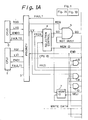
- Figure 1 shows the construction of an embodiment of the present invention.
- reference numerals 0 and 1 respectively denote a central processing unit
- 3 denotes a priority control circuit
- 4 denotes a selection control circuit
- 5, 8, 9, 10, 14 and 15 each denote an AND circuit
- 6 denotes an access control circuit
- 7 denotes an accessing memory indication register
- 11 and 16 each denote first and second CPU indication registers
- 12 denotes a memory occupying error level indication register
- 13 and 17 each denote a first and second freezing status register
- 18 and 19 each denote a memory unit
- 20 denotes a status register
- 21 denotes a service processor.
- the CPU's 0 and 1 are processors in a multi-processor data processing system, and the errors which occur in the data processing system are diagnosed by the service processor 21.
- the CPU's 0 and 1 each have a function to detect an occurrence of an error in its own processor, stop its operation, and send a request for transferring error logging data regarding the error, together with information on the degree of importance of the error, to the error logging data storing system.
- the CPU receives a signal which indicates that the requested transfer operation is completed, or a signal which indicates that the requested transfer operation is impossible, from the error logging data storing system, the CPU restarts its operation.
- the memory unit 18 is provided for storing error logging data corresponding to an error of high importance
- the memory unit 19 is provided for storing error logging data corresponding to an error of either high or low importance.
- RQ0 denotes a request for transferring error logging data from the CPU
- RQ1 denotes a request for transferring error logging data from the CPU
- LV0 denotes information on the degree of importance of the error occurring in the CPU
- LV1 denotes information on the degree of importance of the error occurring in the CPU 1
- END0 denotes the signal to the CPU 0 indicating that the requested transfer operation is completed
- END1 denotes the signal to the CPU 1 indicating that the requested transfer operation is completed
- FAULT0 denotes the signal to the CPU 0 indicating that the requested transfer operation is impossible
- FAULT1 denotes the signal to the CPU 1 indicating that the requested transfer operation is impossible.
- the above-mentioned request and the above-mentioned information on the degree of importance from each CPU, are applied to the priority control circuit 3 in the error logging data storing system.
- the priority control circuit 3 in the error logging data storing system receives a first applied one of the above-mentioned requests RQ0 and RQ1 and the above-mentioned information LV0 or LV1 on the degree of importance accompanying the request.
- the request which is applied to the priority control circuit 3 next to the last received request can be received by the priority control circuit 3 after the transfer operation of the error logging data for the last received request is completed, or after the transfer operation of the error logging data for the last received request is determined to be impossible.
- the priority control circuit 3 outputs a REQ signal which indicates that a request for transferring error logging data from a CPU is received, a LV signal which indicates the degree of importance of the error corresponding to the received request, and a CPU ID signal which indicates from which CPU the request is received.
- the LV signal is “0" when the degree of importance is high, or is “1” when the degree of importance is low.
- the CPU ID signal is “0” when the request is received from the CPU 0, or is “1" when the request is received from the CPU 1.
- the priority control circuit 3 receives an END signal which indicates that the transfer operation of the error logging data for the received request to the error logging data storing system is completed, and a FAULT signal which indicates that the error logging data for the received request cannot be transferred to the error logging data storing system, in the error logging data storing system.
- the CPU ID signal is set to "0", and the LV0 signal from the CPU 0 is selected as the LV signal output.
- the CPU ID signal is set to '1' , and the LV1 signal from the CPU 1 is selected as the LV signal output.
- the END signal is output as the END0 signal, and the FAULT signal is output as the FAULT0 signal.
- the END signal is output as the END1 signal, and the FAULT signal is output as the FAULT1 signal.
- the selection control circuit 4 receives the above LV signal, and FRZ0 and FRZ1 signals respectively indicating whether or not the memory units 18 and 19 are occupied by error logging data the diagnosing operations of which are not completed yet.
- the selection control circuit 4 determines whether or not the error logging data for the received request can be stored in the error logging data storing system, and which memory unit the error logging data is to be stored, based on the above inputs.
- the selection control circuit 4 outputs an active GO signal, or when it is determined that the error logging data for the received request cannot be stored in the error logging data storing system, the selection control circuit 4 outputs an active FAULT signal.
- FIG. 2 The construction of the selection control circuit 4 is shown in Fig. 2.
- reference numerals 30, 31, and 32 each denote an AND circuit
- 33 and 34 each denote an OR circuit
- 35, 36, and 37 each denote an inverter.
- the LV signal and the inverted FRZ1 signal are applied to the AND circuit 30, the inverted LV signal and the inverted FRZ0 signal are applied to the AND circuit 31, and the inverted LV signal, the inverted FRZ1 signal, and the FRZ0 signal are applied to the AND circuit 32.
- the outputs of the AND circuits 30, 31, and 32 are applied to the OR circuit 33, and the outputs of the AND circuits 30 and 32 are applied to the OR circuit 34.
- the positive logic output of the OR circuit 33 is output as the GO signal, and the negative logic output of the OR circuit 33 is output as the FAULT signal.
- the output of the OR circuit 34 is output as a MEM ID signal which is "0" when it is determined that the error logging data is to be stored in the memory unit 18, or is "1" when it is determined that the error logging data is to be stored in the memory unit 19.
- the access control circuit 6 generates address signals of registers in turns in the CPU from which the request is received to output error logging data from the registers, when a GO signal is applied from the AND circuit 5.
- each CPU contains a construction for decoding the above address, and outputting the content of the register which is addressed toward the error logging data storing system.
- an error logging data transferring line is provided which is exclusively used for transferring error logging data from each register to the error logging data storing system.
- the access control circuit 6 outputs a read address to the memory unit to which error logging data is determined to be stored, based on the above-mentioned MEM ID signal.
- the MEM ID signal from the selection control circuit 4 is input into both the access control circuit 6 and the accessing memory indication register 7.
- the output of the accessing memory indication register 7 is applied to the memory units 18 and 19 as a chip select signal which makes one of the memory units 18 and 19 active in accordance with the MEM ID signal.
- the access control circuit 6 further outputs a NOT BUSY signal which is inactive during the above address output operation for the transfer operation of error logging data between a CPU and the error logging data storing system.
- a NOT BUSY signal which is inactive during the above address output operation for the transfer operation of error logging data between a CPU and the error logging data storing system.
- the above NOT BUSY signal is applied to the AND circuit 5 together with the REQ signal from the priority control circuit 3 and the GO signal from the selection control circuit 4.
- the GO signal is applied to the access control circuit 6.
- the END signal from the access control circuit 6 is applied to the priority control circuit 3, and the AND circuits 8, 9, 10, 14, and 15.
- the applications of the END signal to the AND circuits make respective registers corresponding to the AND circuits latch status when a transfer operation of error logging data is completed.
- the AND circuit 8 further receives a negative output of the accessing memory indication register 7 which is "1" when the MEM ID signal is "0", and the CPU ID signal. The output of the AND circuit 8 is latched in the first CPU indication register 11.
- the AND circuit 14 further receives a positive output of the accessing memory indication register 7 which is "1" when the MEM ID signal is “1", and the CPU ID signal. The output of the AND circuit 14 is latched in the first CPU indication register 16.
- the number indicating the CPU from which error logging data is transferred to the memory unit 18 is latched in the first CPU indication register 11 after the transfer operation of error logging data to the memory unit 18 is completed, or is latched in the second CPU indication register 16 after the transfer operation of error logging data to the memory unit 19 is completed.
- the AND circuit 9 further receives a positive output of the accessing memory indication register 7, and the LV signal.
- the output of the AND circuit 9 is latched in the memory occupying error level indication register 12.
- the LV signal is latched in the memory occupying error level indication register 12 after the transfer operation of error logging data to the memory unit 19, is completed, i.e., the output of the memory occupying error level indication register 12 indicates the degree of importance of the error corresponding to the error logging data which is stored in the memory unit 19.
- the AND circuit 10 further receives a negative output of the accessing memory indication register 7 which is "1" when the MEM ID signal is "0", and the CPU ID signal.
- the output of the AND circuit 10 is latched in the first freezing status register 13.
- the AND circuit 15 further receives a positive output of the accessing memory indication register 7 which is "1" when the MEM ID signal is “1", and the CPU ID signal.
- the output of the AND circuit 15 is latched in the second freezing status register 17. Namely, "1" is latched in the first freezing status register 13 after the transfer operation of error logging data to the memory unit 18 is completed, and "1" is latched in the second freezing status register 17 after the transfer operation of error logging data to the memory unit 18 is completed.
- the outputs of the first and second CPU indication registers 11 and 16, the memory occupying error level indication register 12, and the first and second freezing status registers 13 and 17, are latched in the status register 20.
- the statuses relating to the memory unit 18, are reset by service processor 21 when each diagnosing operation of the error logging data stored in the memory unit 18 is completed, and the statuses relating to the memory unit 19, are reset by service processor 21 when each diagnosing operation of the error logging data stored in the memory unit 19 is completed.
- the service processor 21 reads the error logging data stored in each memory units 18 or 19.
- the service processor 21 sends a memory read command to the access control circuit 6, and a memory selection signal to the accessing memory indication register 7.
- Receiving the memory selection signal one of the memory unit 18 or 19, which is instructed by the memory selection signal, is made active by the negative or positive output of the accessing memory indication register 7.
- the access control circuit 6 outputs addresses for reading the error logging data stored in the memory unit 18 or 19 which is instructed by the memory selection signal, to read the error logging data therein to the service processor 21.
- error logging data corresponding to an error of high importance can be stored in the memory area which is conventionally provided for storing error logging data corresponding to an error of high importance, and thus the capacity for error logging data corresponding to errors of high importance can be flexibly increased.
Landscapes
- Engineering & Computer Science (AREA)
- Theoretical Computer Science (AREA)
- Quality & Reliability (AREA)
- Physics & Mathematics (AREA)
- General Engineering & Computer Science (AREA)
- General Physics & Mathematics (AREA)
- Debugging And Monitoring (AREA)
- Test And Diagnosis Of Digital Computers (AREA)
Applications Claiming Priority (2)
| Application Number | Priority Date | Filing Date | Title |
|---|---|---|---|
| JP117996/89 | 1989-05-11 | ||
| JP1117996A JPH02297228A (ja) | 1989-05-11 | 1989-05-11 | 障害情報格納方式 |
Publications (3)
| Publication Number | Publication Date |
|---|---|
| EP0397476A2 true EP0397476A2 (fr) | 1990-11-14 |
| EP0397476A3 EP0397476A3 (fr) | 1992-12-30 |
| EP0397476B1 EP0397476B1 (fr) | 1996-10-23 |
Family
ID=14725459
Family Applications (1)
| Application Number | Title | Priority Date | Filing Date |
|---|---|---|---|
| EP90305006A Expired - Lifetime EP0397476B1 (fr) | 1989-05-11 | 1990-05-09 | Système d'enregistrement de données d'erreur |
Country Status (6)
| Country | Link |
|---|---|
| US (1) | US5155731A (fr) |
| EP (1) | EP0397476B1 (fr) |
| JP (1) | JPH02297228A (fr) |
| KR (1) | KR930008688B1 (fr) |
| AU (1) | AU614232B2 (fr) |
| DE (1) | DE69028945T2 (fr) |
Cited By (1)
| Publication number | Priority date | Publication date | Assignee | Title |
|---|---|---|---|---|
| EP0646713A4 (fr) * | 1992-08-11 | 1994-10-24 | Nippon Denso Co | Dispositif d'autodiagnostic pour vehicule. |
Families Citing this family (28)
| Publication number | Priority date | Publication date | Assignee | Title |
|---|---|---|---|---|
| JPH0536259A (ja) * | 1991-07-27 | 1993-02-12 | Sony Corp | 電子機器 |
| US5956352A (en) * | 1992-04-24 | 1999-09-21 | Digital Equipment Corporation | Adjustable filter for error detecting and correcting system |
| US5491788A (en) * | 1993-09-10 | 1996-02-13 | Compaq Computer Corp. | Method of booting a multiprocessor computer where execution is transferring from a first processor to a second processor based on the first processor having had a critical error |
| US5619644A (en) * | 1995-09-18 | 1997-04-08 | International Business Machines Corporation | Software directed microcode state save for distributed storage controller |
| US5862316A (en) * | 1996-07-01 | 1999-01-19 | Sun Microsystems, Inc. | Multiprocessing system having coherency-related error logging capabilities |
| US6536000B1 (en) | 1999-10-15 | 2003-03-18 | Sun Microsystems, Inc. | Communication error reporting mechanism in a multiprocessing computer system |
| US6598179B1 (en) * | 2000-03-31 | 2003-07-22 | International Business Machines Corporation | Table-based error log analysis |
| US6647517B1 (en) * | 2000-04-27 | 2003-11-11 | Hewlett-Packard Development Company, L.P. | Apparatus and method for providing error ordering information and error logging information |
| US7346812B1 (en) * | 2000-04-27 | 2008-03-18 | Hewlett-Packard Development Company, L.P. | Apparatus and method for implementing programmable levels of error severity |
| US6701464B2 (en) * | 2001-03-01 | 2004-03-02 | International Business Machines Corporation | Method and system for reporting error logs within a logical partition environment |
| US7360114B2 (en) * | 2003-06-17 | 2008-04-15 | International Business Machines Corporation | Logging of exception data |
| US8302111B2 (en) | 2003-11-24 | 2012-10-30 | Time Warner Cable Inc. | Methods and apparatus for hardware registration in a network device |
| US7266726B1 (en) | 2003-11-24 | 2007-09-04 | Time Warner Cable Inc. | Methods and apparatus for event logging in an information network |
| US7213176B2 (en) * | 2003-12-10 | 2007-05-01 | Electronic Data Systems Corporation | Adaptive log file scanning utility |
| US9213538B1 (en) | 2004-02-06 | 2015-12-15 | Time Warner Cable Enterprises Llc | Methods and apparatus for display element management in an information network |
| US8078669B2 (en) | 2004-02-18 | 2011-12-13 | Time Warner Cable Inc. | Media extension apparatus and methods for use in an information network |
| US7802145B1 (en) * | 2004-05-18 | 2010-09-21 | Cisco Technology, Inc. | Approach for facilitating analysis of computer software errors |
| JP4641443B2 (ja) * | 2005-03-28 | 2011-03-02 | 富士通株式会社 | ログ情報管理装置、ログ情報管理方法およびログ情報管理プログラム |
| JP4478196B2 (ja) | 2006-02-28 | 2010-06-09 | 富士通株式会社 | 監視装置、監視プログラム、および情報処理システム |
| US8370818B2 (en) | 2006-12-02 | 2013-02-05 | Time Warner Cable Inc. | Methods and apparatus for analyzing software interface usage |
| JP5401903B2 (ja) * | 2008-10-03 | 2014-01-29 | 富士通株式会社 | 故障情報監視装置及び故障情報監視方法 |
| JP2017091456A (ja) * | 2015-11-17 | 2017-05-25 | 富士通株式会社 | 制御装置、制御プログラムおよび制御方法 |
| US11716558B2 (en) | 2018-04-16 | 2023-08-01 | Charter Communications Operating, Llc | Apparatus and methods for integrated high-capacity data and wireless network services |
| US11044597B2 (en) | 2018-08-07 | 2021-06-22 | Charter Communications Operating, Llc | Apparatus and methods for registration and operation in wireless networks |
| US11129213B2 (en) | 2018-10-12 | 2021-09-21 | Charter Communications Operating, Llc | Apparatus and methods for cell identification in wireless networks |
| US10980025B2 (en) | 2019-01-31 | 2021-04-13 | Charter Communications Operating, Llc | Methods and apparatus for frequency transition management in a quasi-licensed wireless system |
| US11129171B2 (en) | 2019-02-27 | 2021-09-21 | Charter Communications Operating, Llc | Methods and apparatus for wireless signal maximization and management in a quasi-licensed wireless system |
| US11026205B2 (en) | 2019-10-23 | 2021-06-01 | Charter Communications Operating, Llc | Methods and apparatus for device registration in a quasi-licensed wireless system |
Family Cites Families (9)
| Publication number | Priority date | Publication date | Assignee | Title |
|---|---|---|---|---|
| US4091455A (en) * | 1976-12-20 | 1978-05-23 | Honeywell Information Systems Inc. | Input/output maintenance access apparatus |
| US4174537A (en) * | 1977-04-04 | 1979-11-13 | Burroughs Corporation | Time-shared, multi-phase memory accessing system having automatically updatable error logging means |
| US4209846A (en) * | 1977-12-02 | 1980-06-24 | Sperry Corporation | Memory error logger which sorts transient errors from solid errors |
| JPS59123058A (ja) * | 1982-12-29 | 1984-07-16 | Fujitsu Ltd | マシンチエツク処理方式 |
| US4633467A (en) * | 1984-07-26 | 1986-12-30 | At&T Bell Laboratories | Computer system fault recovery based on historical analysis |
| JPS61282944A (ja) * | 1985-06-07 | 1986-12-13 | Fujitsu Ltd | ログ縮小方式 |
| JPS63316243A (ja) * | 1987-06-19 | 1988-12-23 | Fujitsu Ltd | エラ−ログ制御方式 |
| JPS6491252A (en) * | 1987-10-01 | 1989-04-10 | Fujitsu Ltd | Error log collection processing system |
| JP2519276B2 (ja) * | 1987-12-14 | 1996-07-31 | 三菱電機株式会社 | 障害情報収集処理方式 |
-
1989
- 1989-05-11 JP JP1117996A patent/JPH02297228A/ja active Pending
-
1990
- 1990-05-07 AU AU54721/90A patent/AU614232B2/en not_active Ceased
- 1990-05-09 DE DE69028945T patent/DE69028945T2/de not_active Expired - Fee Related
- 1990-05-09 EP EP90305006A patent/EP0397476B1/fr not_active Expired - Lifetime
- 1990-05-11 US US07/522,302 patent/US5155731A/en not_active Expired - Lifetime
- 1990-05-11 KR KR1019900006692A patent/KR930008688B1/ko not_active Expired - Fee Related
Cited By (2)
| Publication number | Priority date | Publication date | Assignee | Title |
|---|---|---|---|---|
| EP0646713A4 (fr) * | 1992-08-11 | 1994-10-24 | Nippon Denso Co | Dispositif d'autodiagnostic pour vehicule. |
| US5465613A (en) * | 1992-08-11 | 1995-11-14 | Nippondenso Co., Ltd. | Self-diagnosing apparatus for motor vehicles |
Also Published As
| Publication number | Publication date |
|---|---|
| EP0397476A3 (fr) | 1992-12-30 |
| JPH02297228A (ja) | 1990-12-07 |
| EP0397476B1 (fr) | 1996-10-23 |
| DE69028945D1 (de) | 1996-11-28 |
| KR930008688B1 (ko) | 1993-09-11 |
| KR900018817A (ko) | 1990-12-22 |
| DE69028945T2 (de) | 1997-02-20 |
| AU5472190A (en) | 1990-11-15 |
| US5155731A (en) | 1992-10-13 |
| AU614232B2 (en) | 1991-08-22 |
Similar Documents
| Publication | Publication Date | Title |
|---|---|---|
| EP0397476B1 (fr) | Système d'enregistrement de données d'erreur | |
| US4130865A (en) | Multiprocessor computer apparatus employing distributed communications paths and a passive task register | |
| US4807116A (en) | Interprocessor communication | |
| US5115499A (en) | Shared computer resource allocation system having apparatus for informing a requesting computer of the identity and busy/idle status of shared resources by command code | |
| US4466098A (en) | Cross channel circuit for an electronic system having two or more redundant computers | |
| US4943966A (en) | Memory diagnostic apparatus and method | |
| US4521850A (en) | Instruction buffer associated with a cache memory unit | |
| EP0139563B1 (fr) | Mécanisme de commande pour système multi-processeur | |
| US6237108B1 (en) | Multiprocessor system having redundant shared memory configuration | |
| US3866182A (en) | System for transferring information between memory banks | |
| JPS61109164A (ja) | バス制御方法 | |
| EP0333593B1 (fr) | Système de traitement de données avec diagnostic de fautes | |
| US5634037A (en) | Multiprocessor system having a shared memory with exclusive access for a requesting processor which is maintained until normal completion of a process and for retrying the process when not normally completed | |
| US5301332A (en) | Method and apparatus for a dynamic, timed-loop arbitration | |
| EP0165823B1 (fr) | Circuit de commande d'étiquettes pour mémoire tampon | |
| EP0206657B1 (fr) | Dispositif pour la notification d'entrées/sorties à un processeur | |
| JP3052857B2 (ja) | クラスタ間共有メモリアクセス方式 | |
| CN115757196A (zh) | 内存、访问内存方法及计算设备 | |
| US4630197A (en) | Anti-mutilation circuit for protecting dynamic memory | |
| JPH1027115A (ja) | コンピュータシステムの障害情報採取回路 | |
| JP3273191B2 (ja) | データ転送装置 | |
| JP2972568B2 (ja) | バス拡張装置 | |
| JP2549849B2 (ja) | 多重化メモリ装置 | |
| JPH0237458A (ja) | 冗長バス構成のバス制御方式 | |
| JPH0116193Y2 (fr) |
Legal Events
| Date | Code | Title | Description |
|---|---|---|---|
| PUAI | Public reference made under article 153(3) epc to a published international application that has entered the european phase |
Free format text: ORIGINAL CODE: 0009012 |
|
| AK | Designated contracting states |
Kind code of ref document: A2 Designated state(s): DE ES FR GB |
|
| PUAL | Search report despatched |
Free format text: ORIGINAL CODE: 0009013 |
|
| AK | Designated contracting states |
Kind code of ref document: A3 Designated state(s): DE ES FR GB |
|
| 17P | Request for examination filed |
Effective date: 19930205 |
|
| 17Q | First examination report despatched |
Effective date: 19950519 |
|
| GRAG | Despatch of communication of intention to grant |
Free format text: ORIGINAL CODE: EPIDOS AGRA |
|
| GRAH | Despatch of communication of intention to grant a patent |
Free format text: ORIGINAL CODE: EPIDOS IGRA |
|
| RBV | Designated contracting states (corrected) |
Designated state(s): DE FR GB |
|
| GRAH | Despatch of communication of intention to grant a patent |
Free format text: ORIGINAL CODE: EPIDOS IGRA |
|
| GRAA | (expected) grant |
Free format text: ORIGINAL CODE: 0009210 |
|
| AK | Designated contracting states |
Kind code of ref document: B1 Designated state(s): DE FR GB |
|
| REF | Corresponds to: |
Ref document number: 69028945 Country of ref document: DE Date of ref document: 19961128 |
|
| ET | Fr: translation filed | ||
| PLBE | No opposition filed within time limit |
Free format text: ORIGINAL CODE: 0009261 |
|
| STAA | Information on the status of an ep patent application or granted ep patent |
Free format text: STATUS: NO OPPOSITION FILED WITHIN TIME LIMIT |
|
| 26N | No opposition filed | ||
| REG | Reference to a national code |
Ref country code: GB Ref legal event code: IF02 |
|
| PGFP | Annual fee paid to national office [announced via postgrant information from national office to epo] |
Ref country code: GB Payment date: 20040505 Year of fee payment: 15 |
|
| PGFP | Annual fee paid to national office [announced via postgrant information from national office to epo] |
Ref country code: FR Payment date: 20040510 Year of fee payment: 15 |
|
| PGFP | Annual fee paid to national office [announced via postgrant information from national office to epo] |
Ref country code: DE Payment date: 20040520 Year of fee payment: 15 |
|
| PG25 | Lapsed in a contracting state [announced via postgrant information from national office to epo] |
Ref country code: GB Free format text: LAPSE BECAUSE OF NON-PAYMENT OF DUE FEES Effective date: 20050509 |
|
| PG25 | Lapsed in a contracting state [announced via postgrant information from national office to epo] |
Ref country code: DE Free format text: LAPSE BECAUSE OF NON-PAYMENT OF DUE FEES Effective date: 20051201 |
|
| GBPC | Gb: european patent ceased through non-payment of renewal fee |
Effective date: 20050509 |
|
| PG25 | Lapsed in a contracting state [announced via postgrant information from national office to epo] |
Ref country code: FR Free format text: LAPSE BECAUSE OF NON-PAYMENT OF DUE FEES Effective date: 20060131 |
|
| REG | Reference to a national code |
Ref country code: FR Ref legal event code: ST Effective date: 20060131 |