EP0397889A1 - Lichtemittierendes Element - Google Patents
Lichtemittierendes Element Download PDFInfo
- Publication number
- EP0397889A1 EP0397889A1 EP89912672A EP89912672A EP0397889A1 EP 0397889 A1 EP0397889 A1 EP 0397889A1 EP 89912672 A EP89912672 A EP 89912672A EP 89912672 A EP89912672 A EP 89912672A EP 0397889 A1 EP0397889 A1 EP 0397889A1
- Authority
- EP
- European Patent Office
- Prior art keywords
- thin film
- layer
- luminescence
- electrode layer
- film layer
- Prior art date
- Legal status (The legal status is an assumption and is not a legal conclusion. Google has not performed a legal analysis and makes no representation as to the accuracy of the status listed.)
- Granted
Links
Images

Classifications
-
- H—ELECTRICITY
- H10—SEMICONDUCTOR DEVICES; ELECTRIC SOLID-STATE DEVICES NOT OTHERWISE PROVIDED FOR
- H10H—INORGANIC LIGHT-EMITTING SEMICONDUCTOR DEVICES HAVING POTENTIAL BARRIERS
- H10H20/00—Individual inorganic light-emitting semiconductor devices having potential barriers, e.g. light-emitting diodes [LED]
- H10H20/80—Constructional details
- H10H20/81—Bodies
- H10H20/817—Bodies characterised by the crystal structures or orientations, e.g. polycrystalline, amorphous or porous
- H10H20/818—Bodies characterised by the crystal structures or orientations, e.g. polycrystalline, amorphous or porous within the light-emitting regions
-
- H—ELECTRICITY
- H05—ELECTRIC TECHNIQUES NOT OTHERWISE PROVIDED FOR
- H05B—ELECTRIC HEATING; ELECTRIC LIGHT SOURCES NOT OTHERWISE PROVIDED FOR; CIRCUIT ARRANGEMENTS FOR ELECTRIC LIGHT SOURCES, IN GENERAL
- H05B33/00—Electroluminescent light sources
- H05B33/12—Light sources with substantially two-dimensional [2D] radiating surfaces
- H05B33/14—Light sources with substantially two-dimensional [2D] radiating surfaces characterised by the chemical or physical composition or the arrangement of the electroluminescent material, or by the simultaneous addition of the electroluminescent material in or onto the light source
-
- H—ELECTRICITY
- H10—SEMICONDUCTOR DEVICES; ELECTRIC SOLID-STATE DEVICES NOT OTHERWISE PROVIDED FOR
- H10H—INORGANIC LIGHT-EMITTING SEMICONDUCTOR DEVICES HAVING POTENTIAL BARRIERS
- H10H20/00—Individual inorganic light-emitting semiconductor devices having potential barriers, e.g. light-emitting diodes [LED]
- H10H20/80—Constructional details
- H10H20/81—Bodies
- H10H20/817—Bodies characterised by the crystal structures or orientations, e.g. polycrystalline, amorphous or porous
-
- H—ELECTRICITY
- H10—SEMICONDUCTOR DEVICES; ELECTRIC SOLID-STATE DEVICES NOT OTHERWISE PROVIDED FOR
- H10K—ORGANIC ELECTRIC SOLID-STATE DEVICES
- H10K50/00—Organic light-emitting devices
- H10K50/10—OLEDs or polymer light-emitting diodes [PLED]
- H10K50/11—OLEDs or polymer light-emitting diodes [PLED] characterised by the electroluminescent [EL] layers
-
- H—ELECTRICITY
- H10—SEMICONDUCTOR DEVICES; ELECTRIC SOLID-STATE DEVICES NOT OTHERWISE PROVIDED FOR
- H10K—ORGANIC ELECTRIC SOLID-STATE DEVICES
- H10K50/00—Organic light-emitting devices
- H10K50/10—OLEDs or polymer light-emitting diodes [PLED]
- H10K50/14—Carrier transporting layers
-
- H—ELECTRICITY
- H10—SEMICONDUCTOR DEVICES; ELECTRIC SOLID-STATE DEVICES NOT OTHERWISE PROVIDED FOR
- H10H—INORGANIC LIGHT-EMITTING SEMICONDUCTOR DEVICES HAVING POTENTIAL BARRIERS
- H10H20/00—Individual inorganic light-emitting semiconductor devices having potential barriers, e.g. light-emitting diodes [LED]
- H10H20/80—Constructional details
- H10H20/83—Electrodes
- H10H20/832—Electrodes characterised by their material
- H10H20/833—Transparent materials
-
- H—ELECTRICITY
- H10—SEMICONDUCTOR DEVICES; ELECTRIC SOLID-STATE DEVICES NOT OTHERWISE PROVIDED FOR
- H10K—ORGANIC ELECTRIC SOLID-STATE DEVICES
- H10K59/00—Integrated devices, or assemblies of multiple devices, comprising at least one organic light-emitting element covered by group H10K50/00
- H10K59/30—Devices specially adapted for multicolour light emission
- H10K59/32—Stacked devices having two or more layers, each emitting at different wavelengths
Definitions
- This invention relates to an electroluminescence (EL) element by which electroluminescence is carried out.
- EL elements are generally classified into intrinsic EL elements and injection EL elements. Among them according to the operation mechanism of an injection type EL element forward bias is impressed on the p-n junction of an diode or the like, electrons and positive holes are injected into the the junction from electrodes of the both sides respectively, and light is emitted by their recombination.
- this EL element is a luminescence element which has a structure wherein a layer manifesting the above luminescence function is arranged between two electrodes, and by the impression of voltage between these electodes converts electric energy directly to light.
- Characteristics of this element lie in that the element is capable of operating in a wide driving frequency range from direct current to alternative current and moreover being drived in a low voltage, and further has a possibility of a good conversion efficiency from electricity to light and the like and a possibility that, unlike usual luminescence elements such as incandescent lamps and fluorescent lamps, there can be realized face-shaped emitters, for example, thin film panels; display members, for example, of lines, drawings, images or the like having various shapes such as belt shape a cylindrical shape; panels having a large area; etc.
- injection EL elements As materials for these injection EL elements, there have hitherto been used mainly inorganic semiconductor materials such as GaP. On the other hand, there has recently been reported an injection luminescence diode element wherein an organic compound thin film having a positive hole conductivity and an organic compound thin film having an electron conductivity are superposed into two layers [C. W. Tang: Appl. Phys. Lett. 51. (12). 193, (1987)].
- Luminescence elements in which the organic material is used are drawing attention since they have characteristics, for example, that various thin film-forming methods can be selected and it is possible to form thin films of a large area in a good accuracy.
- the present inventors have created an EL element which solves the above problems, and is fertile in mass productivity and advantageous in cost face and about which it is possible to prepare uniform thin films having a large area.
- the present inventors have paid their attention to the facts that the injection amount of a carrier has relation to mobility of the carrier and the mobility is higher in an organic substance than in an inorganic substance, and that a semiconductor type inorganic material has conveniences, for example, that by modulating its composition energy levels of the valence band and conduction band can be changed and controlled; have found that the above problems are solved by adopting a device constitution wherein a specific inorganic substance and a specific organic substance are joined; and have completed this invention.
- Such a combination of an inorganic substance and an organic substance has hitherto not been known at all. In the usual techniques, there have been used only intimate combinations of an organic substance with an organic substance, or an inorganic substance with an inorganic substance. In this point, this invention is utterly different from the usual ones in technical idea.
- Figure 1 Figure 1 and Figure 3 are typical drawings illustrating constitution of respectively different embodiments of luminescence elements of this invention.
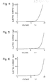
- Figure 4 is graphs illustrating electric characteristics of luminescence elements of this invention, respectively.
- a luminescence element which comprises two electrode layers at least one of which is transparent or translucent and a luminescence function-manifesting layer provided between these two electrode layers, the luminescence function-manifesting layer comprising an inorganic semiconductor thin film layer and an organic semiconductor thin film layer.
- FIG 1 represents a fundamental embodiment of practice of one of them.
- This luminescence element contains two electrode layers 2 and 7, at least one of which is transparent or translucent, and has between these two electrode layers a luminescence function-manifesting layer 6 composed of a laminated layer of an inorganic semiconductor thin film layer 3 and an organic compound thin film layer 4.
- the electrode layer 2 in contact with the inorgamic semiconductor thin film layer 3 is referred to as the first electrode layer
- the electrode layer 7 in contact with the organic compound thin film layer 4 referred to as the second electrode layer.
- the number 1 is a suitable substrate.
- transparent ones are preferred, and examples thereof include plates of glass, quartz, alumina, sapphire, calcium fluoride and the like. If at least the second electrode layer is transparent among the two electrodes, it is also possible to use as substrates opaque ones such as strainless steel sheets and ceramic plates.
- the inorganic semiconductor thin film layer is composed of one kind of an inorganic semiconductor thin film or a laminated film of two or more kinds of inorganic semiconductor thin films.
- the inorganic semiconductor thin film there can be used an amorphous thin film, microcrystalline thin film, polycrystalline thin film, monocrystalline thin film or thin film wherein an amorphous substance and microcrystals are mixed, or a laminate of these thin films, or super lattice thin film, or the like.
- inorganic semiconductor materials include single- element semiconductors such as carbon C, germanium Ge, silicon Si and tin Sn; two-element IV-IV group semiconductors such as SiC and SiGe; III-V group semiconductors such as AlSb, BN, BP, GaN, GaSb, GaAs, GaP, InSb, InAs and InP; II-VI group semiconductor materials such as CdS, CdSe, CdTe, ZnO and ZnS; poly-element compound semiconductor materials; and the like.
- silicon series particularly preferred are those of silicon series, and examples thereof include amorphous Si, hydrogenated amorphous Si, microcrystalline Si, polycrystalline Si, monocrystalline Si, amorphous Si 1-x C x , hydrogenated amorphous Si 1-x C x (a-SiC:H), microcrystalline Si 1-x C x ( ⁇ c-SiC), monocrystalline Si 1-x C x , amorphous Si 1-x N x , hydrogenated amorphous Si 1-x N x , microcrystalline Si 1-x N x , monocrystalline Si 1-x N x , etc.
- the inorganic semiconductor thin film layers those having a p-type or n-type property are preferred.
- the thin film itself may have a p-type or n-type property, or it is also possible to use a thin film converted to p-type or n-type by doping with addition of an impurity giving electroconductivity.
- Thickness of the inorganic semiconductor thin film layer is not particularly limited, but usually preferably on the order of 10 to 3,000 R. It is of course possible to use those having a thickness other than the above.
- various physical or chemical thin film-forming methods such as photo CVD methods, plasma CVD methods, heat CVD methods, molecular beam epitaxy (MBE), organic metal decomposition methods (MOCVD), vapor deposition methods and sputter methods.
- the organic compound thin film layer is composed of one kind of an organic compound thin film or a laminated film of two or more kinds of organic compound thin layers.
- organic compounds there can for example be used suitably organic compounds which have a high luminescence quantum efficiency and j L electron system susceptible to external perturbation and are liable to be easily excited.
- organic compounds there can for example be used condensed polycyclic aromatic hydrocarbons; rubrene; p-terphenyl; 2,5-diphenyloxazole; 1,4-bis-(2-methylstyryl)benzene; xanthine; coumarin; acridine; cyanine dyes; benzophenone; phthalocyanine; and metal complex compounds formed by metal and an organic substance ligand; and compounds forming a complex in an excited state among compounds-heterocyclic compounds other than the above and their derivatives, aromatic amines, aromatic polyamines, and compounds having a quinone structure forming a complex in an excited state; polyacetylene; polysilane; and the like; and mixtures of these compounds.
- metal complex compounds formed by a metal and an organic substance ligand are more specifically explained.
- complex-forming metals Al, Ga, Ir, Zn, Cd, Mg, Pb, Ta, etc. are suitably used, and as organic substance ligands are used porphyrin, chlorophyll, 8-hydroxyquinoline [oxine (Ox)], phthalocyanine, salicylaldehyde oxime, l-nitroso-2-naphthol, cupferron (Nitroso phenyl hydroxylamine Ammonium Salt) dithizone, acetylacetone, etc.
- oxine complexes there can be mentioned oxine complexes, 5,7-dibromooxine complexes (hereinafter represented by diBrOx), 5,7-diiodooxine complexes (hereinafter represented by diIOx), thiooxine complexes (hereinafter represented by ThioOx), seleno- oxine complexes (hereinafter represented by SelOx), methyloxine complexes (hereinafter represented by MeOx), etc.
- diBrOx 5,7-dibromooxine complexes
- diIOx 5,7-diiodooxine complexes
- ThioOx thiooxine complexes
- SelOx seleno- oxine complexes
- MeOx methyloxine complexes
- preferred metal complex compounds include Al(Ox) 3 , Zn(Ox) 2 , Zn(diBrOx) 2 , Zn(diIOx) 2 , Zn(ThioOx) 2 , Zn(SelOx) 2 , Bi(MeOx) 2 , etc.
- Thickness of the organic compound thin film is not particularly limited, but usually on the order of 10 to 5,000 8. It is of course possible to use thickness other than this range.
- various physical or chemical thin film forming methods such as a vacuum vapor deposition method, and further sublimation methods, coating methods (for example, dipping, spin coating, etc.) and the like are also effective.
- the luminescence element of Figure 2 is a thin film type luminescence element, i.e. thin film type EL element characterized in that it has two electrode layers 20 and 70 at least one of which is transparent or translucent and that between these two electrode layers is provided a luminescence function-manifesting layer 60 composed of a laminated layer of a p-type inorganic semiconductor thin film layer 30 and an organic compound thin film layer 40.
- the electrode layer 20 in contact with the inorganic semiconductor thin film layer 30 is referred to as first electrode layer
- the electrode layer 70 in contact with the organic compound thin film layer 40 referred to as second electrode layer.
- the number 10 is a suitable substrate similar to the number 1 in Figure 1.
- first electrode layer 20 and second electrode layer 70 there can be used a thin film of a metal, alloy, metal oxide, metal silicide or the like, or a laminated thin layer of one or two or more kinds of them. More preferably, there can be used materials having a good efficiency of injection of electrons or positive holes into the thin film in contact with the electrode layers.
- an element is further specifically described which is formed by superposing on a transparent or translucent substrate 10 a transparent or translucent first electrode layer 20, a p-type a-SiC:H thin film layer 30 as a p-type inorganic semiconductor thin film layer, a metal complex thin film layer of an organic compound 40 as an organic compound thin film layer, and a second electrode layer 70 in this order.
- the transparent or translucent first electrode layer 20 which comes into contact with the p-type a-SiC:H semiconductor thin film 30 is formed by an electrode material having a good positive hole injection efficiency into the p-type a-SiC:H semiconductor thin film.
- an electrode material having a good positive hole injection efficiency into the p-type a-SiC:H semiconductor thin film.
- Used generally as this electrode material is a thin film of a metal, alloy or metal oxide or the like having a large work function of electron (>4eV), or a laminated thin film of them, or the like.
- the electrode material include thin films of metal oxides such as tin oxide (Sn0 2 ), indium oxide and indium tin oxide (ITO) or their laminted films (for example, ITO/Sn0 2 ), and it is also preferred to use thin films of metals such as Pt, Au, Se, Pd, Ni, W, Ta and Te or alloys or their laminated films, thin films of metal compounds such as CuI or their laminated films, and the like.
- the first electrode layer 20 is shown as a laminated film of the electrode layer 21 and the electrode layer 22.
- the electrode layer 21 is an ITO film and the electrode layer 22 is a Sn0 2 film.
- a metal or alloy thin film or their laminated thin film or the like having a small work function of electron ( ⁇ 4eV) is generally used in order to inject electrons into the metal complex thin film.
- Preferred ones of the electrode layer material include thin films of metals such as Mg, Li, Na, K, Ca, Rb, Sr, Ce and In; thin films of alloys such as Mg-Ag; thin films of alkali metal compounds such as Cs-O-Ag, Cs3Sb, Na 2 KSb and (Cs)Na2KSb ⁇ their laminated thin films; and the like. Thickness of the electrode layer is not particularly limited, but usually on the order of 100 to 10,000 R.
- the EL element can be one formed by superposing on a opaque substrate a first electrode layer, a p-type a-SiC:H thin film layer, a metal complex thin film layer and a transparent or translucent second electrode layer in this order. In case of such an element, luminescence is perceived through the transparent second electrode layer. Further, it is also possible to take out luminescence through the electrodes of both sides by constituting the substrate, first electrode layer and second electrode layer each using a transparent or translucent substance.
- an EL element is formed by superposing on a substrate a second electrode layer, a metal complex thin film layer, a p-type a-SiC:H thin film layer and a first electrode layer in this order.
- EL elements in a structure wherein the EL elements are superposed so as to give a multilayer form, i.e. an electrode layer/a luminescence function-manifesting layer/an electrode layer/a luminescence function-manifesting layer/an electrode layer/a luminescence function-manifesting layer/an electrode layer a luminescence function-manifesting layer/an electrode layer .
- a multilayer element structure By such a multilayer element structure, the adjustment of tone, multiple coloring and the like become possible.
- n-type inorganic semiconductor thin film layer it is preferred to form a two-layer organic compound thin film layer.
- FIG. 3 shows a luminescence element wherein such a n-type thin film is used.
- This luminescence element is a thin film type luminescence element, namely thin film type EL element characterized in that two electrode layers 200 and 700 at least one of which is transparent or translucent are provided, and that between these two electrode layers is provided a luminescence function-manifesting layer 600 comprising a laminated layer of a n-type inorganic semiconductor thin film layer 300, a first organic compound thin film layer 400 and a second organic compound thin film layer 500.
- the organic compound thin film layer composed of the two layers 400 and 500 is a laminate of a layer 400 made of an organic compound which has a high luminescence quantum efficiency and a electron system susceptible to external perturbation and is liable to be easily excited and a layer 500 made of a substance having a large positive hole mobility. More preferably, the organic compound thin film layer is composed of substances transparent to visible radiation.
- organic compound thin film layer 400 there can be used as the organic compound thin film layer 400 the same one as the organic compound thin film layer 40 mentioned above in respect of Figure 2.
- the organic compound thin film layer 500 composed of a substance having a large positive hole mobility is formed on the side of the second electrode layer 700.
- These are, generally, organic compounds containing nitrogen atom(s), a sulfur atom and a phenyl group, and preferred are materials having a drift mobility of 10" cm /V/S or more, under the electric field of at least 10 kV/cm.
- phenylthiophene, phenylpyrrole, et. are mentioned.
- the organic compound thin film can be any of an amorphous thin film, a microcrystalline thin film, an amorphous thin film, an amorphous thin film containing microcrystals, a polycrystalline thin film and a monocrystalline thin film. Thickness of the thin film is not particularly limited, but it is usually suitable that both thickness of the first thin film 400 and that of the second thin film 500 are in the range of 5 to 3,000 g and the thickness in total is 10 to 5,000 g .
- first electrode layer 200 and the second electrode layer 700 can be used as the first electrode layer 200 and the second electrode layer 700 thin film of metals, alloys, metal oxides, metal silicides or the like, or laminated thin films of one or two or more kinds of them, as in the case of the already mentioned. More preferably used are materials having a good efficiency of injection of electrons or positive holes into the thin film in contact with the electrodes.
- an element is further specifically described below which is formed by superposing on a transparent or translucent substrate 100 a transparent or translucent first electrode layer 200, an n-type a-Si:H thin film layer 300 as an inorganic semiconductor thin film layer, a metal complex thin film layer 400 as an organic compound thin film layer, a layer for positive hole transportation 500 and a second electrode layer 700 in this order.
- the first electrode layer 200 which is in contact with the n-Si:H semiconductor thin film 300 and transparent or translucent, is formed from an electrode material having a good efficiency of injection of electrons into the n-type a-Si:H semiconductor thin film.
- This electrode layer is formed from an electrode material which does not form Schottky barrier against the n-type a-Si:H semiconductor thin film, or forms only a small Schottky barrier, if formed.
- the second electrode layer 700 in contact with the organic compound thin film plays a role of injecting positive holes into the organic compound thin film, and thus thin films of metals or alloys having a large work function of electron or their laminated thin films are generally used therefor.
- the EL element can be one formed by superposing on a opaque substrate a first electrode layer, a n-type a-Si:H thin film layer, an organic compound thin film layer and a transparent or translucent second electrode layer in this order. In case of such an element, luminescence is perceived through the transparent second electrode layer. Further, it is also possible to take out luminescence through the electrodes of both sides by constituting the substrate, first electrode layer and second electrode layer each using a transparent or translucent substance.
- an EL element is formed by superposing on a substrate a second electrode layer, a metal complex thin film layer, a n-type a-Si:H thin film layer and a first electrode layer in this order.
- EL elements in a structure wherein the EL elements are superposed so as to give a multilayer form, i.e. an electrode layer/a luminescence function-manifesting layer/an electrode layer/a luminescence function-manifesting layer/an electrode layer/a luminescence function-manifesting layer/an electrode layer a luminescence function-manifesting layer/an electrode layer ....
- a multilayer element structure the adjustment of tone, multiple coloring and the like become possible.
- polymer sheets self- supporting films
- polymer sheets can be used as transparent substrates.
- polymer sheets can be used as transparent substrates.
- polymer sheets include polyethylene terephthalates (PET), polycarbonates (PC), polyethersulfones ( P ES), poly- etheretherketones (PEEK), etc., but polyethylenes (PE), polypropylenes (PP), etc. are also exemplified.
- PET polyethylene terephthalates
- PC polycarbonates
- P ES polyethersulfones
- PEEK poly- etheretherketones
- PE polyethylenes
- PP polypropylenes
- various copolymers as well as homopolymers can be utilized.
- a transparent electroconductive film When a polymer sheet is used as a substrate, it is preferred to form a transparent electroconductive film by providing an electrode layer thereon and then constitute a luminescence element in the same manner as the above using this.
- a transparent electroconductive film By use of such a transparent electroconductive film, it becomes possible to prepare an element having flexibility and it becomes easy to enlarge the area and secure mass productivity thereof.
- transparent electroconductive films are those wherein an oxidation film containing indium as a main component and tin and antimony of the order of 2 to 25 atomic based on the indium as a transparent electroconductive film is formed on a polymer sheet; those wherein a laminated film composed of a composite oxide layer containing indium as a main component and tin or tin and antimony, and a layer of a metal such as gold, silver or palladium or an alloy of them is formed as a transparent electroconductive film on a polymer sheet; etc.
- a transparent electroconductive film (TCO), i.e. first electrode layer 20 was formed on a glass substrate 10 by piling thereon an ITO film 21 to a film thickness of 800 g and further piling thereon an Sn0 2 film 22 to a film thickness of 200 8.
- a p-type inorganic semiconductor thin film layer 30 by piling according to the photo (CVD) method a p-type hydrogenated amorphous silicon carbide film (p-type a-SiC:H) having a film thickness of 50 8, and further piling on this.thin film according to the plasma CVD method a p-type hydrogenated amorphous silicon carbide film (p-type a-SiC:H) having a film thickness of 100 8.
- an organic compound thin film layer 40 was formed on this layer by further piling thereon according to the vacuum resistance heating vapor deposition method a thin film of an aluminum oxine [Al(Ox) 3 ] to a film thickness of 400 8.
- a luminescence function-manifesting layer 60 was formed composed of two layers of the p-type a-SiC:H thin film and the aluminum oxine thin film.
- a second electrode layer 70 was formed on this layer 60 by piling a Mg metal thin film by the electron beam vapor deposition method.
- a luminescence element of this invention as shown in Figure 2 was obtained.
- the area of the vapor deposition film of Mg metal was 3 mm square.
- An element was prepared in the same manner as in Example 1 except that it was formed according to the order of the glass plate/the electrode layer of TCO thin film/the organic compound thin film layer of Al(Ox) 3 thin layer/the electrode layer of Mg metal thin film.
- This element corresponds to the above element from which only the p-type a-SiC:H layer was removed. In case of this element, luminescence was not observed by the naked eye under a usual fluorescent lamp.
- An element was prepared, as a comparative example, in the same manner as in Example 1 except that it was formed according to the order of the glass plate/ the electrode layer of TCO thin film/the organic thin layer/the organic compound thin film layer of Al(Ox) 3 thin film/the electrode layer of Mg metal thin film.
- This element corresponds to an element wherein an organic thin film conducting positive holes is used in place of the p-type a-SiC:H layer.
- As this organic thin film was used one wherein a diamine series derivation compound was processed into thin film by vacuum vapor deposition. In case of this element, both injection current and luminescence intensity were lower than those of the above element by one to two figures. Further, when luminescence was continuously carried out, the lowering of luminescence intensity was observed.
- a transparent first electrode layer 20 was formed on a glass substrate 10 by piling thereon an ITO film 21 to a film thickness of 800 R and further piling thereon an Sno 2 film 22 to a film thickness of 200 R.
- a p-type inorganic semiconductor thin film layer 30 was formed on this first electrode by piling according to the photo CVD method a p-type hydrogenated amorphous silicon carbide film (p-type a-SiC:H) having a film thickness of 50 ⁇ , and further piling on this thin film according to the plasma CVD method a p-type hydrogenated amorphous silicon carbide film (p-type a-SiC:H) having a film thickness of 100 ⁇ .
- an organic compound thin film layer 40 was formed on this layer by further piling thereon according to the vacuum resistance heating vapor deposition method a thin film of rubrene (5,6,11,12-tetraphenylnaphthacene) to a film thickness of 400 ⁇ .
- a luminescence function-manifesting layer 60 was formed composed of two layers of the p-type a-SiC:H thin film and the rubrene thin film.
- a second electrode layer 70 was formed on this layer 60 by piling a Mg metal thin film by the electron beam vapor deposition method.
- an EL element of this invention as shown in Figure 2 was obtained.
- the area of the vapor deposition film of ⁇ g was 3 mm squared.
- Example 2 For comparison, an element was prepared having the same constitution as that of the element in Example 2 except that the p-type a-SiC:H layer was omitted. Volage was impressed on this element in the forward direction, but bright orangish red-colored luminescence, which was observed in Example 2, was not observed under a 30 W-indoor fluorescent lamp.
- An EL element was formed using as a positive hole electroconductive thin film a thin film of a diamine series derivative by vacuum vapor deposition in place of the p-type inorganic semiconductor thin film in Example 2. Namely, this is an EL element composed of the glass substrate/the first electrode/the diamine series derivative organic thin film/rubrene/the second electrode. In case of this element, both injection current and luminescence intensity were lower than those of the above element by one to two figures. Further, in continuous luminescence operation, the lowering of luminescence intensity was observed.
- a luminescence function-manifesting layer of this invention composed of a laminated structure of an inorganic semiconductor thin film layer and an organic compound thin film layer is extremely effective for the enhancement of luminous luminance of EL elements and the improvement of durability of luminescence thereof.
- a transparent first electrode layer 200 was formed on a glass substrate 100 by piling an ITO film 210 to a film thickness of 800 A and then further piling thereon a SnO 2 film 220 to a film thickness of 200 ⁇ .
- On this first electrode was piled a n-type hydrogenated amorphous silicon film 300 ' (n-type a-Si:H) by the plasma CVD method, and on this layer was further piled, first, according to the vacuum resistance heating vapor deposition method an aluminum oxine complex [Al(Ox) 3 ] thin film as a first organic compound thin film layer 400 to a film thickness of 400 ⁇ , and then thereon was piled as a second organic compound thin film layer 500 a positive hole moving layer having a tetraphenylthiophene skeleton to a thickness of 400 ⁇ .
- a luminescence function-manifesting layer 600 was formed composed of the n-type a-Si:H thin film 300 and two layers of the organic compound thin film layers 400 and 500. Then a second electrode layer 700 was formed on this layer 600 by piling thereon a gold thin film according to the resistance heating vapor deposition method. Thus, an EL element of this invention as shown in Figure 3 was obtained.
- the area of the vapor deposition film of gold is 3 mm square.
- Example 3 For comparison, an element was prepared having the same constitution as that of the element in Example 3 except that the n-type a-Si:H layer was omitted. Voltage was impressed on this element in the forward direction, but bright green-colored luminescence, which was observed in Example 3, was not observed under a 30 W-indoor fluorescent lamp.
- an EL element having a sufficient luminous luminance and a stability of the luminous luminance by forming, in an injection EL element which operates by injecting electrons from the one electrode and positive holes from the other electrode, a luminescence function-manifesting layer composed of a two-layer structure of an inorganic semiconductor thin film layer and an organic compound thin film layer between the electrodes.
- such injection luminescence elements of this invention are luminescence elements having high performances which could have not possibly been attained by usual techniques, and industrially extremely useful as thin film light sources, display members or the like.
Landscapes
- Physics & Mathematics (AREA)
- Optics & Photonics (AREA)
- Electroluminescent Light Sources (AREA)
- Led Devices (AREA)
Applications Claiming Priority (7)
| Application Number | Priority Date | Filing Date | Title |
|---|---|---|---|
| JP63292467A JPH02139893A (ja) | 1988-11-21 | 1988-11-21 | 発光素子 |
| JP292467/88 | 1988-11-21 | ||
| JP1013983A JPH02196475A (ja) | 1989-01-25 | 1989-01-25 | 薄膜型発光素子 |
| JP113983/89 | 1989-01-25 | ||
| JP126578/89 | 1989-02-07 | ||
| JP1026578A JPH02207488A (ja) | 1989-02-07 | 1989-02-07 | 薄膜型発光素子 |
| PCT/JP1989/001181 WO1990005998A1 (fr) | 1988-11-21 | 1989-11-21 | Element photo-emetteur |
Publications (3)
| Publication Number | Publication Date |
|---|---|
| EP0397889A1 true EP0397889A1 (de) | 1990-11-22 |
| EP0397889A4 EP0397889A4 (en) | 1991-11-27 |
| EP0397889B1 EP0397889B1 (de) | 1996-02-07 |
Family
ID=27280485
Family Applications (1)
| Application Number | Title | Priority Date | Filing Date |
|---|---|---|---|
| EP89912672A Expired - Lifetime EP0397889B1 (de) | 1988-11-21 | 1989-11-21 | Lichtemittierendes Element |
Country Status (5)
| Country | Link |
|---|---|
| US (1) | US5200668A (de) |
| EP (1) | EP0397889B1 (de) |
| KR (1) | KR950000111B1 (de) |
| DE (1) | DE68925634T2 (de) |
| WO (1) | WO1990005998A1 (de) |
Cited By (5)
| Publication number | Priority date | Publication date | Assignee | Title |
|---|---|---|---|---|
| EP0448268A3 (en) * | 1990-03-13 | 1992-12-02 | Kabushiki Kaisha Toshiba | Semiconductor luminescent device having organic/inorganic junction |
| GB2288062A (en) * | 1994-03-24 | 1995-10-04 | Univ Surrey | Forming luminescent silicon material and devices |
| DE4441973A1 (de) * | 1994-11-25 | 1996-05-30 | Tuhh Tech Gmbh | Lichtwellenleitende Struktur auf einem Substrat |
| WO1996036079A1 (de) * | 1995-05-09 | 1996-11-14 | Robert Bosch Gmbh | Elektrolumineszierendes schichtsystem aus lichtemittierendem organischen material |
| EP0903964A1 (de) * | 1997-09-18 | 1999-03-24 | Eastman Kodak Company | Organische elektrolumineszente Vorrichtung mit inorganischer ladungstransportierender Schicht |
Families Citing this family (48)
| Publication number | Priority date | Publication date | Assignee | Title |
|---|---|---|---|---|
| US5456988A (en) * | 1992-01-31 | 1995-10-10 | Sanyo Electric Co., Ltd. | Organic electroluminescent device having improved durability |
| TW266380B (de) * | 1993-03-29 | 1995-12-21 | Seikosya Kk | |
| JP3199913B2 (ja) * | 1993-06-16 | 2001-08-20 | 株式会社半導体エネルギー研究所 | 液晶電気光学装置およびその作製方法 |
| US5537000A (en) * | 1994-04-29 | 1996-07-16 | The Regents, University Of California | Electroluminescent devices formed using semiconductor nanocrystals as an electron transport media and method of making such electroluminescent devices |
| JPH08102360A (ja) * | 1994-09-29 | 1996-04-16 | Toyota Central Res & Dev Lab Inc | 有機無機複合薄膜型電界発光素子 |
| US5747928A (en) * | 1994-10-07 | 1998-05-05 | Iowa State University Research Foundation, Inc. | Flexible panel display having thin film transistors driving polymer light-emitting diodes |
| JP3529543B2 (ja) * | 1995-04-27 | 2004-05-24 | パイオニア株式会社 | 有機エレクトロルミネッセンス素子 |
| DE19532064A1 (de) * | 1995-08-31 | 1997-03-06 | Bosch Gmbh Robert | Elektrolumineszierendes Schichtsystem |
| US5796120A (en) * | 1995-12-28 | 1998-08-18 | Georgia Tech Research Corporation | Tunnel thin film electroluminescent device |
| US5981092A (en) * | 1996-03-25 | 1999-11-09 | Tdk Corporation | Organic El device |
| JP2000508112A (ja) * | 1996-04-03 | 2000-06-27 | エコール ポリテクニーク フェデラル ドゥ ローザンヌ | エレクトロルミネッセントデバイス |
| US6433355B1 (en) * | 1996-06-05 | 2002-08-13 | International Business Machines Corporation | Non-degenerate wide bandgap semiconductors as injection layers and/or contact electrodes for organic electroluminescent devices |
| DE19625993A1 (de) * | 1996-06-28 | 1998-01-02 | Philips Patentverwaltung | Organisches elektrolumineszentes Bauteil mit Ladungstransportschicht |
| JP3724589B2 (ja) * | 1996-07-29 | 2005-12-07 | ケンブリッジ ディスプレイ テクノロジー リミテッド | エレクトロルミネセンス素子 |
| JPH10162960A (ja) * | 1996-11-27 | 1998-06-19 | Tdk Corp | 有機el発光素子 |
| US5994835A (en) * | 1997-01-13 | 1999-11-30 | Xerox Corporation | Thin film organic light emitting diode with edge emitter waveguide and electron injection layer |
| US5958573A (en) * | 1997-02-10 | 1999-09-28 | Quantum Energy Technologies | Electroluminescent device having a structured particle electron conductor |
| US6607829B1 (en) * | 1997-11-13 | 2003-08-19 | Massachusetts Institute Of Technology | Tellurium-containing nanocrystalline materials |
| US6207392B1 (en) * | 1997-11-25 | 2001-03-27 | The Regents Of The University Of California | Semiconductor nanocrystal probes for biological applications and process for making and using such probes |
| WO2000001203A1 (en) * | 1998-06-26 | 2000-01-06 | Idemitsu Kosan Co., Ltd. | Luminescent device |
| JP4673947B2 (ja) * | 1999-02-15 | 2011-04-20 | 出光興産株式会社 | 有機エレクトロルミネッセンス素子およびその製造方法 |
| JP2001217456A (ja) * | 2000-02-03 | 2001-08-10 | Sharp Corp | 窒化ガリウム系化合物半導体発光素子 |
| JP4112800B2 (ja) * | 2000-12-05 | 2008-07-02 | 富士フイルム株式会社 | 発光素子及びその製造方法 |
| DE10234977A1 (de) | 2002-07-31 | 2004-02-12 | Osram Opto Semiconductors Gmbh | Strahlungsemittierendes Dünnschicht-Halbleiterbauelement auf GaN-Basis |
| EP1388903B1 (de) * | 2002-08-09 | 2016-03-16 | Semiconductor Energy Laboratory Co., Ltd. | Organische elektrolumineszente Vorrichtung |
| JP4185097B2 (ja) | 2003-03-13 | 2008-11-19 | 出光興産株式会社 | 新規含窒素複素環誘導体及びそれを用いた有機エレクトロルミネッセンス素子 |
| JP2005075868A (ja) * | 2003-08-29 | 2005-03-24 | Fujitsu Ltd | 蛍光材料、有機エレクトロルミネッセンス素子および有機エレクトロルミネッセンスディスプレイ |
| JP4131218B2 (ja) * | 2003-09-17 | 2008-08-13 | セイコーエプソン株式会社 | 表示パネル、及び表示装置 |
| EP1665398B1 (de) * | 2003-09-26 | 2014-07-02 | OSRAM Opto Semiconductors GmbH | Strahlungsemittierender dünnschicht-halbleiterchip |
| KR100682870B1 (ko) * | 2004-10-29 | 2007-02-15 | 삼성전기주식회사 | 다층전극 및 이를 구비하는 화합물 반도체 발광소자 |
| US20090015150A1 (en) * | 2005-07-15 | 2009-01-15 | Lg Chem, Ltd. | Organic light emitting device and method for manufacturing the same |
| TWI321968B (en) * | 2005-07-15 | 2010-03-11 | Lg Chemical Ltd | Organic light meitting device and method for manufacturing the same |
| KR20080042887A (ko) * | 2005-09-12 | 2008-05-15 | 이데미쓰 고산 가부시키가이샤 | 도전성 적층체 및 유기 el 소자 |
| US8835941B2 (en) * | 2006-02-09 | 2014-09-16 | Qd Vision, Inc. | Displays including semiconductor nanocrystals and methods of making same |
| WO2007095061A2 (en) * | 2006-02-09 | 2007-08-23 | Qd Vision, Inc. | Device including semiconductor nanocrystals and a layer including a doped organic material and methods |
| WO2007143197A2 (en) * | 2006-06-02 | 2007-12-13 | Qd Vision, Inc. | Light-emitting devices and displays with improved performance |
| JP2010508620A (ja) * | 2006-09-12 | 2010-03-18 | キユーデイー・ビジヨン・インコーポレーテツド | 所定のパターンを表示するために有用なエレクトロルミネセントディスプレイ |
| JP5465825B2 (ja) * | 2007-03-26 | 2014-04-09 | 出光興産株式会社 | 半導体装置、半導体装置の製造方法及び表示装置 |
| US8330149B2 (en) * | 2007-09-28 | 2012-12-11 | The Johns Hopkins University | Megahertz organic/polymer diodes |
| EP2223357B1 (de) * | 2007-12-14 | 2016-08-10 | Philips Intellectual Property & Standards GmbH | Organische lichtemittierende vorrichtung mit einstellbarer ladungsträgerinjektion |
| US9525148B2 (en) | 2008-04-03 | 2016-12-20 | Qd Vision, Inc. | Device including quantum dots |
| KR101995369B1 (ko) | 2008-04-03 | 2019-07-02 | 삼성 리서치 아메리카 인코포레이티드 | 양자점들을 포함하는 발광 소자 |
| WO2010122782A1 (ja) * | 2009-04-24 | 2010-10-28 | パナソニック株式会社 | 有機elディスプレイおよびその製造方法 |
| KR101723540B1 (ko) * | 2010-07-30 | 2017-04-05 | 엘지이노텍 주식회사 | 발광 소자 및 이를 갖는 발광 소자 패키지 |
| JP6041336B2 (ja) * | 2012-02-15 | 2016-12-07 | 国立大学法人山形大学 | 有機エレクトロルミネッセンス素子 |
| JP6108355B2 (ja) * | 2012-02-15 | 2017-04-05 | 国立大学法人山形大学 | 有機エレクトロルミネッセンス素子 |
| KR102323243B1 (ko) * | 2015-07-22 | 2021-11-08 | 삼성디스플레이 주식회사 | 유기 발광 소자 및 이를 포함하는 유기 발광 표시 장치 |
| KR200485202Y1 (ko) * | 2016-02-12 | 2017-12-07 | 김영준 | 화재 사전 진압 구조의 청소기 |
Family Cites Families (6)
| Publication number | Priority date | Publication date | Assignee | Title |
|---|---|---|---|---|
| GB1572181A (en) * | 1975-08-18 | 1980-07-23 | Ici Ltd | Device comprising a thin film of organic materila |
| US4539507A (en) * | 1983-03-25 | 1985-09-03 | Eastman Kodak Company | Organic electroluminescent devices having improved power conversion efficiencies |
| JP2540673B2 (ja) * | 1991-07-10 | 1996-10-09 | 株式会社テンリュウテクニックス | トレイおよび電子部品の供給装置 |
| JPH06155184A (ja) * | 1992-11-30 | 1994-06-03 | Nippon Steel Corp | 自動嵌合装置 |
| JP2857561B2 (ja) * | 1993-02-22 | 1999-02-17 | 旭化成電子株式会社 | ペリクル |
| JPH06276576A (ja) * | 1993-03-22 | 1994-09-30 | Fujitsu Ten Ltd | 機器制御システム |
-
1989
- 1989-11-21 KR KR1019900701577A patent/KR950000111B1/ko not_active Expired - Fee Related
- 1989-11-21 US US07/536,567 patent/US5200668A/en not_active Expired - Lifetime
- 1989-11-21 EP EP89912672A patent/EP0397889B1/de not_active Expired - Lifetime
- 1989-11-21 WO PCT/JP1989/001181 patent/WO1990005998A1/ja not_active Ceased
- 1989-11-21 DE DE68925634T patent/DE68925634T2/de not_active Expired - Fee Related
Cited By (7)
| Publication number | Priority date | Publication date | Assignee | Title |
|---|---|---|---|---|
| EP0448268A3 (en) * | 1990-03-13 | 1992-12-02 | Kabushiki Kaisha Toshiba | Semiconductor luminescent device having organic/inorganic junction |
| GB2288062A (en) * | 1994-03-24 | 1995-10-04 | Univ Surrey | Forming luminescent silicon material and devices |
| US5852346A (en) * | 1994-03-24 | 1998-12-22 | University Of Surrey | Forming luminescent silicon material and electro-luminescent device containing that material |
| DE4441973A1 (de) * | 1994-11-25 | 1996-05-30 | Tuhh Tech Gmbh | Lichtwellenleitende Struktur auf einem Substrat |
| DE4441973C2 (de) * | 1994-11-25 | 2000-01-05 | Tuhh Tech Gmbh | Lichtwellenleitende Struktur auf einem Substrat |
| WO1996036079A1 (de) * | 1995-05-09 | 1996-11-14 | Robert Bosch Gmbh | Elektrolumineszierendes schichtsystem aus lichtemittierendem organischen material |
| EP0903964A1 (de) * | 1997-09-18 | 1999-03-24 | Eastman Kodak Company | Organische elektrolumineszente Vorrichtung mit inorganischer ladungstransportierender Schicht |
Also Published As
| Publication number | Publication date |
|---|---|
| DE68925634D1 (de) | 1996-03-21 |
| DE68925634T2 (de) | 1996-08-22 |
| KR950000111B1 (ko) | 1995-01-09 |
| EP0397889B1 (de) | 1996-02-07 |
| WO1990005998A1 (fr) | 1990-05-31 |
| US5200668A (en) | 1993-04-06 |
| EP0397889A4 (en) | 1991-11-27 |
| KR900702580A (ko) | 1990-12-07 |
Similar Documents
| Publication | Publication Date | Title |
|---|---|---|
| US5200668A (en) | Luminescence element | |
| US5128587A (en) | Electroluminescent device based on organometallic membrane | |
| US5117267A (en) | Semiconductor heterojunction structure | |
| JP3237905B2 (ja) | 有機el素子 | |
| JPH0268968A (ja) | 化合物半導体発光素子 | |
| CN111540837B (zh) | 量子点发光器件和显示装置 | |
| JP2788531B2 (ja) | 有機錯体発光素子 | |
| WO2022105626A1 (zh) | 量子点发光二极管、显示装置和发光光源 | |
| Boonkosum et al. | Amorphous visible-light thin film light-emitting diode having a-SiN: H as a luminescent layer | |
| JPH02196475A (ja) | 薄膜型発光素子 | |
| Chichibu et al. | Fabrication of p-CuGaS2/n-ZnO: Al heterojunction light-emitting diode grown by metalorganic vapor phase epitaxy and helicon-wave-excited-plasma sputtering methods | |
| JPH02207488A (ja) | 薄膜型発光素子 | |
| JPH02139893A (ja) | 発光素子 | |
| JPH02253593A (ja) | 発光素子 | |
| JP2837223B2 (ja) | 有機発光素子 | |
| Przezdziecka et al. | Current transport mechanisms in zinc oxide/silicon carbide heterojunction light‐emitting diodes | |
| CA2036497A1 (en) | Luminescence element | |
| JP2837171B2 (ja) | 透明導電性フィルム | |
| JP3102867B2 (ja) | 発光素子 | |
| JP3137631B2 (ja) | 発光素子 | |
| Gordon | Electroluminescence by impact excitation in ZnS: Mn and ZnSe: Mn Schottky diodes | |
| JP2971482B2 (ja) | エレクトロクロミック素子 | |
| Yamamoto et al. | Preparation and Electroluminescent Properties of p-n Junctions in Cd1-x Mg x Te | |
| JP3541690B2 (ja) | 発光素子の製造方法 | |
| JP2597624B2 (ja) | 半導体発光素子 |
Legal Events
| Date | Code | Title | Description |
|---|---|---|---|
| PUAI | Public reference made under article 153(3) epc to a published international application that has entered the european phase |
Free format text: ORIGINAL CODE: 0009012 |
|
| AK | Designated contracting states |
Kind code of ref document: A1 Designated state(s): DE FR GB IT NL |
|
| 17P | Request for examination filed |
Effective date: 19900811 |
|
| A4 | Supplementary search report drawn up and despatched |
Effective date: 19911007 |
|
| AK | Designated contracting states |
Kind code of ref document: A4 Designated state(s): DE FR GB IT NL |
|
| 17Q | First examination report despatched |
Effective date: 19930525 |
|
| RBV | Designated contracting states (corrected) |
Designated state(s): DE GB NL |
|
| GRAA | (expected) grant |
Free format text: ORIGINAL CODE: 0009210 |
|
| AK | Designated contracting states |
Kind code of ref document: B1 Designated state(s): DE GB NL |
|
| PG25 | Lapsed in a contracting state [announced via postgrant information from national office to epo] |
Ref country code: NL Free format text: LAPSE BECAUSE OF FAILURE TO SUBMIT A TRANSLATION OF THE DESCRIPTION OR TO PAY THE FEE WITHIN THE PRESCRIBED TIME-LIMIT Effective date: 19960207 |
|
| REF | Corresponds to: |
Ref document number: 68925634 Country of ref document: DE Date of ref document: 19960321 |
|
| NLV1 | Nl: lapsed or annulled due to failure to fulfill the requirements of art. 29p and 29m of the patents act | ||
| PLBE | No opposition filed within time limit |
Free format text: ORIGINAL CODE: 0009261 |
|
| STAA | Information on the status of an ep patent application or granted ep patent |
Free format text: STATUS: NO OPPOSITION FILED WITHIN TIME LIMIT |
|
| 26N | No opposition filed | ||
| REG | Reference to a national code |
Ref country code: GB Ref legal event code: 732E |
|
| REG | Reference to a national code |
Ref country code: GB Ref legal event code: IF02 |
|
| PGFP | Annual fee paid to national office [announced via postgrant information from national office to epo] |
Ref country code: GB Payment date: 20061115 Year of fee payment: 18 |
|
| PGFP | Annual fee paid to national office [announced via postgrant information from national office to epo] |
Ref country code: DE Payment date: 20061116 Year of fee payment: 18 |
|
| GBPC | Gb: european patent ceased through non-payment of renewal fee |
Effective date: 20071121 |
|
| PG25 | Lapsed in a contracting state [announced via postgrant information from national office to epo] |
Ref country code: DE Free format text: LAPSE BECAUSE OF NON-PAYMENT OF DUE FEES Effective date: 20080603 |
|
| PG25 | Lapsed in a contracting state [announced via postgrant information from national office to epo] |
Ref country code: GB Free format text: LAPSE BECAUSE OF NON-PAYMENT OF DUE FEES Effective date: 20071121 |