EP0398189A2 - Direktzugriffsspeicher zur Angabe von nichtcachespeicherbaren Adressen - Google Patents
Direktzugriffsspeicher zur Angabe von nichtcachespeicherbaren Adressen Download PDFInfo
- Publication number
- EP0398189A2 EP0398189A2 EP90108940A EP90108940A EP0398189A2 EP 0398189 A2 EP0398189 A2 EP 0398189A2 EP 90108940 A EP90108940 A EP 90108940A EP 90108940 A EP90108940 A EP 90108940A EP 0398189 A2 EP0398189 A2 EP 0398189A2
- Authority
- EP
- European Patent Office
- Prior art keywords
- storing
- computer system
- random access
- memory
- value
- Prior art date
- Legal status (The legal status is an assumption and is not a legal conclusion. Google has not performed a legal analysis and makes no representation as to the accuracy of the status listed.)
- Granted
Links
Images


Classifications
-
- G—PHYSICS
- G06—COMPUTING OR CALCULATING; COUNTING
- G06F—ELECTRIC DIGITAL DATA PROCESSING
- G06F12/00—Accessing, addressing or allocating within memory systems or architectures
- G06F12/02—Addressing or allocation; Relocation
- G06F12/08—Addressing or allocation; Relocation in hierarchically structured memory systems, e.g. virtual memory systems
- G06F12/0802—Addressing of a memory level in which the access to the desired data or data block requires associative addressing means, e.g. caches
- G06F12/0888—Addressing of a memory level in which the access to the desired data or data block requires associative addressing means, e.g. caches using selective caching, e.g. bypass
-
- G—PHYSICS
- G06—COMPUTING OR CALCULATING; COUNTING
- G06F—ELECTRIC DIGITAL DATA PROCESSING
- G06F12/00—Accessing, addressing or allocating within memory systems or architectures
- G06F12/02—Addressing or allocation; Relocation
- G06F12/08—Addressing or allocation; Relocation in hierarchically structured memory systems, e.g. virtual memory systems
Definitions
- the invention relates to computer systems utilizing cache memory systems, and more particularly to computer systems where certain ranges of main memory address are not cacheable.
- personal computer systems are flexible units which can be configured in many different ways.
- personal computers compatible with personal computers developed by International Business Machines Corp. can have memory logically located in varying locations, depending on the specific design.
- IBM International Business Machines Corp.
- certain portions of the memory have not been cacheable because devices share the memory, such as video display systems, the memory is read only (ROM), or the location is not readable and writable, such as device control registers.
- ROM read only
- writable such as device control registers.
- certain locations in the memory map must be indicated as noncacheable to any controller handling the cache system.
- PAL programmable array logic
- a computer system utilizes random access memory (RAM) to perform the decoding function for noncacheable addresses.
- the RAM is connected with its address inputs connected to the address bus and with a data output coupled to the cache controller's noncacheable address input.
- the RAM outputs a value indicative of the cacheability of that memory block. Because a RAM is being utilized each memory block can be individually programmed to a proper condition, thus removing the restrictions of the PAL and allowing small users or special applications to have a correctly configured cacheability map.
- the RAM is initially loaded during power on self test (POST) operations and can be read or modified at other times.
- Writing to the RAM is accomplished by setting the desired data value, a write flag and a programming value by performing an input/output (I/O) write operation to an I/O port associated with the circuitry of the present invention.
- the I/O port is read to insure that the I/O write operation is complete.
- a memory write operation to the desired memory block completes the sequence.
- the memory write operation is done in a local bus access mode so that the main memory of the system is not affected. This process is repeated for all the memory blocks to insure that the proper values are present in the RAM.
- Reading the RAM is accomplished by setting a read flag and the program value by performing an I/O write.
- An I/O read operation is performed to verify the request and a local bus memory write operation to the desired block is performed.
- the RAM data value is latched into a flip-flop during the memory write operation, the data value can be read by performing an I/O port read operation.
- the present invention allows improved flexibility in a computer system using a memory cache of the cacheability of a given memory block.
- the letter P generally represents a microprocessor
- the letter M generally represents cache memory
- the letter C generally represents a cache controller in a computer system incorporating the present invention.
- the microprocessor P is an Intel Corporation 80386-33 and the cache controller C is an Intel Corporation 82385-33, for reasons which will be explained.
- the microprocessor P, the cache memory M and the cache controller C are connected in a conventional manner with the resulting formation of local data, address and control busses L. These local busses L are interfaced to the remaining portions of the computer system, including main memory 11, by a series of buffers and transceivers 10.
- the cache controller C has two inputs of particular interest in this invention.
- the first input is the LBA* input or local bus access input.
- the cache controller C acknowledges that the operation which is being requested by the microprocessor P is being directed to a device on the local bus L and not to portions of the computer system coupled by the buffers and transceivers 10.
- the cache controller C does not control operation of the various devices and is essentially idle.
- the other input of interest is the NCA* or noncacheable address input.
- the cache controller C understands that this particular memory address is not cacheable and therefore passes the operation on through to the memory devices external to the local bus L without affecting the cache memory M.
- the LBA* signal is generated by a noncacheable address (NCA) programmable array logic (PAL) device 12.
- NCA PAL 12 utilizes the LW-R signal, the LM-IO signal and the PGM signal to determine the LBA* signal.
- the LW-R signal is the write or read indication signal present on the local control bus and the LM-IO signal is the memory space or I/O space indication signal present on the local bus L as developed by the processor P.
- the PGM signal is the signal which is present to indicate that programming of an NCA random access memory (RAM) 14 is desired.
- the LBA* signal is made low to indicate to the cache controller C that a local bus operation is being performed. This condition is provided so that the memory write operation does not affect the memory of the computer system but is instead directed only to the NCA RAM 14.
- the NCA RAM 14 is used to store the data values indicating whether a given block of memory is cacheable or noncacheable. To this end, the NCA RAM 14 has its address inputs connected to various address lines in the local address bus, for example, lines ⁇ 13-23,31>.
- the data port 16 of the NCA RAM 14 is connected to the NCA* input of the cache controller C through an optional resistor 18.
- the resistor 18 is preferably a zero value resistor which can effectively be utilized for jumpering purposes during manufacture. Because the NCA RAM 14 is always enabled, whenever an address is present on the local bus L, the NCA RAM 14 is providing a signal to the NCA* input of the cache controller C, except during write operations to the NCA RAM 14.
- the data port 16 of the NCA RAM 14 is also connected to the output of a tristate buffer 20 and the D input of a D-type flip-flop 22.
- the buffer 20 and the flip-flop 22 are used to interface the data port 16 of the NCA RAM 14 with the processor P to allow programming of the NCA RAM 14 or reading of value stored in the NCA RAM 14.
- the NCA RAM 14 is preferably a very fast static RAM, such as a 15 nanosecond RAM. This high speed is necessary because of the high speed operation of the microprocessor P and the cache controller C and of the timing requirements between the presentation of the address values on the local bus L and the need for the NCA* signal to be valid to the cache controller C. This is possible utilizing an NCA RAM 14 of the speed indicated when utilizing the preferred 80386-33 microprocessor P and the preferred 82385-33 cache controller C. For example, had the 20 MHz version of the above-referenced units been utilized, this invention would not be possible with RAM's which are readily available at this time.
- the 82385-20 requires that the NCA* signal be valid 10 nanoseconds prior to the beginning of a PHI1 of the CLK2 signal.
- the 80386-20 cannot guarantee that at a 20 MHz clock rate the address information is present until 20 nanoseconds prior to this same edge of CLK2. Therefore, this leaves only 10 nanoseconds from guaranteed address valid to the time the NCA* signal must be valid. This cannot be done with available RAM memories of sufficient size and therefore the PAL version had to be previously utilized.
- the timings have been changed so that the NCA* signal must be valid 13 nanoseconds prior to the PHI2 portion of the CLK2 signal cycle in the CLK2 signal cycle following the addresses becoming valid on the 80386-33.
- the 80386-33 worst case presentation of the address value is 30 nanoseconds prior to this edge, therefore leaving a worst case timing of 17 nanoseconds between the known validity of the address data and the need for the NCA* signal to be valid.
- a 15 nanosecond NCA RAM 14 as utilized in the preferred embodiment is capable of performing the necessary operations.
- NCA RAM 14 is a random access memory, when it is initially powered up, random and possibly improper values are stored in the NCA RAM 14. Therefore, it is necessary to write desired values into the NCA RAM 14. This is accomplished by the use of several registers and certain gates.
- An input/output (I/O) port designated as C67 in the computer system of the preferred embodiment is assigned to have certain bits relating to programming, that is reading or writing, the NCA RAM 14. Three bits in I/O port C67 are utilized in programming the NCA RAM 14. The three bits are designated the PGM bit, the NCAW-R bit and the NCAD* bit. The NCAD* bit is actually two different bits, NCADI* for input or write purposes and NCADO* for output or read purposes.
- the PGM bit is stored in a D-type flip-flop 24 (Fig. 2).
- Bit 7 of the system data bus 25 is connected to the D input, with the clock input being the inverted version of a WRC67 signal.
- the WRC67 signal is a signal which goes high when a valid write operation is being performed to I/O port 67, with the timing such that the data is valid prior to the falling edge of the WRC67 signal.
- the rising edge of the clock signal provided to the PGM flip-flop 24 is of such a phase and sequence that the data is present on the system data bus 25 and is latched into the PGM flip-flop 24.
- the noninverting output of the PGM flip-flop 24 provides the PGM signal.
- the NCAW-R and NCADI* bits that is the noncacheable address write and noncacheable address data input bits, are stored by a latch 26.
- Bits 6 and 5, respectively, of the system data bus 25 are connected to the latch 26, with the WRC67 signal connected to the enable input of the latch 26.
- the timing of the WRC67 signal is such that the data is present and latched into the latch 26 where the WRC signal goes low.
- the outputs of the latch 26 corresponding to the NCAW-R and NCADI* bits produce the NCAW-R and NCADI* signals.
- the utilization of the signals is as follows: the PGM signal is utilized to indicate that the programming mode of the NCA RAM is desired.
- the NCAW-R signal is utilized to indicate whether the NCA RAM 14 will have data values written to it or read from it.
- the NCADI* signal is used as the input path to the NCA RAM 14 and is connected to the input of the buffer 20.
- the PGM, NCAW-R signals and a signal referred to as the NCADO* signal, the output of the flip-flop 22, are connected as inputs to a buffer 28.
- the buffer 28 is used to control the presentation of these three signals onto the system data bus 25 at bit positions ⁇ 7-5>.
- the output control of the buffer 28 is based on a signal referred to as RDC67, which has timing such that it is valid low when a read request to I/O port C67 is being presented by the processor P.
- the NCADI* signal is presented to the input of buffer 20 whose output is connected to the data port 16 of the NCA RAM 14.
- the NCADI* signal value is latched into the NCA RAM 14 when the output of a three input NAND gate 30 (Fig. 1) goes high.
- the output of the NAND gate 30 is connected to the write enable input of the NCA RAM 14.
- the three inputs to the NAND gate 30 are the PGM and NCAW-R signals and a signal referred to as PGMACT.
- the PGMACT signal is a signal that indicates that programming mode is active, that a memory operation is being performed, that the memory operation is a write operation and that it is an appropriate time to latch data into the NCA RAM 14 or to present data to the flip-flop 22.
- the next memory write operation produces a write pulse out of the NAND gate 30.
- the output of the NAND gate 30 is also connected to the buffer control input of the NCADI* buffer 20, so that when the output of the NAND gate 30 is low, the data value which is present at the buffer 20, that is the NCADI* value, is transmitted to the data port 16 for storage in the NCA RAM 14 at the location determined by the address of the memory write operation.
- the PGMACT signal has a width such that the data is presented to the NCA RAM 14 for an adequate period of time.
- the data which is present at the NCADI* signal is stored in the address given by the memory write operation which has been requested by the processor P. Therefore, by properly sequencing through blocks of the address and repeating the programming and data value positioning in the register and latch 26, the NCA RAM 14 can properly be loaded with desired data values.
- a signal referred to as PGMCLR* is connected to the clear input of the PGM flip-flop 24.
- the PGMCLR* signal is such that it goes low for a short period after the PGMACT signal is no longer true.
- the PGM flip-flop 24 is cleared so that should further memory write operations occur, the contents of the NCA RAM 14 at the memory address are not accidentally changed to undesired values.
- Reading data from the NCA RAM 16 utilizes the flip-flop 22.
- a NAND gate 32 is utilized to clock the data present at the output of the data port 16 of the NCA RAM 14 into the flip-flop 22.
- the output of the NAND gate 32 is connected to the clocking input of flip-flop 22 and the NAND gate 32 has three inputs.
- the three inputs are the PGM signal, the PGMACT signal and the inversion of the NCAW-R signal.
- the processor P can then read the I/O port C67 to obtain the particular noncacheable value which is stored in the RAM 14 at the memory block which had been addressed in the memory write operation.
- the automatic clearing of PGM flip-flop 24 by the PGMCLR* signal prevents the accidental reading of an undesired noncacheable value.
- the NCA PAL 12 there is an output from the NCA PAL 12 called the PALNCA* signal.
- This signal is connected through a resistor 40 to the NCA* input of the cache controller C.
- the resistor 18 or 40 of the non-desired mode of presenting the NCA* signal to the cache controller C is removed so that a connection is actually not present and thus there is no interference between the two signals as developed by the NCA PAL 12 and the NCA RAM 14.
- the memory write operations which are utilized to read from or write to the NCA RAM 14 are being performed in local bus mode as determined by the NCA PAL 14. Thus, the write operations do not affect other memory which can be present in the system on other than the local bus.
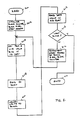
- FIG. 3 shows a write sequence 100 utilized with circuitry as indicated in Figs. 1 and 2 for writing values to the NCA RAM 14.
- various values are initialized. These values include a counter which is to count the number of memory blocks which are to be programmed, the memory block size and the starting address of the memory blocks to be programmed.
- Control proceeds to step 104, where the processor P writes to I/O port C67, setting the PGM and NCAW-R signals high and setting the NCADI* signal as desired for that particular memory block.
- the processor P reads I/O port C67. This read operation is necessary because the cache controller C posts write operations and therefore the I/O port write operation may not be completed before the local bus memory write operation which sets the NCA RAM 14 value.
- This I/O read operation forces the I/O write operation to be completed, so that the values are properly stored in I/O port C67.
- Control proceeds to step 110, where a memory write operation to the memory block as indicated by the start address value is performed. This memory write operation thus automatically loads the value which had been written to the NCADI* bit into the NCA RAM 14 at the location as identified by the address lines connected to the NCA RAM 14.
- Control proceeds to step 112, where a determination is made as to whether the last memory block necessary has been programmed into the NCA RAM 14. If not, control proceeds to step 114, where the starting address is incremented by the block size and the memory block counter is incremented. Control then proceeds to state 104 to continue the sequence of programming the NCA RAM 14.
- step 112 If it was determined in step 112 that the last block of memory had been programmed, then control proceeds to step 116 which is the end of the write sequence 100, with control generally being passed to other portions of the power on self test (POST) routine utilized in a computer system.
- POST power on self test
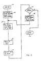
- An exemplary read sequence 200 utilized to read the noncacheable values of a series of blocks starts at step 202 (Fig. 4).
- step 202 a number of values such as the block counter, the block size and the starting memory address are initialized as desired.
- Control proceeds to step 204, where I/O port C67 is written, setting the PGM value high and the W-R value low to indicate programming mode operation and a read operation to be performed.
- step 208 the processor P reads I/O port C67 for reasons indicated above.
- Control proceeds from step 208 to step 210, where a memory write operation is performed to the memory block as indicated by the starting address. This memory write operation causes the data value which is present in the NCA RAM 14 to be latched into the flip-flop 22.
- the processor P then reads I/O port C67 in step 212.
- the value returned at bit 5 of the data word is the NCAD0* signal, which allows the processor P to determine the noncacheable data value which is present in the NCA RAM 14 at the location of the memory block which was present in the memory write operation of step 210.
- Control proceeds to step 214, where a determination is made if this was the last block which is desired to be read. If not, control proceeds to step 216, where the starting address is incremented by the block size and the block counter is incremented as needed. Control proceeds to step 204 and the operation is performed again. If this was the last block, control proceeds from step 214 to step 216, which is the end of the sequence 200, and to the next operation which is to be performed by the computer system.
- NCA RAM 14 is preferably a conventional random access memory, it can also be an electrically erasable programmable read only memory (EEPROM) or similar memory having a sufficiently fast access time. If an EEPROM is utilized the write operation is not necessary on system power up after the initial programming, but is changed only when map changes are desired.
- EEPROM electrically erasable programmable read only memory
- this technique allows the development of a very flexible system for determining the characteristics of a given memory block, for example, when a given memory address block is noncacheable, so that individual users can adjust the characteristic map of their individual computer system if desired.
Landscapes
- Engineering & Computer Science (AREA)
- Theoretical Computer Science (AREA)
- Physics & Mathematics (AREA)
- General Engineering & Computer Science (AREA)
- General Physics & Mathematics (AREA)
- Memory System Of A Hierarchy Structure (AREA)
- Multi Processors (AREA)
Applications Claiming Priority (2)
| Application Number | Priority Date | Filing Date | Title |
|---|---|---|---|
| US07/354,513 US5210847A (en) | 1989-05-19 | 1989-05-19 | Noncacheable address random access memory |
| US354513 | 1989-05-19 |
Publications (3)
| Publication Number | Publication Date |
|---|---|
| EP0398189A2 true EP0398189A2 (de) | 1990-11-22 |
| EP0398189A3 EP0398189A3 (de) | 1991-10-23 |
| EP0398189B1 EP0398189B1 (de) | 1997-03-05 |
Family
ID=23393673
Family Applications (1)
| Application Number | Title | Priority Date | Filing Date |
|---|---|---|---|
| EP90108940A Expired - Lifetime EP0398189B1 (de) | 1989-05-19 | 1990-05-11 | Direktzugriffsspeicher zur Angabe von nichtcachespeicherbaren Adressen |
Country Status (6)
| Country | Link |
|---|---|
| US (1) | US5210847A (de) |
| EP (1) | EP0398189B1 (de) |
| JP (1) | JPH0395650A (de) |
| KR (1) | KR900018820A (de) |
| CA (1) | CA2016544A1 (de) |
| DE (1) | DE69030022D1 (de) |
Cited By (3)
| Publication number | Priority date | Publication date | Assignee | Title |
|---|---|---|---|---|
| EP0509676A1 (de) * | 1991-04-15 | 1992-10-21 | International Business Machines Corporation | Cache-Speichersteuerungsanordnung |
| EP0525308A1 (de) * | 1991-07-31 | 1993-02-03 | International Business Machines Corporation | Speicherabbildung für einen Prozessor-Cache-Speicher |
| EP1126375A1 (de) * | 2000-02-18 | 2001-08-22 | Texas Instruments Incorporated | Cache-Speicher der von System-Adresseigenschaften gesteuert wird |
Families Citing this family (13)
| Publication number | Priority date | Publication date | Assignee | Title |
|---|---|---|---|---|
| US6009495A (en) * | 1989-12-29 | 1999-12-28 | Packard Bell Nec | Protected address range in an electrically erasable programmable read only memory |
| EP0809185B1 (de) * | 1990-09-18 | 1999-12-08 | Fujitsu Limited | Verfahren zur Vervielfältigung eines geteilten Speichers |
| US5319767A (en) * | 1992-06-29 | 1994-06-07 | The United States Of America As Represented By The Secretary Of The Navy | Slave controller for effecting a block transfer of sixteen bit words between a memory and a data transfer bus |
| US5678025A (en) * | 1992-12-30 | 1997-10-14 | Intel Corporation | Cache coherency maintenance of non-cache supporting buses |
| US5572700A (en) * | 1993-04-30 | 1996-11-05 | Intel Corporation | Cache access controller and method for permitting caching of information in selected cache lines |
| US5893154A (en) * | 1993-07-06 | 1999-04-06 | Intel Corporation | CPU write-back cache coherency mechanism that transeers data from a cache memory to a main memory before access of the main memory by an alternate bus master |
| US5551006A (en) * | 1993-09-30 | 1996-08-27 | Intel Corporation | Low cost writethrough cache coherency apparatus and method for computer systems without a cache supporting bus |
| US5890216A (en) * | 1995-04-21 | 1999-03-30 | International Business Machines Corporation | Apparatus and method for decreasing the access time to non-cacheable address space in a computer system |
| US6044441A (en) * | 1995-09-29 | 2000-03-28 | Intel Corporation | Method and apparatus for encoding valid and invalid states in a cache with an invalid pattern |
| US5951657A (en) * | 1996-06-19 | 1999-09-14 | Wisconsin Alumni Research Foundation | Cacheable interface control registers for high speed data transfer |
| US6021470A (en) * | 1997-03-17 | 2000-02-01 | Oracle Corporation | Method and apparatus for selective data caching implemented with noncacheable and cacheable data for improved cache performance in a computer networking system |
| US6564299B1 (en) * | 2001-07-30 | 2003-05-13 | Lsi Logic Corporation | Method and apparatus for defining cacheable address ranges |
| US20090089515A1 (en) * | 2007-10-02 | 2009-04-02 | Qualcomm Incorporated | Memory Controller for Performing Memory Block Initialization and Copy |
Family Cites Families (11)
| Publication number | Priority date | Publication date | Assignee | Title |
|---|---|---|---|---|
| US4665506A (en) * | 1983-01-03 | 1987-05-12 | Texas Instruments Incorporated | Memory system with write protection |
| US4622631B1 (en) * | 1983-12-30 | 1996-04-09 | Recognition Int Inc | Data processing system having a data coherence solution |
| US4669043A (en) * | 1984-02-17 | 1987-05-26 | Signetics Corporation | Memory access controller |
| US4899275A (en) * | 1985-02-22 | 1990-02-06 | Intergraph Corporation | Cache-MMU system |
| IT1183808B (it) * | 1985-04-30 | 1987-10-22 | Olivetti & Co Spa | Circuito elettronico per collegare un microprocessore ad una memoria ad elevata capacita |
| US4831581A (en) * | 1987-02-24 | 1989-05-16 | Digital Equipment Corporation | Central processor unit for digital data processing system including cache management mechanism |
| US5091850A (en) * | 1987-09-28 | 1992-02-25 | Compaq Computer Corporation | System for fast selection of non-cacheable address ranges using programmed array logic |
| DE3852263T2 (de) * | 1987-09-28 | 1995-07-20 | Compaq Computer Corp | System zur schnellen Auswahl von nicht-cachespeicherbaren Adressenbereichen mittels einer programmierbaren Logikmatrix. |
| US5056015A (en) * | 1988-03-23 | 1991-10-08 | Du Pont Pixel Systems Limited | Architectures for serial or parallel loading of writable control store |
| US4992930A (en) * | 1988-05-09 | 1991-02-12 | Bull Hn Information Systems Inc. | Synchronous cache memory system incorporating tie-breaker apparatus for maintaining cache coherency using a duplicate directory |
| US5045998A (en) * | 1988-05-26 | 1991-09-03 | International Business Machines Corporation | Method and apparatus for selectively posting write cycles using the 82385 cache controller |
-
1989
- 1989-05-19 US US07/354,513 patent/US5210847A/en not_active Expired - Lifetime
-
1990
- 1990-05-11 CA CA002016544A patent/CA2016544A1/en not_active Abandoned
- 1990-05-11 EP EP90108940A patent/EP0398189B1/de not_active Expired - Lifetime
- 1990-05-11 DE DE69030022T patent/DE69030022D1/de not_active Expired - Lifetime
- 1990-05-18 KR KR1019900007096A patent/KR900018820A/ko not_active Ceased
- 1990-05-18 JP JP2128972A patent/JPH0395650A/ja active Pending
Cited By (5)
| Publication number | Priority date | Publication date | Assignee | Title |
|---|---|---|---|---|
| EP0509676A1 (de) * | 1991-04-15 | 1992-10-21 | International Business Machines Corporation | Cache-Speichersteuerungsanordnung |
| US5625793A (en) * | 1991-04-15 | 1997-04-29 | International Business Machines Corporation | Automatic cache bypass for instructions exhibiting poor cache hit ratio |
| EP0525308A1 (de) * | 1991-07-31 | 1993-02-03 | International Business Machines Corporation | Speicherabbildung für einen Prozessor-Cache-Speicher |
| EP1126375A1 (de) * | 2000-02-18 | 2001-08-22 | Texas Instruments Incorporated | Cache-Speicher der von System-Adresseigenschaften gesteuert wird |
| US6629187B1 (en) | 2000-02-18 | 2003-09-30 | Texas Instruments Incorporated | Cache memory controlled by system address properties |
Also Published As
| Publication number | Publication date |
|---|---|
| US5210847A (en) | 1993-05-11 |
| EP0398189B1 (de) | 1997-03-05 |
| JPH0395650A (ja) | 1991-04-22 |
| KR900018820A (ko) | 1990-12-22 |
| EP0398189A3 (de) | 1991-10-23 |
| DE69030022D1 (de) | 1997-04-10 |
| CA2016544A1 (en) | 1990-11-19 |
Similar Documents
| Publication | Publication Date | Title |
|---|---|---|
| US5210847A (en) | Noncacheable address random access memory | |
| US5642489A (en) | Bridge between two buses of a computer system with a direct memory access controller with accessible registers to support power management | |
| US4716527A (en) | Bus converter | |
| KR940002755B1 (ko) | 1칩 마이크로 컴퓨터 | |
| US5517646A (en) | Expansion device configuration system having two configuration modes which uses automatic expansion configuration sequence during first mode and configures the device individually during second mode | |
| US5509138A (en) | Method for determining speeds of memory modules | |
| KR100660448B1 (ko) | 프로그램 가능한 대기 상태를 갖는 마이크로프로세싱 장치 | |
| US5341494A (en) | Memory accessing system with an interface and memory selection unit utilizing write protect and strobe signals | |
| EP0506021A1 (de) | Verfahren und Anordnung zur Bereitstellung von Startroutinen in einem Mehrrechnersystem | |
| US5542053A (en) | Bridge interface between two buses of a computer system with a direct memory access controller programmed by a scatter/gather programmer | |
| US5623697A (en) | Bridge between two buses of a computer system with a direct memory access controller having a high address extension and a high count extension | |
| US4979148A (en) | Increasing options in mapping ROM in computer memory space | |
| EP0022829A4 (de) | Datenverarbeitungssystem. | |
| JPH02133834A (ja) | インサートキットエミュレータ | |
| JPH0715665B2 (ja) | パーソナルコンピユータ | |
| US5027313A (en) | Apparatus for determining maximum usable memory size | |
| JP2762138B2 (ja) | メモリコントロールユニット | |
| US6336158B1 (en) | Memory based I/O decode arrangement, and system and method using the same | |
| US5553244A (en) | Reflexively sizing memory bus interface | |
| JP3202700B2 (ja) | 信号処理装置 | |
| US4947478A (en) | Switching control system for multipersonality computer system | |
| US6622244B1 (en) | Booting from a reprogrammable memory on an unconfigured bus by modifying boot device address | |
| JPH0731626B2 (ja) | プロセツサ−を高容量記憶装置に接続するための電子回路 | |
| US5524267A (en) | Digital I/O bus controller circuit with auto-incrementing, auto-decrementing and non-incrementing/decrementing access data ports | |
| WO1993022726A1 (en) | Single map data destination facility |
Legal Events
| Date | Code | Title | Description |
|---|---|---|---|
| PUAI | Public reference made under article 153(3) epc to a published international application that has entered the european phase |
Free format text: ORIGINAL CODE: 0009012 |
|
| AK | Designated contracting states |
Kind code of ref document: A2 Designated state(s): BE CH DE ES FR GB GR IT LI NL SE |
|
| PUAL | Search report despatched |
Free format text: ORIGINAL CODE: 0009013 |
|
| AK | Designated contracting states |
Kind code of ref document: A3 Designated state(s): BE CH DE ES FR GB GR IT LI NL SE |
|
| 17P | Request for examination filed |
Effective date: 19920423 |
|
| 17Q | First examination report despatched |
Effective date: 19950111 |
|
| GRAG | Despatch of communication of intention to grant |
Free format text: ORIGINAL CODE: EPIDOS AGRA |
|
| GRAH | Despatch of communication of intention to grant a patent |
Free format text: ORIGINAL CODE: EPIDOS IGRA |
|
| GRAH | Despatch of communication of intention to grant a patent |
Free format text: ORIGINAL CODE: EPIDOS IGRA |
|
| GRAA | (expected) grant |
Free format text: ORIGINAL CODE: 0009210 |
|
| AK | Designated contracting states |
Kind code of ref document: B1 Designated state(s): BE CH DE ES FR GB GR IT LI NL SE |
|
| PG25 | Lapsed in a contracting state [announced via postgrant information from national office to epo] |
Ref country code: IT Free format text: LAPSE BECAUSE OF FAILURE TO SUBMIT A TRANSLATION OF THE DESCRIPTION OR TO PAY THE FEE WITHIN THE PRE;WARNING: LAPSES OF ITALIAN PATENTS WITH EFFECTIVE DATE BEFORE 2007 MAY HAVE OCCURRED AT ANY TIME BEFORE 2007. THE CORRECT EFFECTIVE DATE MAY BE DIFFERENT FROM THE ONE RECORDED.SCRIBED TIME-LIMIT Effective date: 19970305 Ref country code: LI Effective date: 19970305 Ref country code: BE Effective date: 19970305 Ref country code: CH Effective date: 19970305 Ref country code: GR Free format text: LAPSE BECAUSE OF FAILURE TO SUBMIT A TRANSLATION OF THE DESCRIPTION OR TO PAY THE FEE WITHIN THE PRESCRIBED TIME-LIMIT Effective date: 19970305 Ref country code: NL Free format text: LAPSE BECAUSE OF FAILURE TO SUBMIT A TRANSLATION OF THE DESCRIPTION OR TO PAY THE FEE WITHIN THE PRESCRIBED TIME-LIMIT Effective date: 19970305 Ref country code: ES Free format text: THE PATENT HAS BEEN ANNULLED BY A DECISION OF A NATIONAL AUTHORITY Effective date: 19970305 Ref country code: FR Effective date: 19970305 |
|
| REG | Reference to a national code |
Ref country code: CH Ref legal event code: EP |
|
| REF | Corresponds to: |
Ref document number: 69030022 Country of ref document: DE Date of ref document: 19970410 |
|
| PG25 | Lapsed in a contracting state [announced via postgrant information from national office to epo] |
Ref country code: SE Effective date: 19970605 |
|
| PG25 | Lapsed in a contracting state [announced via postgrant information from national office to epo] |
Ref country code: DE Effective date: 19970606 |
|
| EN | Fr: translation not filed | ||
| NLV1 | Nl: lapsed or annulled due to failure to fulfill the requirements of art. 29p and 29m of the patents act | ||
| REG | Reference to a national code |
Ref country code: CH Ref legal event code: PL |
|
| PLBE | No opposition filed within time limit |
Free format text: ORIGINAL CODE: 0009261 |
|
| STAA | Information on the status of an ep patent application or granted ep patent |
Free format text: STATUS: NO OPPOSITION FILED WITHIN TIME LIMIT |
|
| 26N | No opposition filed | ||
| REG | Reference to a national code |
Ref country code: GB Ref legal event code: IF02 |
|
| PGFP | Annual fee paid to national office [announced via postgrant information from national office to epo] |
Ref country code: GB Payment date: 20080529 Year of fee payment: 19 |
|
| GBPC | Gb: european patent ceased through non-payment of renewal fee |
Effective date: 20090511 |
|
| PG25 | Lapsed in a contracting state [announced via postgrant information from national office to epo] |
Ref country code: GB Free format text: LAPSE BECAUSE OF NON-PAYMENT OF DUE FEES Effective date: 20090511 |