EP1126375A1 - Cache-Speicher der von System-Adresseigenschaften gesteuert wird - Google Patents
Cache-Speicher der von System-Adresseigenschaften gesteuert wird Download PDFInfo
- Publication number
- EP1126375A1 EP1126375A1 EP01000019A EP01000019A EP1126375A1 EP 1126375 A1 EP1126375 A1 EP 1126375A1 EP 01000019 A EP01000019 A EP 01000019A EP 01000019 A EP01000019 A EP 01000019A EP 1126375 A1 EP1126375 A1 EP 1126375A1
- Authority
- EP
- European Patent Office
- Prior art keywords
- cache
- address
- memory
- paam
- data
- Prior art date
- Legal status (The legal status is an assumption and is not a legal conclusion. Google has not performed a legal analysis and makes no representation as to the accuracy of the status listed.)
- Withdrawn
Links
Images



Classifications
-
- G—PHYSICS
- G06—COMPUTING OR CALCULATING; COUNTING
- G06F—ELECTRIC DIGITAL DATA PROCESSING
- G06F12/00—Accessing, addressing or allocating within memory systems or architectures
- G06F12/02—Addressing or allocation; Relocation
- G06F12/08—Addressing or allocation; Relocation in hierarchically structured memory systems, e.g. virtual memory systems
- G06F12/0802—Addressing of a memory level in which the access to the desired data or data block requires associative addressing means, e.g. caches
- G06F12/0888—Addressing of a memory level in which the access to the desired data or data block requires associative addressing means, e.g. caches using selective caching, e.g. bypass
-
- G—PHYSICS
- G06—COMPUTING OR CALCULATING; COUNTING
- G06F—ELECTRIC DIGITAL DATA PROCESSING
- G06F9/00—Arrangements for program control, e.g. control units
- G06F9/06—Arrangements for program control, e.g. control units using stored programs, i.e. using an internal store of processing equipment to receive or retain programs
- G06F9/30—Arrangements for executing machine instructions, e.g. instruction decode
- G06F9/38—Concurrent instruction execution, e.g. pipeline or look ahead
- G06F9/3885—Concurrent instruction execution, e.g. pipeline or look ahead using a plurality of independent parallel functional units
-
- G—PHYSICS
- G06—COMPUTING OR CALCULATING; COUNTING
- G06F—ELECTRIC DIGITAL DATA PROCESSING
- G06F9/00—Arrangements for program control, e.g. control units
- G06F9/06—Arrangements for program control, e.g. control units using stored programs, i.e. using an internal store of processing equipment to receive or retain programs
- G06F9/30—Arrangements for executing machine instructions, e.g. instruction decode
- G06F9/38—Concurrent instruction execution, e.g. pipeline or look ahead
- G06F9/3885—Concurrent instruction execution, e.g. pipeline or look ahead using a plurality of independent parallel functional units
- G06F9/3889—Concurrent instruction execution, e.g. pipeline or look ahead using a plurality of independent parallel functional units controlled by multiple instructions, e.g. MIMD, decoupled access or execute
- G06F9/3891—Concurrent instruction execution, e.g. pipeline or look ahead using a plurality of independent parallel functional units controlled by multiple instructions, e.g. MIMD, decoupled access or execute organised in groups of units sharing resources, e.g. clusters
-
- Y—GENERAL TAGGING OF NEW TECHNOLOGICAL DEVELOPMENTS; GENERAL TAGGING OF CROSS-SECTIONAL TECHNOLOGIES SPANNING OVER SEVERAL SECTIONS OF THE IPC; TECHNICAL SUBJECTS COVERED BY FORMER USPC CROSS-REFERENCE ART COLLECTIONS [XRACs] AND DIGESTS
- Y02—TECHNOLOGIES OR APPLICATIONS FOR MITIGATION OR ADAPTATION AGAINST CLIMATE CHANGE
- Y02D—CLIMATE CHANGE MITIGATION TECHNOLOGIES IN INFORMATION AND COMMUNICATION TECHNOLOGIES [ICT], I.E. INFORMATION AND COMMUNICATION TECHNOLOGIES AIMING AT THE REDUCTION OF THEIR OWN ENERGY USE
- Y02D10/00—Energy efficient computing, e.g. low power processors, power management or thermal management
Definitions
- This invention generally relates to microprocessors, and more specifically to improvements in cache memory access circuits, systems, and methods of making.
- Microprocessors are general purpose processors which provide high instruction throughputs in order to execute software running thereon, and can have a wide range of processing requirements depending on the particular software applications involved. Many different types of processors are known, of which microprocessors are but one example. For example, Digital Signal Processors (DSPs) are widely used, in particular for specific applications, such as mobile telecommunication processing applications. DSPs are typically configured to optimize the performance of the applications concerned and to achieve this they employ more specialized execution units and instruction sets.
- DSPs Digital Signal Processors
- Cache memory is provided in order to reduce memory access time for instructions and/or data and thereby provided higher instruction throughput.
- certain cache memory modes need to be controlled.
- the signals to control the cache memory in a general microprocessor system come from a memory management unit.
- embedded system such as those that employ digital signal processors, there is often no memory management unit.
- various memory mapped peripheral devices that may be included in a particular embedded system may not all have the same access capabilities.
- the present invention provides, a digital system with a microprocessor, a cache and various memory and devices. Signals to control certain cache memory modes are provided by a physical address attribute memory (PAAM). For devices present in the address space of the digital system that have different capabilities and characteristics, misuse is prevented by signaling an error or otherwise limiting the use of each device in response to attribute bits in the PAAM associated with the memory mapped address of the device. A memory management unit with address translation capabilities and/or memory protection features may also be present, but is not required for operation of the PAAM.
- PAAM physical address attribute memory
- DSPs Digital Signal Processors
- ASIC Application Specific Integrated Circuit
- An ASIC may contain one or more megacells which each include custom designed functional circuits combined with pre-designed functional circuits provided by a design library.
- Figure 1 is a block diagram of a digital system that includes an embodiment of the present invention.
- Figure 1 only shows those portions of microprocessor 100 that are relevant to an understanding of an embodiment of the present invention. Details of general construction for DSPs are well known, and may be found readily elsewhere.
- U.S. Patent 5,072,418 issued to Frederick Boutaud, et al describes a DSP in detail.
- U.S. Patent 5,329,471 issued to Gary Swoboda, et al describes in detail how to test and emulate a DSP. Details of portions of microprocessor 100 relevant to an embodiment of the present invention are explained in sufficient detail herein below, so as to enable one of ordinary skill in the microprocessor art to make and use the invention.
- DSP 100 includes circuitry for an instruction execution pipeline. Included within the execution pipeline is address generation circuitry that forms addresses on address bus 102 for accessing data and instructions from memory and device circuitry 140a-140n. Memory mapped registers and interfaces to various physical devices such as timers, serial ports, parallel ports, etc are also included within memory and device circuitry 140a-140n.
- a memory management unit (MMU) 110 is connected to the DSP address generator via address bus 102. MMU 110 translates logical addresses on address bus 102 to physical addresses that are provided to physical address bus 112. Logical addressing provides a stable frame of reference for instructions and data that is not directly tied to the actual physical memory connected to DSP 100.
- MMU memory management unit
- MMU 110 In general for address translation, so the operation of MMU 110 will not be described further herein.
- MMU 110 the presence of MMU 110 is optional. In fact, currently a majority of DSP systems do not include a memory management unit such as MMU 110. In the absence of MMU 110, the address generation circuitry of DSP 100 generates physical addresses instead of logical addresses and physical address bus 112 is connected directly to address bus 102 of DSP 100.
- cache memory 120 is connected to physical address bus 112 and provides requested instructions and/or data to DSP 100 faster than memory circuits 140a-140n.
- Bus 122 represent both the address bus connected to the cache as well as a data bus that provides accessed instructions and/or data to a central processing unit (CPU) of DSP 100.
- CPU central processing unit
- PAM Physical Address Attribute Map
- PAAM 130 is also connected to physical address bus 112 and is used to describe to cache 120 and DSP 100 the capabilities of underlying hardware in the on-chip or off-chip system at any given physical address.
- the cache can take a number of liberties with access to the location. If the underlying hardware is the receive FIFO buffer of a serial port, for example, the semantics are very different than RAM and the cache must take care not to mask the volatile behavior of the FIFO.
- RAM random access memory
- PAAM 130 is normally consulted only on cache misses.
- the properties for an address that triggers a cache miss that are produced by PAAM 130 are coupled to cache 120 via cacheability attribute signals 132.
- Cache 120 responds to the cacheability attribute signals to select a sensible cache behavior for the kind of device implemented at the physical address that triggered the cache miss.
- Attribute signals 134 are also provided to the various memory circuits 140a-140n to convey information to the bus interface to better utilize the addressed device.
- Errors are signaled in several ways: by bus transaction completion status or by interrupt, for example. Once signaled, the processor responds by setting an error status, by vectoring to an interrupt or by entering an exception handler, depending on circumstances.
- OS operating systems
- Figure 2A is a block diagram of a physical address attribute map 130 of the system of Figure 1 implemented with associative mapping. Associative mapping relies on address range comparisons to find attribute associations. The physical address is compared to several address ranges and the matching one provides the attributes for the address.
- Comparison block 210 is representative of any number of comparison blocks 210a-210n that can be instantiated in PAAM 130. Within comparison block 210a is high limit register 220 and a low limit register 221. Comparator 222 compares the contents of high limit register 220 and a proffered physical address from address bus 112 and asserts an output signal if the physical address is less than or equal to the high limit.
- comparator 223 asserts an output signal if the physical address is greater than or equal to the contents of low limit register 221.
- AND gate 224 is connected to receive the two signals from the two comparators and to enable attribute register 225 to drive cacheability attribute signals 132 and attribute signals 134 only when the proffered physical address has a value between the low limit and the high limit.
- Each high limit and low limit register and each associated attribute register is arranged so that it can be read and written by DSP 100 as memory mapped registers.
- some or all of these registers can be configured as ROM or electrically alterable programmable ROM (EAPROM), for example.
- a set of regions within an address space associated with the memory subsystem is identified.
- the PAAM detects which of the set of regions is being accessed by monitoring an address of each memory request to the memory subsystem and provides attribute signals associated with that region.
- the cache is operated in a first mode in response to detecting an access in a first memory region and the cache is operated in a second mode in response to detecting an access in a second memory region.
- the memory subsystem is operated in a first mode in response to detecting an access in a particular memory region and the memory subsystem is operated in a second mode in response to detecting an access in a different memory region. If a particular region is accessed, such as an empty region, the PAAM asserts a control signal when this region is detected and DSP 100 is notified and takes appropriate action.
- Associative mapping has several features that commend it, as follows: complexity scales easily by scaling the number of comparison registers; it can be arranged to easily support differing physical address sizes; and it supports highly variable address regions including regions that are quire small or large. Associative mapping also has several disadvantages, as follows: anomalous operation may occur if one or more limit register are set incorrectly, such that more than one address range matches the proffered physical address; a megamodule that embodies a PAAM may not have a sufficient number of address range comparison blocks for a particular instantiation of a system; each comparison block is relatively expensive in terms of transistor count and resulting integrated circuit (IC) die size, such that a fully configured associative address mapped PAAM may be prohibitive for embedded system applications.
- IC integrated circuit
- Figure 2B is a block diagram of an alternative embodiment of physical address attribute map 130 of the system of Figure 1 implemented with direct mapping.
- Direct mapping uses a portion of the physical address as an index into a table of attributes. If the table is large enough to map all physical addresses, there is no need for associative type comparisons.
- table 250 comprises a number of entries that are selectable by decoding a portion of physical address bus 112 via decoder 251.
- address bus 112 is a 32-bit bus.
- Each entry in table 250 is a four byte entry and represents a fixed size of 16 MB of the entire 4 gigabyte physical address space.
- Each entry represents an address range of twenty-four bits, therefore only eight most significant address bits need be decoded by decode circuitry 251. For full coverage of the eight address bits, 256 entries are required. Each entry is arranged so that it can be read as a memory mapped item. Thus the total PAAM table 250 occupies 1024 bytes of the address space.
- the base address of the PAAM table megacell can be instantiated at various locations in various embedded systems and is aligned on its size (1024 bytes). Each entry is further sub-divided into sixteen sub-regions that each represent 1 MB of physical address space. Routing circuitry 252 allows information stored in each table entry to be routed to either cacheability attribute signals 132 or attribute signals 134 or to both. In an alternative embodiment, attribute signals are not separated.
- Direct mapping is advantageous in that it can be inexpensive in terms of transistor count and IC area. It does not suffer from multiple matches, and if fully populated it always covers the entire physical memory address space.
- direct memory has some disadvantages, in that the complexity of a direct mapped scheme is in fixed overhead that is not easily scalable. It does not readily support small region sizes without an excessive number of table entries.
- PAAM table On many implementations of embedded systems, much of the contents of the PAAM table will be constant because it corresponds to addresses that are for on-chip resources, or addresses that cannot have any device due to bus limitations.
- a portion of table 250 is implemented as ROM and a portion is implemented as RAM.
- a portion may be implemented as EAPROM, for example.
- Figure 3 illustrates a set of physical address attributes for each entry of the physical address attribute map of Figure 2A and 2B.
- the attributes of a region of the physical address space are specified by a PAAM entry of 32 bits.
- the bits are divided into several groups: copy management, order specifiers, access specifiers, and sub-region empty flags, as described below.
- Copy Management Attribute Bits PC Permit Copies If PC is 0, copies of data from addresses in this region are not permitted. Usually, PC is zero for device registers that could return different values on successive reads. If PC is 1, copies are permitted. If PC is 0, reads from this address region that miss in any cache must not be allocated in the cache. Thus, caching is effectively disabled for this address region. If PC is 1, then reads from this address that miss in a cache may be allocated in the cache. A PC of 1 does not require the caching.
- IW Immediat If IW is 1, every store to an address in this region must be sent to the device immediately. e Write If the address hits in a data cache or store buffer, the store also updates the cache contents. If IW is 0, stores that hit in a data cache are not sent to the device until the cache line is evicted, usually after absorbing more than one store. (Immediate Write behavior can also be called Write Through behavior. An immediate write is performed in order at the device and each write appears distinctly at the device. This definition does not allow write merging, but does allow some buffering. Reads to other addresses may complete before the immediate write, but read operations to the same address cannot occur before the write completes.
- PS Possible Sharing If PS is 1, cached copies if any of data in this region may be shared. If PS is 0, cached copies may assume no sharing occurs. PS is provided because implementations often have a performance cost to coherence operations on data that might be shared. Data areas that are never shared may be accessed without this performance cost on some implementations. In particular, other processors or DMA activity on regions with PS of 0 will not use modified copies in cache memories or update the cache memories with new values. Choosing PS of 0 for regions with PC of 1 and NW of 0 should be carefully checked to be sure that the software would use the memory without any reliance on coherence.
- Synchronous Store There is an order specifier bit, referred to as Synchronous Store (SS) in Figure 3. It is utilized in system embodiments that support out-of-order memory operations.
- the SS bit forces stores to this area to be in a strictly specified order.
- a store to an address with SS of one is a synchronous store.
- the DSP pipeline must not perform other load or store operations until this store is complete at the device.
- SS of 1 is only meaningful when IW is 1 or PC is 0. If PC is 1 and IW is 0, the operation of the chip is undefined and may vary from implementation to implementation. If SS is 1, PC is 1, IW is 1 and WA is 1, the situation might arise when a write to the region causes a write allocation. In this case, the operation is defined to perform the cache eviction if needed and the cache line read before performing a synchronous write to the device and to the cache(s).
- the access specifier group indicate whether the device supports read operations and/or write operations, as defined in Table 2.
- Access Specifier Attribute Bits NW No Write If NW is 1, this address does not support write operations. Any attempt to write to an address marked with NW 1 is an error. If the address is on an external bus, the bus should not show a transaction for this address, but instead an error should be reported. Early devices may omit detecting and reporting this error. When NW is 0, writes are permitted.
- NR No Read If NR is 1, any read access to this device is in error. If the address is on an external bus, the bus should not show a transaction for this address, but instead an error should be reported. Early implementations may omit detecting and reporting this error. When NR is 0, reads are permitted. Note: NR governs both data reads (LDx) and program fetches. A program fetch from a device at an address with NR 1 is a Device Capability Error, just as is a LD instruction that addresses such a device.
- Sub-Region Empty Flags el5 - e0 indicate sub-regions that are empty. Each region is divided into sixteenths, and each is controlled by one of these flags. If a sub-region flag is 0, the region specifiers NR, NW, SS, PS, IW, WA, and PC control the sub-region. If a sub-region flag is 1, the sub-region has the implied specifiers PAAM_EMPTY (NR and NW are 1, all others are 0).
- Reserved Bits r5 and r8 - r15 are reserved and must read as zero in the present embodiment. Writes to these bits must be ignored. Other embodiments may define these bits for various functions.
- Table 3 illustrates a set of definitions that can be used within an initialization program of an embedded system to program the programmable entries in the PAAM.
- defines 9-16 a program can be written to get appropriate behavior for most common devices in a system.
- define 9 is stored into each PAAM table entry that corresponds to an address region that is not implemented.
- definition 14 is stored into each PAAM table entry that corresponds to a memory region that is implemented as a ROM.
- Other entries in the PAAM are loaded appropriately, in accordance with the characteristic of the associated address region.
- a PRAM should be in a region coded as PAM_DEV, define 15. Because that sets SS, a change to a PAAM entry will be immediately recognized on the next DSP load or store operation.
- PAM_DEV a region coded as PAM_DEV
- a cache should be flushed of addresses in a region covered by a modified region entry when the following occur, for example: clearing PAAM_PC, setting PAAM_IW when PAAM_PC is set in the entry, setting PAAM_NW or PAAM_NR when PAAM_PC is set in the entry, or when setting PAAM_PS when PAAM_PC is set in the entry.
- PAAM_PC 1 2 #DEF PAAM_WA 2 3 #DEF PAAM_IW 4 4 #DEF PAAM_PS 8 5 #DEF PAAM_SS 0x10 6 #DEF PAAM_R5 0x20 7 #DEF PAAM_NW 0x40 8 #DEF PAAM_NR 0x80 9 #DEF PAAM_EMPTY PAAM_NR+PAAM_NW 10 #DEF PAAM_RW_MEM PAAM_PC+PAAM_PS 11 #DEF PAAM_SRAM PRAM_RW_MEM+PRAM_WA 12 #DEF PAAM_DRAM PAAM_RW_MEM+PAAM_WA 13 #DEF PAAM_MEM_SLOW PAAM_RW_MEM 14 #DEF PAAM_ROM PAAM_PC+PAAM_NW 15 #DEF PAAM_DEV PAAM_SS 16 #DEF PAAM_FR_BUF PAAM_PC+PAAM_IW
- the PAAM entry When a 16-MB region of memory contains devices of several types, the PAAM entry must be set to capabilities compatible with all devices in the region. Usually, this means that PC is only set if all devices in the region can be cached. NR and NW are only set if they apply to all devices in the region. IW must be set if any device in the region needs it.
- a portion of the address can be covered by a direct mapped table, and another portion of the address space can be covered by one or more associatively mapped comparison blocks.
- each comparison block of various associatively mapped embodiments may compare all bits of the physical address, or a limited number of most significant bits of the physical address, resulting in courser grain address ranges.
- implementations that implement PS might need programmable registers for on-chip memory that can be shared and in some embodiments, the PS bit from PAAM might be used in combination with information from the processor such as opcode used and/or information from the MMU to determine the sharing status of the data in cache.”
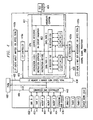
- FIG. 4 is a block diagram of a digital system 400 that has dual first level caches 410, 420 and a single second level cache 430 and that includes an embodiment of the present invention.
- Central Processing Unit (CPU) 401 which will be described in more detail below.
- a direct mapped program cache 410 having 16 kbytes capacity in cache memory 410a and L1 Program (L1P) controller 410b, is connected to the instruction fetch stage of CPU 401.
- L1P L1 Program
- a 2-way set associative data cache 420 having a 16 kbyte capacity in cache memory 420a and Level 1 Data (L1D) controller 420b is connected to data units D1 and D2 of CPU 401.
- L1D Level 1 Data
- Level 2 (L2) cache memory 430 having four banks of memory, 128 Kbytes total, is connected to L1P 410 and to L1D 420 via buses 412 and 422 respectively to provide storage for data and programs.
- Level one instruction cache (L1P) 410 stores instructions used by central processing unit core 401.
- Central processing unit core 401 first attempts to access any instruction from level one instruction cache 410.
- Level one data cache (L1D) 420 stores data used by central processing unit core 401.
- Central processing unit core 401 first attempts to access any required data from level one data cache 420.
- the two level one caches are backed by level two unified cache (L2) 430.
- the requested instruction or data is sought from level two unified cache 430. If the requested instruction or data is stored in level two unified cache 430, then it is supplied to the requesting level one cache for supply to central processing unit core 401. As is known in the art, the requested instruction or data may be simultaneously supplied to both the requesting cache and central processing unit core 401 to speed use.
- External memory interface (EMIF) 450 provides a 64 bit data path to external memory, not shown, which provides memory data to L2 cache memory 430 via extended direct memory access (DMA) controller 440.
- Extended DMA controller 440 is connected via physical address/data bus 431 to receive all read and write requests from L2 cache 430. Details of the operation of extended DMA controller are not important to the present invention; details are provided in US Patent Application S.N. 09/637,491 entitled “Data Bus Using Synchronous Latency Loop Including Read Address And Data Busses And Write Address And Data Buses", and in US Patent Application S.NO 9/637,492 entitled “Hub Interface Unit And Application Unit Interfaces For Expanded Direct Memory Access Processor".
- EMIF 452 provides a 16 bit interface for access to external peripherals, not shown.
- Expansion bus 470 provides host and I/O support.
- McBSP multi-channel buffered serial ports
- XDS external test/development system
- CPU 401 further has an instruction fetch, instruction dispatch and instruction decode pipeline, and duplicate data path 1 and data path 2.
- Data path 1 has a plurality of execution units, including an arithmetic and load/store unit D1, a multiplier M1, an ALU/shifter unit S1, an arithmetic logic unit (“ALU") L1, a shared multi-port register file A from which data are read and to which data are written.
- Decoded instructions are provided from the instruction fetch/decode pipeline to the functional units D1, M1, S1, and L1 over various sets of control lines which are not shown.
- Data are provided to/from the register file from/to load/store units D1 over a first set of busses, to multiplier M1 over a second set of busses, to ALU/shifter unit S1 over a third set of busses, and to ALU L1 over a fourth set of busses.
- Data are provided to/from the cache memory 420 from/to the load/store units D1 via a fifth set of busses. Note that the entire data path described above is duplicated in data path 2 with register file B and execution units D2, M2, S2, and L2. Instructions are fetched by the instruction fetch unit from instruction cache memory 410 over a set of busses.
- the size and configuration of the various caches are not of significance to the present invention. These are matters of design choice.
- microprocessor 400 of Figure 4 A description of various architectural features of the microprocessor 400 of Figure 4 is provided in European Patent Application No.00310098.9 filed 14th November 2000 and entitled "Microprocessor with Improved Instruction Set Architecture". A description of a basic set of instructions for microprocessor 400 is also provided in co-assigned application S.N. 09/012,813 entitled "Improved Microprocessor".
- External test system 404 is representative of a variety of known test systems for debugging and emulating integrated circuits.
- One such system is described in U.S. Patent 5,535,331 entitled Processor Condition Sensing Circuits, System, and Methods.
- Test circuitry 403 contains control registers and parallel signature analysis circuitry for testing integrated circuit 400.
- PAAM 480 is connected to physical address bus 431.
- Cacheability attribute signals 482 are connected to provide cacheability information to L2 cache 430.
- Attribute signals 484 signals are connected to provide attribute information for physical memory and devices connected to extended DMA controller 440.
- FIG. 5 is a block diagram of the digital system of Figure 4 illustrating various data transfers among the various caches, memories and devices in order to better explain the operation of PAAM 480.
- Digital signal processor system 400 includes a number of cache memories, as discussed with reference to Figure 4. The complex interrelation of parts of digital signal processor system 400 permits numerous data movements. These are illustrated schematically in Figure 5 and will now be described.
- level one program cache 410 may receive instructions recalled from level two unified cache 430 for a cache miss fill 501.
- there is no hardware support for self-modifying code so that instructions stored in level one instruction cache 410 are not altered.
- the first of these data movements is a cache miss fill 502 from level two unified cache 430 to level one data cache 420.
- Data may also pass from level one data cache 420 to level two unified cache 430, indicated at 503.
- This data movement takes place upon: a write miss to level one data cache 420 which must be serviced by level two unified cache 430; a victim eviction from level one data cache 420 to level two unified cache 430; and a snoop response from level one data cache 420 to level two unified cache 430.
- Data can be moved between level two unified cache 430 and external memory 160, indicated at 504 and 505.
- level two unified cache 430 This can take place upon: a cache miss to level two unified cache 430 service from external memory or a direct memory access 440 data movement from external memory 560 and level two unified cache 430 configured as SRAM; a victim eviction from level two unified cache 430 to external memory 560 or a direct memory access 440 data movement from a portion of level two unified cache 430 configured as SRAM to external memory 560.
- data can move between level two unified cache 430 and peripherals 570, indicated at 506 and 507.
- the number and variety of possible data movements within digital signal processor system 400 makes the problem of maintaining coherence difficult.
- data coherence is a problem.
- the cache system must control data accesses so that each returns the most recent data.
- a read following a write to the same memory address maintained within the cache must return the newly written data.
- This coherence must be maintained regardless of the processes within the cache.
- This coherence preserves the transparency of the cache system. That is, the programmer need not be concerned about the data movements within the cache and can program without regard to the presence or absence of the cache system. This transparency feature is important if the data processor is to properly execute programs written for members of a data processor family having no cache or varying amounts of cache.
- the cache hardware must maintain the programmer illusion of a single memory space.
- An example of an ordering hazard is a read from a cache entry just victimized and being evicted from the cache.
- Another example in a non-write allocate cache is a read from a cache entry following a write miss to that address with the newly written data in a write buffer waiting write to main memory.
- the cache system must include hardware to detect and handle such special cases.
- a cache system including a second level cache introduces additional hazards. Coherence must be maintained between the levels of cache no matter where the most recently written data is located. Generally level one caches accessing data will have the most recent data while the level two cache may have old data. If an access is made to the level two cache the cache system must determine if a more recent copy of the data is stored in a level one cache. This generally triggers a snoop cycle in which the level two cache polls the level one cache for more recent data before responding to the access. A snoop is nearly like a normal access to the snooped cache except that snoops are generally given higher priority.
- Snoops are granted higher priority because another level cache is stalled waiting on the response to the snoop. If the data stored in the lower level cache has been modified since the last write to the higher level cache, then this data is supplied to the higher level cache. This is referred to as a snoop hit. If the data stored in the lower level cache is clean and thus not been changed since the last write to the higher level cache, then this is noted in the snoop response but no data moves. In this case the higher level cache stores a valid copy of the data and can supply this data.
- a two level cache increases the special cases where there are hazards. Additional hazards with a two level cache include snoops to a lower level cache where the corresponding data is a victim being evicted, snoops to data in during a write miss in the lower level cache for non-write allocation systems which places the data in a write buffer. Other hazards are also possible. Details of coherence management do not affect the present invention, and are described fully in co-assigned US Patent Application S.N. 09/603,637 entitled "Multilevel Cache System Coherence With Memory Selectively Configured As Cache Or Direct Access Memory And Direct Memory Access".
- PAAM 480 operates similarly to PAAM 130, however, the proper operation of multi-level caches depends on supporting the region specifiers carefully in the caching system. For example, PC must always be honored. None of caches 410, 420 or 430 can contain a copy from an address whose region is marked with PC as 0. Similarly, all caches must honor IW. In order for the level one cache to be aware of the attribute entries, a copy of attribute bits needed by the level one cache controllers 410a/420a is provided via bus 412/422 whenever a miss occurs at the level one cache.
- Remote PAAM 551 in level two cache 430 is connected to receive and store cache attribute signals 482 in response to each entry that is stored in cache data storage memory 540.
- the PAAM 551 is associated with cache tag storage 550 so that attribute bits for each valid entry in level two cache 430 is available without needing to produce a physical address on physical address bus 431a.
- Another aspect of this embodiment of the present invention is that there are two defined PAAM bits that need to be known at the time of a cache miss. Waiting for them to be returned with the data hurts performance.
- the two bits are the WA (write allocate) bit and the SS (synchronous store) bit.
- remote PAAM 556 is implemented in level one data cache 420 and is connected to physical address bus 412a that is connected to provide addresses for requests to level two cache 430.
- CPU core 401 has two 32-bit address buses provided by data unit D1 and D2.
- a cache miss in response to either address bus results in a request on physical address bus 412b and is monitored by remote PAAM 556.
- PAAM 556 Since the reason for providing remote PAAM 556 is to deal with a cache miss, PAAM 556 is not directly associated with cache tag storage 555. Since the values are static for a given chip design, they are implemented in a small ROM as a direct mapped table. Care must be taken to assure that PAAM attribute bits in remote PAAM 556 agree with attribute bits in PAAM 480 for the same respective address ranges. In this embodiment, there is no hardware support for self-modifying code so that instructions stored in level one instruction cache 410 are not altered; therefore a remote PAAM is not needed in L1P 410.
- a remote PAAM in L1P would be advantageous, depending on configuration.
- WA and SS are only needed when a store can originate from that cache.
- Self-Modifying Code normally proceeds with a data side write that snoops the program cache and related buffers invalidating or replacing the instructions that have been written. In that arrangement, the WA and SS bits are still needed on the data cache but not on the program cache.
- PAAM 480 is connected to physical address bus 431a.
- Cacheability attribute signals 482 are connected to provide cacheability information to L2 cache 430.
- Attribute signals 484 signals are connected to transfer request circuitry 541 to provide attribute information for physical memory 560 and devices 570 that are connected to extended DMA controller 440.
- good modularity of design is provided by keeping a full copy of the PAAM info at each device.
- the processors need to cache or auto-configure information from the devices for the WA and SS bits to preserve this modularity.
- the level one instruction cache interface includes a 256-bit data path from level two unified cache 430 to level one instruction cache L1P 410.
- This data path size corresponds to one half of the 64 byte cache entry size within level one instruction cache 410 and equals one instruction fetch packet.
- the 256-bits are 64 bits from each of the four banks of level two unified cache 430.
- level two unified cache 430 can source this amount of data in a single cycle. This occurs regardless of the amount of level two unified cache 430 configured as cache.
- Level two unified cache 430 may be configured to include variable amounts of static random access memory (SRAM) instead of cache memory.
- SRAM static random access memory
- This aspect of the digital signal processor system is further detailed in co-assigned US Patent Application S.N. 09/603,645 entitled "Unified Memory System Architecture Including Cache And Addressable Static Random Access Memory”.
- the cache/SRAM partitioning within level two unified cache 430 is across the data banks rather than within the data banks.
- level two unified cache 430 can always supply 256 bits to level one instruction cache 410 if any part is partitioned as cache.
- Level one instruction cache 410 may also receive data directly from data transfer bus 543, for example upon fetching code from non-cacheable memory addresses.
- Data transfer bus 543 supplies only 64 bits per cycle, thus at least four cycles are needed to accumulate the 256 bits.
- the data source for transfers to level one instruction cache 410 is selected by multiplexer 531.
- Figure 5 illustrates supply of 32 address bits from level one instruction cache 410 to level two unified cache 430. Because level one instruction cache 410 operates on 256 bit boundaries, the 8 least significant bits are always zero and may be omitted from the address. Note that writes to level one instruction cache 410 are not permitted, therefore level one instruction cache 410 never supplies data to level two unified cache 430.
- the level one data cache interface includes a 128-bit data path from level two unified cache 430 to level one data cache 420.
- the 128 bits are 64 bits from each of two banks of level two unified cache 430. This assumes no bank conflicts with other data transfers.
- Level two unified cache 430 only services one cache fill data transfer to level one data cache 420 per cycle. Thus if two load/store units in central processing unit 401 each request data and produce a read cache miss within level one data cache 420, the two read miss requests to level two unified cache 430 are serviced in sequence.
- the cache/SRAM partitioning of level two unified cache 430 is across the memory banks.
- level two unified cache 430 can supply data to level one data cache 420 from two banks so long as level two unified cache 430 is partitioned to include some cache.
- Level one data cache 420 may also receive data directly from data transfer bus 543, for example upon fetching data from non-cacheable memory addresses.
- Data transfer bus 543 supplies only 64 bits per cycle, however accesses to non-cacheable memory addresses are at most 64 bits. In this case, the 64 bits are transferred in a single data transfer cycle.
- the data source for transfers to level one data cache 420 is selected by multiplexer 433.
- Figure 5 illustrates supply of two sets of 32 address bits via address bus 422a and address bus 423a from level one data cache 420 to level two unified cache 430. Because level one data cache 420 operates on 64 bit boundaries, the 6 least significant bits are always zero and may be omitted from the address.
- Level one data cache 420 may supply data to level two unified cache 430. This occurs on a write miss, a cache entry eviction and a response to a snoop hit to data in the modified state within level one data cache 420. It is possible that each of the load/store units within central processing unit 110 would require data transfer from level one data cache 420 to level two unified cache 430 in the same cycle.
- level one data cache 420 Upon a write miss within level one data cache 420, only the 32 bits of the write data is supplied from level one data cache 420 to L2 unified cache 430. For either a cache eviction or a snoop data response, level one data cache 420 supplies 128 bits to level two unified cache 430, the same data width as opposite transfers. Data from level one data cache 420 may also be supplied to data transfer bus 543 as selected by multiplexer 537. This could occur as a result of a write to a non-cacheable address.
- the interface between level two unified cache 430 and data transfer bus 543 includes two 64-bit data busses 431b and 431c.
- Data bus 431b supplies data from data transfer bus 543 to level two unified cache 430. This data may be stored in level two unified cache 430 via a single 64-bit write port as selected by multiplexer 535.
- Data bus 431c is a 64-bit bus supplying data from level two unified cache 430 or level one data cache 420 as selected by multiplexer 537. All transfers using data transfer bus 543 employ direct memory access unit 150 responsive to commands via transfer request bus 541.
- Physical address bus 431a comprises two physical address portions in order to allow parallel transfers on data buses 431b and 431c.
- PAAM 480 is dual ported such that both physical address portions that are present on physical address bus 431a can be monitored by PAAM 480.
- a microprocessor incorporating an aspect of the present invention to improve performance or reduce cost can be used to further improve the systems described in U.S. Patent 5,072,418.
- Such systems include, but are not limited to, industrial process controls, automotive vehicle systems, motor controls, robotic control systems, satellite telecommunication systems, echo canceling systems, modems, video imaging systems, speech recognition systems, vocoder-modem systems with encryption, and such.
- Figure 6 illustrates an exemplary implementation of an example of an integrated circuit 40 that includes digital system 400 in a mobile telecommunications device, such as a wireless telephone with integrated keyboard 12 and display 14.
- a mobile telecommunications device such as a wireless telephone with integrated keyboard 12 and display 14.
- digital system 400 with processor 401 is connected to the keyboard 12, where appropriate via a keyboard adapter (not shown), to the display 14, where appropriate via a display adapter (not shown) and to radio frequency (RF) circuitry 16.
- the RF circuitry 16 is connected to an aerial 18.
- Fabrication of digital system 400 involves multiple steps of implanting various amounts of impurities into a semiconductor substrate and diffusing the impurities to selected depths within the substrate to form transistor devices. Masks are formed to control the placement of the impurities. Multiple layers of conductive material and insulative material are deposited and etched to interconnect the various devices. These steps are performed in a clean room environment.
- a significant portion of the cost of producing the data processing device involves testing. While in wafer form, individual devices are biased to an operational state and probe tested for basic operational functionality. The wafer is then separated into individual dice which may be sold as bare die or packaged. After packaging, finished parts are biased into an operational state and tested for operational functionality.
- An integrated circuit that includes any of the above embodiments includes a plurality of contacts for surface mounting.
- the integrated circuit could include other configurations, for example a plurality of pins on a lower surface of the circuit for mounting in a zero insertion force socket, or indeed any other suitable configuration.
- Digital system 400 contains hardware extensions for advanced debugging features. These assist in the development of an application system. Since these capabilities are part of the core of CPU 401 itself, they are available utilizing only the JTAG interface with extended operating mode extensions. They provide simple, inexpensive, and speed independent access to the core for sophisticated debugging and economical system development, without requiring the costly cabling and access to processor pins required by traditional emulator systems or intruding on system resources.
- a digital system is provided with a physical address attribute map whether or not an address translation map is provided.
- signals to control certain cache memory modes are provided by the PAAM.
- capabilities specified by PAAM entries are declarative rather than imperative, that is, the attribute bits declare the capabilities of the respective device rather than giving orders to the cache as to its behavior.
- the PAAM does not require a memory management unit, or operating system control. Entries in the PAAM can be reliably set as a ROM at chip design time for many kinds of systems, including systems on a chip.
- the PAAM is associated with cacheability, write-through, sharing, readability, writeability and I/O.
- the PAAM provides control of I/O memory ordering behavior to make programming of device access simpler.
- PS when PS is used in combination with other information based on opcode or on MMU status, very fine-grained control of sharing is possible. The performance and power cost of coherence can then be carefully controlled for use on just those memory operations that are truly to shared data.
- the terms “applied,” “connected,” and “connection” mean electrically connected, including where additional elements may be in the electrical connection path.
- Associated means a controlling relationship, such as a memory resource that is controlled by an associated port.
- assert, assertion, de-assert, de-assertion, negate and negation are used to avoid confusion when dealing with a mixture of active high and active low signals. Assert and assertion are used to indicate that a signal is rendered active, or logically true. De-assert, de-assertion, negate, and negation are used to indicate that a signal is rendered inactive, or logically false.
Landscapes
- Engineering & Computer Science (AREA)
- Theoretical Computer Science (AREA)
- Software Systems (AREA)
- Physics & Mathematics (AREA)
- General Engineering & Computer Science (AREA)
- General Physics & Mathematics (AREA)
- Memory System Of A Hierarchy Structure (AREA)
Applications Claiming Priority (6)
| Application Number | Priority Date | Filing Date | Title |
|---|---|---|---|
| US18352700P | 2000-02-18 | 2000-02-18 | |
| US18341800P | 2000-02-18 | 2000-02-18 | |
| US183527P | 2000-02-18 | ||
| US183418P | 2000-02-18 | ||
| US09/702,477 US6629187B1 (en) | 2000-02-18 | 2000-10-31 | Cache memory controlled by system address properties |
| US702477 | 2000-10-31 |
Publications (1)
| Publication Number | Publication Date |
|---|---|
| EP1126375A1 true EP1126375A1 (de) | 2001-08-22 |
Family
ID=27391673
Family Applications (1)
| Application Number | Title | Priority Date | Filing Date |
|---|---|---|---|
| EP01000019A Withdrawn EP1126375A1 (de) | 2000-02-18 | 2001-02-19 | Cache-Speicher der von System-Adresseigenschaften gesteuert wird |
Country Status (2)
| Country | Link |
|---|---|
| US (1) | US6629187B1 (de) |
| EP (1) | EP1126375A1 (de) |
Families Citing this family (15)
| Publication number | Priority date | Publication date | Assignee | Title |
|---|---|---|---|---|
| US6801994B2 (en) * | 2000-12-20 | 2004-10-05 | Microsoft Corporation | Software management systems and methods for automotive computing devices |
| JP2004518343A (ja) * | 2001-01-12 | 2004-06-17 | コーニンクレッカ フィリップス エレクトロニクス エヌ ヴィ | メモリアドレス変換のための装置及び方法並びにそのような装置を含む画像処理装置 |
| US6839892B2 (en) * | 2001-07-12 | 2005-01-04 | International Business Machines Corporation | Operating system debugger extensions for hypervisor debugging |
| DE10163342A1 (de) * | 2001-12-21 | 2003-07-10 | Elektro Beckhoff Gmbh Unterneh | Datenübertragungsverfahren, serielles Bussystem und Anschalteinheit für einen passiven Busteilnehmer |
| EP1593065B1 (de) * | 2003-02-12 | 2006-06-14 | Research In Motion Limited | Verfahren, mobile vorrichtungen und rechnerlesbare media zur datenverwaltung |
| EP1471421A1 (de) * | 2003-04-24 | 2004-10-27 | STMicroelectronics Limited | Steuerung für spekulativen Ladebefehl |
| US7644135B2 (en) * | 2004-10-25 | 2010-01-05 | Texas Instruments Incorporated | Method of improving communications data throughput on embedded systems and reducing the load on the operating system and central processing unit |
| US8407432B2 (en) * | 2005-06-30 | 2013-03-26 | Intel Corporation | Cache coherency sequencing implementation and adaptive LLC access priority control for CMP |
| US20070005899A1 (en) * | 2005-06-30 | 2007-01-04 | Sistla Krishnakanth V | Processing multicore evictions in a CMP multiprocessor |
| EP2052483A2 (de) * | 2006-07-14 | 2009-04-29 | Interdigital Technology Corporation | Symbolraten-hardwarebeschleuniger |
| CN102375947A (zh) * | 2010-08-16 | 2012-03-14 | 伊姆西公司 | 用于隔离计算环境的方法和系统 |
| US8904115B2 (en) * | 2010-09-28 | 2014-12-02 | Texas Instruments Incorporated | Cache with multiple access pipelines |
| KR102117511B1 (ko) * | 2013-07-30 | 2020-06-02 | 삼성전자주식회사 | 프로세서 및 메모리 제어 방법 |
| US11556477B2 (en) * | 2018-06-15 | 2023-01-17 | Arteris, Inc. | System and method for configurable cache IP with flushable address range |
| US12561242B2 (en) | 2023-12-18 | 2026-02-24 | Samsung Electronics Co. Ltd | Method and system for locality-preserving system memory address encoding |
Citations (2)
| Publication number | Priority date | Publication date | Assignee | Title |
|---|---|---|---|---|
| EP0398189A2 (de) * | 1989-05-19 | 1990-11-22 | Compaq Computer Corporation | Direktzugriffsspeicher zur Angabe von nichtcachespeicherbaren Adressen |
| EP0598570A2 (de) * | 1992-11-13 | 1994-05-25 | Cyrix Corporation | Adressbereichkonfigurationsystem und Verfahren zur Steuerung von Speichersystemoperationen mittels Adressbereichen |
Family Cites Families (15)
| Publication number | Priority date | Publication date | Assignee | Title |
|---|---|---|---|---|
| US5329471A (en) * | 1987-06-02 | 1994-07-12 | Texas Instruments Incorporated | Emulation devices, systems and methods utilizing state machines |
| US5535331A (en) * | 1987-09-04 | 1996-07-09 | Texas Instruments Incorporated | Processor condition sensing circuits, systems and methods |
| US5072418A (en) * | 1989-05-04 | 1991-12-10 | Texas Instruments Incorporated | Series maxium/minimum function computing devices, systems and methods |
| GB9118312D0 (en) * | 1991-08-24 | 1991-10-09 | Motorola Inc | Real time cache implemented by dual purpose on-chip memory |
| JP3194201B2 (ja) * | 1992-02-24 | 2001-07-30 | 株式会社日立製作所 | キャッシュモード選択方法 |
| US5524225A (en) * | 1992-12-18 | 1996-06-04 | Advanced Micro Devices Inc. | Cache system and method for providing software controlled writeback |
| US5638537A (en) * | 1993-01-29 | 1997-06-10 | Mitsubishi Denki Kabushiki Kaisha | Cache system with access mode determination for prioritizing accesses to cache memory |
| US5623636A (en) * | 1993-11-09 | 1997-04-22 | Motorola Inc. | Data processing system and method for providing memory access protection using transparent translation registers and default attribute bits |
| US5815648A (en) * | 1995-11-14 | 1998-09-29 | Eccs, Inc. | Apparatus and method for changing the cache mode dynamically in a storage array system |
| US5813041A (en) * | 1996-06-06 | 1998-09-22 | Motorola, Inc. | Method for accessing memory by activating a programmable chip select signal |
| JPH10275080A (ja) * | 1997-01-24 | 1998-10-13 | Texas Instr Inc <Ti> | マイクロプロセッサ |
| US5940858A (en) * | 1997-05-30 | 1999-08-17 | National Semiconductor Corporation | Cache circuit with programmable sizing and method of operation |
| US6167466A (en) * | 1997-07-09 | 2000-12-26 | Texas Instruments Incorporated | Multi-channel serial port with programmable features |
| US6535958B1 (en) * | 1999-07-15 | 2003-03-18 | Texas Instruments Incorporated | Multilevel cache system coherence with memory selectively configured as cache or direct access memory and direct memory access |
| JP3641169B2 (ja) * | 1999-08-06 | 2005-04-20 | 株式会社エヌ・ティ・ティ・ドコモ | Usb対応電子機器 |
-
2000
- 2000-10-31 US US09/702,477 patent/US6629187B1/en not_active Expired - Lifetime
-
2001
- 2001-02-19 EP EP01000019A patent/EP1126375A1/de not_active Withdrawn
Patent Citations (2)
| Publication number | Priority date | Publication date | Assignee | Title |
|---|---|---|---|---|
| EP0398189A2 (de) * | 1989-05-19 | 1990-11-22 | Compaq Computer Corporation | Direktzugriffsspeicher zur Angabe von nichtcachespeicherbaren Adressen |
| EP0598570A2 (de) * | 1992-11-13 | 1994-05-25 | Cyrix Corporation | Adressbereichkonfigurationsystem und Verfahren zur Steuerung von Speichersystemoperationen mittels Adressbereichen |
Also Published As
| Publication number | Publication date |
|---|---|
| US6629187B1 (en) | 2003-09-30 |
Similar Documents
| Publication | Publication Date | Title |
|---|---|---|
| US6775750B2 (en) | System protection map | |
| US7266824B2 (en) | Address space priority arbitration | |
| US6769052B2 (en) | Cache with selective write allocation | |
| US6745293B2 (en) | Level 2 smartcache architecture supporting simultaneous multiprocessor accesses | |
| US6789172B2 (en) | Cache and DMA with a global valid bit | |
| US6779085B2 (en) | TLB operation based on task-ID | |
| US5809524A (en) | Method and apparatus for cache memory replacement line identification | |
| US6760829B2 (en) | MMU descriptor having big/little endian bit to control the transfer data between devices | |
| US6697916B2 (en) | Cache with block prefetch and DMA | |
| US6629187B1 (en) | Cache memory controlled by system address properties | |
| US6754781B2 (en) | Cache with DMA and dirty bits | |
| US6393507B2 (en) | Computer system including core logic unit with internal register for peripheral status | |
| US6968400B2 (en) | Local memory with indicator bits to support concurrent DMA and CPU access | |
| US7712098B2 (en) | Data transfer controlled by task attributes | |
| US20020069341A1 (en) | Multilevel cache architecture and data transfer | |
| EP1313014B1 (de) | Unterbrechbare und wiederaufnehmbare Instruktion zum Säubern eines Segments eines Cache-Speichers | |
| US6189049B1 (en) | Method for operating processor with internal register for peripheral status | |
| CN113849262A (zh) | 用于无需复制而在虚拟机之间移动数据的技术 | |
| US8108621B2 (en) | Data cache with modified bit array | |
| US6374320B1 (en) | Method for operating core logic unit with internal register for peripheral status | |
| JP4490585B2 (ja) | 周辺ステータスについての内部レジスタを有するプロセッサまたはコア論理演算装置 | |
| US8108624B2 (en) | Data cache with modified bit array | |
| US20010008003A1 (en) | Processor with internal register for peripheral status | |
| JP2001273192A (ja) | マイクロプロセッサを有するディジタル・システム及びそのディジタル・システムを動作させる方法 | |
| JPH0981458A (ja) | データ処理システムにおけるキャッシュのアクセス方法 |
Legal Events
| Date | Code | Title | Description |
|---|---|---|---|
| PUAI | Public reference made under article 153(3) epc to a published international application that has entered the european phase |
Free format text: ORIGINAL CODE: 0009012 |
|
| AK | Designated contracting states |
Kind code of ref document: A1 Designated state(s): AT BE CH CY DE DK ES FI FR GB GR IE IT LI LU MC NL PT SE TR |
|
| AX | Request for extension of the european patent |
Free format text: AL;LT;LV;MK;RO;SI |
|
| 17P | Request for examination filed |
Effective date: 20020222 |
|
| AKX | Designation fees paid |
Free format text: AT BE CH CY DE DK ES FI FR GB GR IE IT LI LU MC NL PT SE TR |
|
| 17Q | First examination report despatched |
Effective date: 20020722 |
|
| 17Q | First examination report despatched |
Effective date: 20020722 |
|
| STAA | Information on the status of an ep patent application or granted ep patent |
Free format text: STATUS: THE APPLICATION IS DEEMED TO BE WITHDRAWN |
|
| 18D | Application deemed to be withdrawn |
Effective date: 20070913 |