EP0398244A2 - Mémoire à accès aléatoire de type dynamique - Google Patents
Mémoire à accès aléatoire de type dynamique Download PDFInfo
- Publication number
- EP0398244A2 EP0398244A2 EP90109122A EP90109122A EP0398244A2 EP 0398244 A2 EP0398244 A2 EP 0398244A2 EP 90109122 A EP90109122 A EP 90109122A EP 90109122 A EP90109122 A EP 90109122A EP 0398244 A2 EP0398244 A2 EP 0398244A2
- Authority
- EP
- European Patent Office
- Prior art keywords
- bit line
- potential
- charge transfer
- sense
- sense amplifier
- Prior art date
- Legal status (The legal status is an assumption and is not a legal conclusion. Google has not performed a legal analysis and makes no representation as to the accuracy of the status listed.)
- Withdrawn
Links
- 238000012546 transfer Methods 0.000 claims abstract description 97
- 238000003199 nucleic acid amplification method Methods 0.000 claims abstract description 16
- 230000003321 amplification Effects 0.000 claims abstract description 15
- 230000003247 decreasing effect Effects 0.000 claims description 32
- 230000005669 field effect Effects 0.000 claims description 4
- 230000003334 potential effect Effects 0.000 claims description 3
- 239000000543 intermediate Substances 0.000 description 15
- 239000012535 impurity Substances 0.000 description 7
- 238000005468 ion implantation Methods 0.000 description 7
- 239000003990 capacitor Substances 0.000 description 6
- 239000000758 substrate Substances 0.000 description 6
- XUIMIQQOPSSXEZ-UHFFFAOYSA-N Silicon Chemical compound [Si] XUIMIQQOPSSXEZ-UHFFFAOYSA-N 0.000 description 4
- 230000004913 activation Effects 0.000 description 4
- 238000010586 diagram Methods 0.000 description 4
- 150000002500 ions Chemical class 0.000 description 4
- 238000012986 modification Methods 0.000 description 4
- 230000004048 modification Effects 0.000 description 4
- 229910052710 silicon Inorganic materials 0.000 description 4
- 239000010703 silicon Substances 0.000 description 4
- 230000000694 effects Effects 0.000 description 3
- 238000004519 manufacturing process Methods 0.000 description 2
- 239000004065 semiconductor Substances 0.000 description 2
- 230000015572 biosynthetic process Effects 0.000 description 1
- 230000001747 exhibiting effect Effects 0.000 description 1
- 238000002513 implantation Methods 0.000 description 1
- 229910021420 polycrystalline silicon Inorganic materials 0.000 description 1
Images





Classifications
-
- G—PHYSICS
- G11—INFORMATION STORAGE
- G11C—STATIC STORES
- G11C11/00—Digital stores characterised by the use of particular electric or magnetic storage elements; Storage elements therefor
- G11C11/21—Digital stores characterised by the use of particular electric or magnetic storage elements; Storage elements therefor using electric elements
- G11C11/34—Digital stores characterised by the use of particular electric or magnetic storage elements; Storage elements therefor using electric elements using semiconductor devices
- G11C11/40—Digital stores characterised by the use of particular electric or magnetic storage elements; Storage elements therefor using electric elements using semiconductor devices using transistors
- G11C11/401—Digital stores characterised by the use of particular electric or magnetic storage elements; Storage elements therefor using electric elements using semiconductor devices using transistors forming cells needing refreshing or charge regeneration, i.e. dynamic cells
- G11C11/4063—Auxiliary circuits, e.g. for addressing, decoding, driving, writing, sensing or timing
- G11C11/407—Auxiliary circuits, e.g. for addressing, decoding, driving, writing, sensing or timing for memory cells of the field-effect type
-
- G—PHYSICS
- G11—INFORMATION STORAGE
- G11C—STATIC STORES
- G11C11/00—Digital stores characterised by the use of particular electric or magnetic storage elements; Storage elements therefor
- G11C11/21—Digital stores characterised by the use of particular electric or magnetic storage elements; Storage elements therefor using electric elements
- G11C11/34—Digital stores characterised by the use of particular electric or magnetic storage elements; Storage elements therefor using electric elements using semiconductor devices
- G11C11/40—Digital stores characterised by the use of particular electric or magnetic storage elements; Storage elements therefor using electric elements using semiconductor devices using transistors
- G11C11/401—Digital stores characterised by the use of particular electric or magnetic storage elements; Storage elements therefor using electric elements using semiconductor devices using transistors forming cells needing refreshing or charge regeneration, i.e. dynamic cells
- G11C11/4063—Auxiliary circuits, e.g. for addressing, decoding, driving, writing, sensing or timing
- G11C11/407—Auxiliary circuits, e.g. for addressing, decoding, driving, writing, sensing or timing for memory cells of the field-effect type
- G11C11/409—Read-write [R-W] circuits
- G11C11/4096—Input/output [I/O] data management or control circuits, e.g. reading or writing circuits, I/O drivers or bit-line switches
-
- G—PHYSICS
- G11—INFORMATION STORAGE
- G11C—STATIC STORES
- G11C11/00—Digital stores characterised by the use of particular electric or magnetic storage elements; Storage elements therefor
- G11C11/21—Digital stores characterised by the use of particular electric or magnetic storage elements; Storage elements therefor using electric elements
- G11C11/34—Digital stores characterised by the use of particular electric or magnetic storage elements; Storage elements therefor using electric elements using semiconductor devices
- G11C11/40—Digital stores characterised by the use of particular electric or magnetic storage elements; Storage elements therefor using electric elements using semiconductor devices using transistors
- G11C11/401—Digital stores characterised by the use of particular electric or magnetic storage elements; Storage elements therefor using electric elements using semiconductor devices using transistors forming cells needing refreshing or charge regeneration, i.e. dynamic cells
- G11C11/4063—Auxiliary circuits, e.g. for addressing, decoding, driving, writing, sensing or timing
- G11C11/407—Auxiliary circuits, e.g. for addressing, decoding, driving, writing, sensing or timing for memory cells of the field-effect type
- G11C11/409—Read-write [R-W] circuits
-
- G—PHYSICS
- G11—INFORMATION STORAGE
- G11C—STATIC STORES
- G11C11/00—Digital stores characterised by the use of particular electric or magnetic storage elements; Storage elements therefor
- G11C11/21—Digital stores characterised by the use of particular electric or magnetic storage elements; Storage elements therefor using electric elements
- G11C11/34—Digital stores characterised by the use of particular electric or magnetic storage elements; Storage elements therefor using electric elements using semiconductor devices
- G11C11/40—Digital stores characterised by the use of particular electric or magnetic storage elements; Storage elements therefor using electric elements using semiconductor devices using transistors
- G11C11/401—Digital stores characterised by the use of particular electric or magnetic storage elements; Storage elements therefor using electric elements using semiconductor devices using transistors forming cells needing refreshing or charge regeneration, i.e. dynamic cells
- G11C11/4063—Auxiliary circuits, e.g. for addressing, decoding, driving, writing, sensing or timing
- G11C11/407—Auxiliary circuits, e.g. for addressing, decoding, driving, writing, sensing or timing for memory cells of the field-effect type
- G11C11/409—Read-write [R-W] circuits
- G11C11/4091—Sense or sense/refresh amplifiers, or associated sense circuitry, e.g. for coupled bit-line precharging, equalising or isolating
Definitions
- the present invention relates to a semiconductor memory and, more particularly, to a semiconductor memory having a bit line potential read circuit portion in a dynamic type random-access memory (to be abbreviated to as a DRAM hereinafter).
- a DRAM dynamic type random-access memory
- charge transfer transistors NT1 and NT2 comprising insulating gate type MOS field effect transistors are connected between first and second bit lines BL and BL constituting the bit line pair of each column, and a bit line sense amplifier NA, as shown in Fig. 1.
- reference symbols BL and BL denote first and second bit lines constituting the bit line pair of each column in a memory cell array of a DRAM.
- the transistors TW0 and TW1 are enabled by a precharge signal EQ L (bit line precharge dummy
- Reference symbol PR denotes a precharge equalize circuit for precharging and equalizing the first and second bit lines BL and BL constituting the bit line pair of each column to a precharge voltage V BL (which is set to be, e.g., 1/2 a power source voltage V CC ).
- the precharge equalize circuit PR is enabled by the precharge signal EQL .
- Reference symbol PA denotes a bit line restore p-channel sense amplifier comprising p-channel MOS transistors P1 and P2. The drain of the transistor P1 is connected to the bit line BL, and the drain of the transistor P2 is connected to the bit line BL .
- the gate of the transistor P1 is connected to the drain of the transistor P2, and the gate of the transistor P2 is connected to the drain of the transistor P1.
- the sense amplifier PA is enabled by a p-channel sense amplifier enable signal SAP j .
- Reference symbol NA denotes an n-channel sense amplifier comprising n-channel MOS transistors N1 and N2.
- the drain of the transistor N1 is connected to a sense node SN, and the drain of the transistor N2 is connected to a sense node SN .
- the gate of the transistor N1 is connected to the sense node SN , and the gate of the transistor N2 is connected to the sense node SN.
- the drain of the transistor N1 is connected to one current path of the charge transfer transistor NT1, and the drain of the transistor N2 is connected to one current path of the charge transfer transistor NT2.
- the sense amplifier NA is enabled by an n-channel sense amplifier enable signal SAN j .
- the charge transfer transistors NT1 and NT2 receive a drive signal ⁇ Tj from a charge transfer transistor driver (not shown), and are controlled to be kept OFF for a predetermined period of time from a timing immediately before the n-channel sense amplifier NA is enabled.
- the pair of sense nodes SN and SN of the bit line sense amplifier NA are connected to a pair of column selection transistors CT1 and CT2.
- the pair of column selection transistors CT1 and CT2 are respectively connected to a pair of data buses DL1 and DL2 through a pair of data lines DQ1 and DQ2 commonly connected to a plurality of columns and through a data buffer DQB.
- V CC potential is, e.g., 5 V
- both the first and second bit lines BL and BL are kept at V CC /2.
- RAS row address strobe signal
- a row address is written, and is determined in the memory chip.
- the row address is decoded, and the word line WL1 on the side of the first bit line BL is selected to turn on the charge transfer transistor TM of the selected memory cell MC1.
- the potential of data 0 V (“L" level) is read out from a capacitor C1 of this memory cell MC1, and the potential of the first bit line BL is slightly decreased from V CC /2.
- the dummy word line DWL0 on the side of the second bit line BL is simultaneously selected, thus turning on the charge transfer transistor TD of the dummy cell DC0. Since a potential of V DC (e.g., V CC /2) is written in advance in the dummy cell DC0, even if the charge transfer transistor TD is turned on and a capacitor C0 of the dummy cell DC0 is short-circuited to the second bit line BL , the potential of the second bit line BL is left unchanged at V CC /2 since the capacitor C0 and the second bit line BL have the same potential.
- V DC e.g., V CC /2
- the charge transfer transistor drive signal ⁇ Tj goes to a V SS potential for a predetermined period of time ⁇ 2, and the charge transfer transistors NT1 and NT2 are turned off for a predetermined period of time.
- the first and second bit lines BL and BL as the bit line pair are disconnected from the n-channel sense amplifier NA, i.e., are set in a floating state for a predetermined period of time.
- the n-channel sense amplifier enable signal SAN j goes to the V SS potential, thereby enabling the n-channel sense amplifier NA.
- a small potential difference between the pair of first and second sense nodes SN and SN of the n-channel sense amplifier NA is sense-amplified by the n-channel sense amplifier NA.
- the n-channel sense amplifier NA When the n-channel sense amplifier NA is enabled, the potential of the sense node SN of the n-channel sense amplifier NA is decreased to 0 V.
- the signal ⁇ Tj is returned to the V CC potential and the charge transfer transistors NT1 and NT2 are returned from an OFF to ON state, the first and second bit lines BL and BL are respectively connected to the corresponding first and second sense nodes SN and SN of the n-channel sense amplifier NA, and the potential of the first bit line BL is decreased toward 0 V.
- the signal SAP j goes to the V CC potential to enable the p-channel sense amplifier PA, and the potential of the second bit line BL is increased toward V CC potential by the p-channel sense amplifier PA.
- a column address strobe signal CAS is enabled, and a column address is decoded.
- the pair of column selection transistors CT1 and CT2 are turned on, the potentials of the pair of sense nodes SN and SN of the sense amplifier NA are reamplified by the data buffer DQB through the pair of data lines DQ1 and DQ2, and the amplified potentials are output to the pair of data buses DL1 and DL2.
- the word line WL1 and the dummy word line DWL0 are returned to a non-selected state.
- the precharge signal EQL goes to the VCC potential, so that the bit lines BL and BL are precharged to a voltage of V BL , and the dummy cells DC0 and DC1 are precharged to a voltage of V DC .
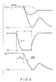
- Fig. 3 shows in enlarged scales changes in potentials of the sense nodes SN and SN , and changes in potentials of the first and second bit lines BL and BL .
- the capacitances of the sense nodes SN and SN of the n-channel sense amplifier NA become very small since the charge transfer transistors NT1 and NT2 are turned off and the bit lines BL and BL are disconnected from the n-channel sense amplifier NA after the charge transfer transistor drive signal ⁇ Tj goes to the V SS potential.
- the capacitances of the sense nodes SN and SN become very sensitive to the asymmetry of the sense nodes SN and SN of the n-channel sense amplifier NA.
- the n-channel sense amplifier enable signal SAN j goes to the V SS potential
- the relationship between the potentials of the sense nodes SN and SN may often be reversed under the influence of the asymmetry of the sense nodes SN and SN .
- the n-channel sense amplifier NA performs amplification in this reversed state, the potential of the sense node SN is erroneously decreased toward 0 V, resulting in an erroneous operation of the n-channel sense amplifier NA.
- the asymmetry of the sense nodes SN and SN of the n-channel sense amplifier NA is mainly caused by oblique ion-implantation, as shown in Fig. 4, employed to form a low-concentration impurity region upon formation of an LDD (lightly doped drain) transistor if an n-channel transistor of an LDD structure is used as the n-channel transistor used in the n-channel sense amplifier NA.
- reference numeral 90 denotes a p-type silicon substrate; 91 and 92, a high-concentration impurity (n+-type) region and a low-concentration impurity (n ⁇ -type) region; and 93, a gate electrode formed of, e.g., polycrystalline silicon.
- ion-implantation for forming the n ⁇ -type region 92 is normally performed to be inclined at 7° with respect to the surface of the silicon substrate 90.
- a portion where no ions are implanted is formed behind the gate electrode 93 and the LDD transistor has an asymmetrical shape, thus exhibiting asymmetrical electrical characteristics.
- the asymmetry of the electrical characteristics can be reduced by performing ion-implantation while rotating the substrate 90 through 90° with respect to the first ion-implantation direction or forming a thin oxide film on the substrate 90 so as not to allow deep implantation of the impurity ions and then performing ion-implantation from a direction at an ion-implantation angle of 0°.
- asymmetry to some extent inevitably occurs due to variations in manufacturing process. Therefore, a source-drain current varies depending on the selection of the two regions as the source and drain regions.
- a region shaded with the gate electrode has a small capacitance to the gate, and the other region has a large capacitance to the gate.
- Such asymmetry causes asymmetrical electrical characteristics of the LDD transistor described above.
- a DRAM in which the charge transfer transistors are controlled to be turned off for a predetermined period of time from a timing immediately before the sense amplifier is enabled can perform high-speed sense amplification.
- the DRAM is easily influenced by the asymmetry of the sense nodes of the sense amplifier, and the sense amplifier may easily cause an erroneous operation.
- a DRAM comprises: a bit line pair consisting of first and second bit lines; a memory cell array including a plurality of memory cells connected to the bit line pair; a precharge circuit for precharging the bit line pair to a predetermined voltage at a predetermined timing; a bit line sense amplifier which is enabled after data written in one of the plurality of memory cells is read out onto the bit line pair; and a charge transfer circuit which is connected between the bit lines and sense nodes of the bit line sense amplifier, and is kept OFF for a predetermined period of time after a sense amplification operation of the bit line sense amplifier is started.
- both the first and second bit lines are equally kept at a bit line precharge voltage during a period from an enable timing of an RAS signal until a word line goes to selection level.
- a word line is selected, data 0 V is read out from the selected memory cell, and the potential of the first bit line is slightly decreased from the bit line precharge voltage.
- the bit line sense amplifier is enabled, and sense-amplifies the small potential difference between the first and second bit lines.
- the potential of the first sense node is decreased toward 0 V.
- the charge transfer circuit is turned off for a predetermined period of time, and the bit line pair are disconnected from the bit line sense amplifier for the predetermined period of time.
- the word line is returned to a non-selected state. Furthermore, a precharge signal is enabled, and the bit line pair are respectively precharged.
- the charge transfer circuit is controlled to be kept OFF for a predetermined period of time after the bit line sense amplifier is enabled, a high-speed sense amplification operation is allowed immediately after the loads of the sense nodes are reduced. Even when asymmetry of the sense nodes of the bit line sense amplifier occurs unavoidably, the bit line sense amplifier has already been enabled when the loads of the sense nodes are reduced. Therefore, the capacitances of the sense nodes will not become too small, and the DRAM can be prevented from being easily influenced by the asymmetry and from causing an erroneous operation of the sense amplifier.
- Fig. 1 shows a portion of a DRAM according to the present invention.
- the DRAM of the present invention has a different OFF controlling timing of charge transfer transistors NT1 and NT2 as compared to a conventional DRAM which employs a charge transfer transistor driving system (a system in which the charge transfer transistors NT1 and NT2 are controlled to be kept OFF from a timing immediately before an n-channel sense amplifier is enabled) described above with reference to Fig. 2. More specifically, as compared to the conventional DRAM, according to this embodiment, an n-channel sense amplifier enable signal SAN j is decreased to a V SS potential before a charge transfer transistor drive signal ⁇ Tj is decreased to the V SS potential.
- This embodiment has the same circuit arrangement as that of the prior art shown in Fig. 1, and this embodiment will be described below with reference to Fig. 1.
- an n-channel sense amplifier NA is enabled after a signal is read out from a memory cell onto a bit line, and the charge transfer transistors NT1 and NT2 are controlled to be OFF after the sense amplification operation of the n-channel sense amplifier NA.
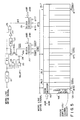
- FIG. 5 schematically shows a portion of a drive signal supply system in, e.g., a 4-Mbit DRAM employing the above-mentioned charge transfer transistor driving system.
- a memory cell array MA is divided into eight blocks BL0 to BL7 in correspondence with combinations of upper three addresses A 8R , A 9R , and A 10R .
- a sense amplifier/column decoder SA ⁇ CD is arranged at a central portion in the column direction of each block (including 512K cells), and a row decoder RD is arranged at one end portion in a row direction of each block. In one cycle, two blocks can be simultaneously enabled.
- Reference numerals 21 to 23 denote delay circuits; 24 and 25, NOR gates; 26, a NAND gate; 27 and 28, inverters; and 29 and 30, block decoders.
- V CC potential is, e.g., 5 V
- both first and second bit lines BL and BL are kept at V CC /2.
- Row and column addresses are sequentially input as address inputs, and a row address strobe signal RAS is enabled after the row address is input. Thereafter, a precharge signal EQL is disabled. When the signal RAS is enabled, the row address is fetched, and is determined in the memory chip.
- the row address is decoded, and a word line WL1 on the side of the first bit line BL is selected to turn on a charge transfer transistor TM of the selected memory cell MC1.
- a word line WL1 on the side of the first bit line BL is selected to turn on a charge transfer transistor TM of the selected memory cell MC1.
- the potential of data 0 V (“L" level) is read out from a capacitor C1 of this memory cell MC1, and the potential of the first bit line BL is slightly decreased from V CC /2.
- a dummy word line DWL0 on the side of the second bit line BL is selected to turn on a charge transfer transistor TD of a dummy cell DC0.
- a potential of V DC e.g., V CC /2
- V DC e.g., V CC /2
- a control signal SAN is decreased to V SS .
- the block decoder 29 decodes the two addresses A 8R and A 9R , and two of sense amplifier enable signals SAN0 to SAN7 (one of these signals corresponds to an n-channel sense amplifier enable signal SAN j ) selectively go to the V SS potential.
- the n-channel sense amplifier NA in the selected block are thus enabled to perform a sense amplification operation. As a result, the potential of its first sense node SN is decreased toward 0 V.
- a control signal ⁇ Tj is decreased to the V SS potential for a predetermined period of time ⁇ 6.
- the block decoder 30 decodes the two addresses A 8R and A 9R , and two of charge transfer transistor drive signals ⁇ T0 to ⁇ T7 (one of these signals corresponds to a charge transfer transistor drive signal ⁇ Tj ) selectively go to the V SS potential only for the predetermined period of time ⁇ 6.
- the charge transfer transistors NT1 and NT2 in the selected block are turned off only for the predetermined period of time ⁇ 6.
- the bit lines BL and BL are disconnected from the n-channel sense amplifier NA for the predetermined period of time ⁇ 6.
- bit lines BL and BL are connected to the pair of sense nodes SN and SN of the bit line sense amplifier NA, and the potential of the first bit line BL is decreased to 0 V. Furthermore, a p-channel sense amplifier enable signal SAP j is changed from a V CC /2 potential to the V CC potential to enable a p-channel sense amplifier PA, and the potential of the second bit line BL is increased toward the V CC potential by the p-channel sense amplifier PA.
- a column address strobe signal CAS is enabled, and a column address is decoded to turn on column selection transistors CT1 and CT2.
- the potentials of the pair of sense nodes SN and SN of the sense amplifier NA are reamplified by a data buffer DQB via a pair of data lines DQ1 and DQ2, and the amplified potentials are output onto a pair of data buses DL1 and DL2.
- a precharge signal EQL is enabled, so that the bit lines BL and BL are precharged to a voltage of V BL , and the dummy cells DC0 and DC1 are precharged to a voltage of V DC .
- the n-channel sense amplifier NA is enabled to perform a sense amplification operation. Thereafter, the charge transfer transistors NT1 and NT2 are turned off for a predetermined period of time, and the capacitances of the bit lines BL and BL are completely disconnected from the n-channel sense amplifier NA for the predetermined period of time. When the capacitances of the bit lines BL and BL are disconnected from the n-channel sense amplifier NA, the loads of the sense nodes SN and SN are immediately reduced. From this timing, a sensing speed of the sense node SN is remarkably increased, and high-speed sense amplification is allowed.
- the charge transfer transistors NT1 and NT2 are kept OFF only for a delay time ⁇ 6, and the bit lines BL and BL are disconnected from the n-channel sense amplifier NA for the predetermined period of time.
- the bit lines BL and BL are disconnected from the sense amplifier NA, the loads of the sense nodes SN and are reduced, and high-speed sense amplification can be normally performed.
- the delay time ⁇ 5 required from when the signal SAN j begins to fall toward the ground potential V SS and the potential difference ⁇ V BL almost equal to that at the beginning of activation is recovered to the sense nodes SN and SN is as short as 3 to 4 ns in the worst case since the capacitances of the sense nodes SN and SN are as very small as 100 fF or less and is negligible.
- the charge transfer transistor drive signal ⁇ Tj is decreased from V CC potential to the V SS potential.
- the signal may be decreased to an intermediate potential V M between the V CC and V SS potentials.
- a DRAM which employs a charge transfer transistor driving system in which the charge transfer transistor drive signal ⁇ Tj is decreased to the intermediate potential V M when the charge transfer transistors NT1 and NT2 are turned off, will be described in detail below.
- the read and rewrite operations with respect to this DRAM are performed according to the operations of the embodiment described above, except for the following operations. That is, when a signal is read out from a memory cell and a dummy cell, and the small potential difference ⁇ V BL occurs between the potentials of the first and second bit lines BL and BL , the n-channel sense amplifier NA is enabled to perform initial amplification. Thereafter, the signal ⁇ Tj is decreased from the V CC potential to the intermediate potential V M to turn off the charge transfer transistors NT1 and NT2. As a result, the bit lines BL and BL are disconnected from the n-channel sense amplifier NA.
- the potentials of the first sense node SN and the first bit line BL are decreased to 0 V while approaching each other.
- the potential of the first bit line BL is rewritten in the selected memory cell MC1
- the potential of the second bit line BL is rewritten in the dummy cell DC0.
- the signal ⁇ Tj is returned to the V CC potential, and the charge transfer transistors NT1 and NT2 are returned to an ON state.
- the charge transfer transistors NT1 and NT2 are returned to the ON state, a charge is suddenly redistributed to the first sense node SN and the first bit line BL.
- the potential of the first sense node SN having a smaller capacitance rises slightly earlier than that of the first bit line BL, the potentials of the first sense node SN and the first bit line BL are considerably close to each other, and the potential of the first sense node SN will not immediately rise.
- the intermediate potential V M is set to satisfy V TN ⁇ V M ⁇ V BL + V TN .
- the charge transfer transistors NT1 and NT2 are turned off at the beginning of the sense operation of the sense amplifier NA and are turned on before the sense amplifier NA completes a sense operation, the same effect as in the above embodiment can be obtained.
- V M may be set to satisfy V TN + ⁇ ⁇ V M ⁇ V BL + V TN - ⁇ .
- Fig. 8 shows a modification of the DRAM shown in Fig. 1. Differences between the DRAMs shown in Figs. 8 and 1 are that the n- and p-channel sense amplifiers NA and PA are replaced with each other, p-channel charge transfer transistors PT1 and PT2 are used in place of the n-channel charge transfer transistors NT1 and NT2, and the logic level of the charge transfer transistor drive signal ⁇ Tj is inverted.
- Other arrangements are the same as those in Fig. 1, and the same reference numerals in Fig. 8 denote the same parts as in the above embodiment.
- the charge transfer transistor drive signal ⁇ Tj is increased from the V SS potential to the V CC potential or the intermediate potential V M when the charge transfer transistors PT1 and PT2 are turned off; otherwise, the signal is decreased to the V SS potential.
- the intermediate potential V M of the charge transfer transistor drive signal ⁇ Tj is set to satisfy V BL -
- the operation of the DRAM employing the charge transfer transistor driving system in which the charge transfer transistor drive signal ⁇ Tj is increased from the V SS potential to the intermediate potential V M when the charge transfer transistors PT1 and PT2 are turned off is performed according to the operation of the DRAM employing the charge transfer transistor driving system in which the charge transfer transistor drive signal ⁇ Tj is decreased from the V CC potential to the intermediate potential V M , and the same effect as described above can be obtained.
- the relationship among the bit line precharge voltage V BL , the threshold voltage V TP of the p-channel charge transfer transistors PT1 and PT2, and the intermediate potential V M is determined to satisfy V BL -
- the charge transfer transistors PT1 and PT2 are turned off at the beginning of the sense operation of the sense amplifier PA and are turned on before the sense amplifier PA completes a sense operation, the same effect as in the above embodiment can be obtained.
- the relationship among the bit line precharge voltage V BL , the threshold voltage V TP of the p-channel charge transfer transistors PT1 and PT2, and the intermediate potential VM may be set to satisfy V BL -
- the charge transfer transistors NT1 and NT2 or PT1 and PT2 need not always be connected between the pair of bit lines BL and BL and the pair of sense nodes SN and SN .
- a charge transfer circuit having characteristics equivalent to the above-mentioned charge transfer transistors may be connected.
- the charge transfer circuit can be controlled to be temporarily turned off when a small potential difference occurs between the bit lines BL and BL in a read mode of memory cell data.
- the impedance is changed according to a potential difference between two terminals of bit lines and sense nodes as in the above-mentioned charge transfer transistors, and an element is connected between a bit line side terminal and a bit line sense amplifier side terminal. This element is turned off by a potential difference between a third terminal and one of the two terminals.
- the impedance of the charge transfer circuit is gradually decreased, so that the sense nodes and the bit lines can be naturally and slowly connected to each other.
- a high-speed sense operation can be assured, and a temporary decrease in potential difference between the sense nodes SN and SN when the charge transfer circuit is returned to an ON state can be suppressed.
- Figs. 9A and 9B show other charge transfer circuits.
- a diode D comprising a bipolar NPN transistor whose collector and base are connected to each other is connected between two terminals, and a switching circuit S is connected in parallel with the diode D, and the switching circuit S is switching-controlled.
- the switching circuit S is turned off at the beginning of activation of the bit line sense amplifier, the pair of sense nodes SN and SN are disconnected from the bit lines BL and BL .
- the impedance of the diode D is gradually decreased, and the potential differences between the bit lines BL and BL and between the sense nodes SN and SN are amplified.
- the switching circuit S is turned on again, the potential difference between the bit lines BL and BL can be sufficiently increased.
Landscapes
- Engineering & Computer Science (AREA)
- Microelectronics & Electronic Packaging (AREA)
- Computer Hardware Design (AREA)
- Databases & Information Systems (AREA)
- Dram (AREA)
Applications Claiming Priority (2)
| Application Number | Priority Date | Filing Date | Title |
|---|---|---|---|
| JP1121209A JPH02301097A (ja) | 1989-05-15 | 1989-05-15 | ダイナミック型ランダムアクセスメモリ |
| JP121209/89 | 1989-05-15 |
Publications (2)
| Publication Number | Publication Date |
|---|---|
| EP0398244A2 true EP0398244A2 (fr) | 1990-11-22 |
| EP0398244A3 EP0398244A3 (fr) | 1992-06-17 |
Family
ID=14805577
Family Applications (1)
| Application Number | Title | Priority Date | Filing Date |
|---|---|---|---|
| EP19900109122 Withdrawn EP0398244A3 (fr) | 1989-05-15 | 1990-05-15 | Mémoire à accès aléatoire de type dynamique |
Country Status (3)
| Country | Link |
|---|---|
| EP (1) | EP0398244A3 (fr) |
| JP (1) | JPH02301097A (fr) |
| KR (1) | KR900019040A (fr) |
Cited By (9)
| Publication number | Priority date | Publication date | Assignee | Title |
|---|---|---|---|---|
| EP0499256A1 (fr) * | 1991-02-13 | 1992-08-19 | Kabushiki Kaisha Toshiba | Dispositif de mémoire à semi-conducteur |
| GB2259384A (en) * | 1991-08-14 | 1993-03-10 | Samsung Electronics Co Ltd | Data transmission circuits for memory devices |
| US5317540A (en) * | 1991-03-14 | 1994-05-31 | Kabushiki Kaisha Toshiba | Semiconductor memory device |
| US5341326A (en) * | 1991-02-13 | 1994-08-23 | Kabushiki Kaisha Toshiba | Semiconductor memory having memory cell units each including cascade-connected MOS transistors |
| US5359566A (en) * | 1991-05-29 | 1994-10-25 | Kabushiki Kaisha Toshiba | Dynamic random access memory |
| US5369612A (en) * | 1990-06-27 | 1994-11-29 | Kabushiki Kaisha Toshiba | Semiconductor memory device |
| EP0663666A3 (fr) * | 1994-01-12 | 1995-10-04 | Siemens Ag | Circuit intégré de mémoire à semi-conducteurs et méthode d'opération. |
| US5500815A (en) * | 1991-11-27 | 1996-03-19 | Kabushiki Kaisha Toshiba | Semiconductor memory |
| US5525820A (en) * | 1990-04-20 | 1996-06-11 | Kabushiki Kaisha Toshiba | Semiconductor memory cell |
Families Citing this family (4)
| Publication number | Priority date | Publication date | Assignee | Title |
|---|---|---|---|---|
| JP2523879B2 (ja) * | 1989-06-16 | 1996-08-14 | 松下電器産業株式会社 | センスアンプ回路 |
| US5684750A (en) * | 1996-03-29 | 1997-11-04 | Mitsubishi Denki Kabushiki Kaisha | Semiconductor memory device with a sense amplifier including two types of amplifiers |
| JP2008077805A (ja) | 2006-09-25 | 2008-04-03 | Fujitsu Ltd | 半導体記憶装置及びタイミング制御方法 |
| KR101036926B1 (ko) | 2009-12-30 | 2011-05-25 | 주식회사 하이닉스반도체 | 반도체 메모리 장치 |
Family Cites Families (4)
| Publication number | Priority date | Publication date | Assignee | Title |
|---|---|---|---|---|
| JPS5925311B2 (ja) * | 1977-02-14 | 1984-06-16 | 日本電気株式会社 | 感知増幅器 |
| DE2712735B1 (de) * | 1977-03-23 | 1978-09-14 | Ibm Deutschland | Lese-/Schreibzugriffschaltung zu Speicherzellen eines Speichers und Verfahren zu ihrem Betrieb |
| JPS5472641A (en) * | 1977-11-21 | 1979-06-11 | Toshiba Corp | Voltage detection circuit |
| JP2763772B2 (ja) * | 1987-07-15 | 1998-06-11 | オリンパス光学工業株式会社 | コネクタ装置 |
-
1989
- 1989-05-15 JP JP1121209A patent/JPH02301097A/ja active Pending
-
1990
- 1990-05-15 EP EP19900109122 patent/EP0398244A3/fr not_active Withdrawn
- 1990-05-15 KR KR1019900007092A patent/KR900019040A/ko not_active Abandoned
Cited By (14)
| Publication number | Priority date | Publication date | Assignee | Title |
|---|---|---|---|---|
| US5525820A (en) * | 1990-04-20 | 1996-06-11 | Kabushiki Kaisha Toshiba | Semiconductor memory cell |
| US5369612A (en) * | 1990-06-27 | 1994-11-29 | Kabushiki Kaisha Toshiba | Semiconductor memory device |
| US5410505A (en) * | 1990-06-27 | 1995-04-25 | Kabushiki Kaisha Toshiba | Semiconductor memory device having a memory cell unit including a plurality of transistors connected in series |
| US5341326A (en) * | 1991-02-13 | 1994-08-23 | Kabushiki Kaisha Toshiba | Semiconductor memory having memory cell units each including cascade-connected MOS transistors |
| EP0499256A1 (fr) * | 1991-02-13 | 1992-08-19 | Kabushiki Kaisha Toshiba | Dispositif de mémoire à semi-conducteur |
| US5432733A (en) * | 1991-02-13 | 1995-07-11 | Kabushiki Kaisha Toshiba | Semiconductor memory device |
| US5444652A (en) * | 1991-02-13 | 1995-08-22 | Kabushiki Kaisha Toshiba | Semiconductor memory device having a memory cell unit including a plurality of transistors connected in series |
| US5317540A (en) * | 1991-03-14 | 1994-05-31 | Kabushiki Kaisha Toshiba | Semiconductor memory device |
| US5359566A (en) * | 1991-05-29 | 1994-10-25 | Kabushiki Kaisha Toshiba | Dynamic random access memory |
| GB2259384B (en) * | 1991-08-14 | 1995-12-20 | Samsung Electronics Co Ltd | Data transmission circuits |
| GB2259384A (en) * | 1991-08-14 | 1993-03-10 | Samsung Electronics Co Ltd | Data transmission circuits for memory devices |
| US5500815A (en) * | 1991-11-27 | 1996-03-19 | Kabushiki Kaisha Toshiba | Semiconductor memory |
| EP0663666A3 (fr) * | 1994-01-12 | 1995-10-04 | Siemens Ag | Circuit intégré de mémoire à semi-conducteurs et méthode d'opération. |
| US5553027A (en) * | 1994-01-12 | 1996-09-03 | Siemens Aktiengesellschaft | Integrated semiconductor memory circuit and method for its operation |
Also Published As
| Publication number | Publication date |
|---|---|
| JPH02301097A (ja) | 1990-12-13 |
| EP0398244A3 (fr) | 1992-06-17 |
| KR900019040A (ko) | 1990-12-22 |
Similar Documents
| Publication | Publication Date | Title |
|---|---|---|
| US5701268A (en) | Sense amplifier for integrated circuit memory devices having boosted sense and current drive capability and methods of operating same | |
| KR950010621B1 (ko) | 반도체 기억장치 | |
| US5091885A (en) | Dynamic type random-access memory having improved timing characteristics | |
| US4852064A (en) | Precharge circuit for use in a semiconductor memory device | |
| US4397003A (en) | Dynamic random access memory | |
| US5184324A (en) | Dynamic semiconductor multi-value memory device | |
| JPS6028143B2 (ja) | 一素子形電界効果トランジスタ・ランダム・アクセス・メモリ | |
| US5416371A (en) | Sense system for dynamic random access memory | |
| US5491435A (en) | Data sensing circuit with additional capacitors for eliminating parasitic capacitance difference between sensing control nodes of sense amplifier | |
| JP3399787B2 (ja) | 半導体記憶装置 | |
| US6434072B2 (en) | Row decoded biasing of sense amplifier for improved one's margin | |
| US5148400A (en) | Semiconductor memory circuit having an improved restoring control circuit | |
| US5642314A (en) | Semiconductor integrated circuit | |
| US6292417B1 (en) | Memory device with reduced bit line pre-charge voltage | |
| JPH02301097A (ja) | ダイナミック型ランダムアクセスメモリ | |
| US5835403A (en) | Multiplication of storage capacitance in memory cells by using the Miller effect | |
| US4409672A (en) | Dynamic semiconductor memory device | |
| US5777934A (en) | Semiconductor memory device with variable plate voltage generator | |
| JP3189540B2 (ja) | 半導体メモリ装置 | |
| US6067264A (en) | High speed semiconductor memory device | |
| US6421289B1 (en) | Method and apparatus for charge-transfer pre-sensing | |
| KR100207970B1 (ko) | 반도체 기억장치 | |
| US5365488A (en) | Data reading circuit having a clamping circuit for clamping a pair of data buses to predetermined potentials | |
| KR100242516B1 (ko) | 결합으로 인한 판독 버스의 전위 변동을 방지하기 위한 기능을 가진 반도체 메모리 디바이스 | |
| US6970390B2 (en) | DRAM memory circuit with sense amplifiers |
Legal Events
| Date | Code | Title | Description |
|---|---|---|---|
| PUAI | Public reference made under article 153(3) epc to a published international application that has entered the european phase |
Free format text: ORIGINAL CODE: 0009012 |
|
| 17P | Request for examination filed |
Effective date: 19900515 |
|
| AK | Designated contracting states |
Kind code of ref document: A2 Designated state(s): DE FR GB |
|
| PUAL | Search report despatched |
Free format text: ORIGINAL CODE: 0009013 |
|
| AK | Designated contracting states |
Kind code of ref document: A3 Designated state(s): DE FR GB |
|
| STAA | Information on the status of an ep patent application or granted ep patent |
Free format text: STATUS: THE APPLICATION HAS BEEN WITHDRAWN |
|
| 18W | Application withdrawn |
Withdrawal date: 19930921 |