EP0398639A2 - Opération de mise en série d'une instruction vecteur et d'une instruction scalaire dans un système de traitement de données - Google Patents
Opération de mise en série d'une instruction vecteur et d'une instruction scalaire dans un système de traitement de données Download PDFInfo
- Publication number
- EP0398639A2 EP0398639A2 EP90305212A EP90305212A EP0398639A2 EP 0398639 A2 EP0398639 A2 EP 0398639A2 EP 90305212 A EP90305212 A EP 90305212A EP 90305212 A EP90305212 A EP 90305212A EP 0398639 A2 EP0398639 A2 EP 0398639A2
- Authority
- EP
- European Patent Office
- Prior art keywords
- instruction
- vector
- post
- unit
- scalar
- Prior art date
- Legal status (The legal status is an assumption and is not a legal conclusion. Google has not performed a legal analysis and makes no representation as to the accuracy of the status listed.)
- Granted
Links
Images


Classifications
-
- G—PHYSICS
- G06—COMPUTING OR CALCULATING; COUNTING
- G06F—ELECTRIC DIGITAL DATA PROCESSING
- G06F9/00—Arrangements for program control, e.g. control units
- G06F9/06—Arrangements for program control, e.g. control units using stored programs, i.e. using an internal store of processing equipment to receive or retain programs
- G06F9/30—Arrangements for executing machine instructions, e.g. instruction decode
- G06F9/38—Concurrent instruction execution, e.g. pipeline or look ahead
- G06F9/3824—Operand accessing
- G06F9/3834—Maintaining memory consistency
-
- G—PHYSICS
- G06—COMPUTING OR CALCULATING; COUNTING
- G06F—ELECTRIC DIGITAL DATA PROCESSING
- G06F8/00—Arrangements for software engineering
- G06F8/40—Transformation of program code
- G06F8/41—Compilation
- G06F8/45—Exploiting coarse grain parallelism in compilation, i.e. parallelism between groups of instructions
- G06F8/458—Synchronisation, e.g. post-wait, barriers, locks
-
- G—PHYSICS
- G06—COMPUTING OR CALCULATING; COUNTING
- G06F—ELECTRIC DIGITAL DATA PROCESSING
- G06F9/00—Arrangements for program control, e.g. control units
- G06F9/06—Arrangements for program control, e.g. control units using stored programs, i.e. using an internal store of processing equipment to receive or retain programs
- G06F9/30—Arrangements for executing machine instructions, e.g. instruction decode
- G06F9/30003—Arrangements for executing specific machine instructions
- G06F9/30076—Arrangements for executing specific machine instructions to perform miscellaneous control operations, e.g. NOP
- G06F9/30087—Synchronisation or serialisation instructions
-
- G—PHYSICS
- G06—COMPUTING OR CALCULATING; COUNTING
- G06F—ELECTRIC DIGITAL DATA PROCESSING
- G06F9/00—Arrangements for program control, e.g. control units
- G06F9/06—Arrangements for program control, e.g. control units using stored programs, i.e. using an internal store of processing equipment to receive or retain programs
- G06F9/30—Arrangements for executing machine instructions, e.g. instruction decode
- G06F9/38—Concurrent instruction execution, e.g. pipeline or look ahead
- G06F9/3861—Recovery, e.g. branch miss-prediction, exception handling
Definitions
- the present invention relates to a data processing system containing a scalar unit and a vector unit, wherein a serializing operation between one or more vector instructions and a scalar instruction using a post instruction and a wait instruction is carried out.
- a data processing system containing a scalar unit and a vector unit wherein the scalar unit carries out scalar instructions and the vector unit carries out vector instructions
- execution of a plurality of vector instructions and scalar instructions are carried out in parallel, and prefetching of instructions and data are carried out.
- the order of operations to access the storage must be ensured between vector instructions and between a vector instruction and a scalar instruction, although the order of operations to access the storage is ensured by nature between scalar instructions in the scalar unit.
- the serializing operation is carried out for ensuring the order of the operations to access the storage between vector instructions and between a vector instruction and a scalar instruction.
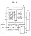
- Figure 1 shows a data processing system containing a scalar unit and a vector unit.
- reference numeral 1′ denotes a scalar unit
- 2′ denotes a vector unit
- 3 denotes a vector execution unit
- 4 and 5 each denote a multiplication and addition pipeline
- 6 denotes a division pipeline
- 7 denotes a vector register
- 8 and 9 each denote a load/store pipeline
- 10 denotes a main storage
- 11 denotes a vector control unit
- 12′ denotes a vector instruction control circuit
- 13 denotes a vector load/store control circuit
- 14′ denotes a memory control unit.
- the scalar unit 1′ fetches instructions in a program in order, executes the fetched instruction when the instruction is a scalar instruction, or sends the fetched instruction to the vector unit 2′ when the instruction is a vector instruction to make the vector unit execute the instruction.
- the vector instruction control circuit 12′ in the vector control unit 11 receives the vector instruction which is transferred from the scalar unit 1′, and controls the execution of the vector instruction.
- the vector instruction is a load instruction or a store instruction
- the execution of the instruction is controlled in the vector load/store control circuit 13, and an operation to access the main storage 10 is carried out through the memory control unit 14′.
- a load operation of vector data which is read from the main storage 10 in the vector register 7 or a store operation of vector data which is read from the vector register 7 in the main storage 10 is carried out in the load/store pipeline 8 or 9 under the control of the vector load/store control circuit 13.
- An operation to access the main storage 10 from the scalar unit 1′ is also carried out through the main storage unit 14′.
- the scalar unit and the vector unit operate in parallel as long as it is possible.
- data which is fetched for an execution of a vector instruction or a scalar instruction is obtained by an execution of a preceding vector instruction or a scalar instruction, the order of operations to access the main storage 10 must be ensured between the preceding instruction and the following instruction.
- the order of operations to access the main storage between a preceding vector load instruction and a following vector instruction, between a preceding vector store instruction and a following vector instruction, between a preceding scalar store instruction and a following vector instruction, between a preceding vector load instruction and a following scalar instruction, and between a preceding vector load instruction and a following scalar instruction are respectively ensured simply regarding the order of obtaining a right of access to the main storage.
- the scalar unit usually contains a buffer memory (cache) for temporarily storing portions (blocks) of data of the main storage to which portions (blocks) the scalar unit has recently accessed.
- a buffer memory for temporarily storing portions (blocks) of data of the main storage to which portions (blocks) the scalar unit has recently accessed.
- serializing operation using a post instruction and a wait instruction is carried out.
- control is performed so that an operation for accessing the main storage for an instruction preceding the post instruction, is carried out before an operation for accessing the main storage for an instruction following the wait instruction.
- no control is performed for the instructions between the post instruction and the wait instruction, regarding the order of operations to access the main storage.
- FIG. 2 shows an example of a sequence of instructions which includes a post instruction and a wait instruction for carrying out a serializing operation.
- POST denotes a post instruction
- WAIT denotes a wait instruction
- LD denotes a scalar load instruction.
- the execution of the scalar load instruction LD which follows the wait instruction, is suspended until a right to access the main storage for the execution of the vector store instruction VST1 which precedes the post instruction POST is obtained.
- Figure 3 shows a typical flow of executions of the vector store instructions VST1 to VST8 of Fig. 2.
- Two vector store instructions are executed simultaneously in parallel in the two load/store pipelines 8 and 9 of Fig. 1.
- the parallelogram for each vector store instruction indicates a plurality of processing flows which are processed in a load/store pipeline.
- an active post pending signal POST-PENDING which indicates whether or not the executions of the vector instructions preceding a post instruction is not completed yet, is output from the vector unit to the scalar unit, the post pending signal POST-PENDING is made active when the execution of the post pending signal POST-PENDING is started in the vector unit, and is made inactive when the executions for all vector instructions preceding the post instruction are completed.
- a wait acknowledge signal WAIT-ACK is output from the vector unit to the scalar unit.
- the scalar unit when a wait instruction is detected, execution of scalar instructions following the wait instruction is first stopped, and the scalar unit awaits the above wait acknowledge signal WAIT-ACK. Then, when the scalar unit receives the wait acknowledge signal WAIT-ACK, the scalar unit determines whether or not the executions for all vector instructions preceding the post instruction are completed, based on the received post pending signal POST-PENDING. When the post pending signal POST-PENDING is inactive, the scalar unit releases the execution of the scalar instructions following the wait instruction, e.g., a scalar load instruction LD shown in Fig. 2 can be executed. Namely, the judgment for the release of scalar instructions following a wait instruction can be made after the wait instruction is started in the vector unit.
- An embodiment of a first aspect of the present invention can provide a data processing system comprising a scalar unit, a vector unit, and a storage.
- the scalar unit receives scalar instructions and vector instructions, carries out scalar data processing in accordance with the scalar instruction, and transfers the vector instruction to the vector unit.
- the vector unit receives the vector instruction from the scalar unit, carries out vector data processing in accordance with the vector instruction, and comprises a post pending signal generating circuit for generating a post pending signal which is made active when a post instruction is received in the vector unit, and is made inactive when a right to access the storage is obtained for reading or storing a last element through operations for all vector instructions preceding the post instruction.
- the scalar unit further comprises, a wait instruction detecting circuit for detecting a transfer of a wait instruction to the vector unit, and an interlock control circuit for suspending executions of instructions which follow a wait instruction which is detected in the wait instruction detecting circuit and each including an operation to access the storage until the post pending signals changes from active to inactive.
- An embodiment of a second aspect of the present invention can provide a data processing system comprising a scalar unit, a vector unit, and a storage.
- the scalar unit receives scalar instructions and vector instructions, carries out scalar data processing in accordance with the scalar instruction, and transfers the vector instruction to the vector unit.
- the vector unit receives the vector instruction from the scalar unit, carries out vector data processing in accordance with the vector instruction, and comprises a first post pending signal generating circuit for generating a first post pending signal which is made active when a post instruction is received from the scalar unit and is made inactive when a right to access the storage is obtained for reading or storing a last element through operations for all vector instructions preceding the post instruction.
- the scalar unit further comprises, a post instruction detecting circuit for detecting a transfer of a post instruction to the vector unit, a wait instruction detecting circuit for detecting a transfer of a wait instruction to the vector unit, a second post pending signal generating circuit which receives the output of the post instruction detecting circuit and the first post pending signal, and generates a second post pending signal which is made active when a post instruction is transferred to the vector unit and is made inactive when the first post pending signal becomes inactive, and an interlock control circuit for suspending executions of instructions which follow the wait instruction which is detected in the wait instruction detecting circuit and each including an operation to access the storage, while the second post pending signal is active.
- An embodiment of a third aspect of the present invention can provide a data processing system comprising a scalar unit, a vector unit, a storage, and a memory control unit.
- the scalar unit receives both a scalar instruction and a vector instruction, carries out scalar data processing in accordance with the scalar instruction, transfers the vector instruction to the vector unit, and sends requests for accessing the storage to the memory control unit during the scalar data processing in accordance with the scalar instruction.
- the vector unit receives the vector instruction from the scalar unit, carries out vector data processing in accordance with the vector instruction, and sends requests for accessing the storage to the memory control unit during the vector data processing in accordance with the vector instruction.
- the memory control unit receives the requests for accessing the storage from the scalar unit and the vector unit, carries out operations to access the storage for the received requests, and comprises a priority control circuit for outputting an active memory access acknowledge signal responding to one of the received requests for giving a right to access the main storage to a corresponding one of the scalar unit and a vector unit.
- the vector unit further comprises a first post pending signal generating circuit for generating a first post pending signal which is made active when a post instruction is received from the scalar unit and is made inactive when a right to access the storage is obtained for reading or storing a last element through operations for all vector instructions preceding the post instruction.
- the scalar unit further comprises, a post instruction detecting circuit for detecting a transfer of a post instruction to the vector unit, a wait instruction detecting circuit for detecting a transfer of a wait instruction to the vector unit, a second post pending signal generating circuit which receives the output of the post instruction detecting circuit and the first post pending signal, and generates a second post pending signal which is made active when a post instruction is transferred to the vector unit and is made inactive when the first post pending signal becomes inactive, and an interlock control circuit for suspending executions of instructions which follow the wait instruction which is detected in the wait instruction detecting circuit and each including an operation to access the storage, while the second post pending signal is active.
- An embodiment of a fourth aspect of the present invention can provide a data processing system comprising a scalar unit, a vector unit, a storage, and a memory control unit.
- the scalar unit receives both a scalar instruction and a vector instruction, carries out scalar data processing in accordance with the scalar instruction, transfers the vector instruction to the vector unit, and requests the memory control unit to access the storage during the scalar data processing in accordance with the scalar instruction.
- the vector unit receives the vector instruction from the scalar unit, carries out vector data processing in accordance with the vector instruction, and sends requests for accessing the storage to the memory control unit during the vector data processing in accordance with the vector instruction.
- the memory control unit receives the requests for accessing the storage from the scalar unit and the vector unit, carries out operations to access the storage for the received requests, and comprises, a buffer memory invalidation address storing circuit for temporarily storing one or more addresses to which addresses in the storage access operations are carried out, a buffer memory invalidation address transferring circuit for transferring the addresses stored in the buffer memory invalidation address storing circuit to the scalar unit, and removing the transferred addresses from the buffer memory invalidation address storing circuit, a transfer complete signal generating circuit for generating a transfer complete signal which indicates that all addresses stored in the buffer memory invalidation address storing circuit have been transferred to the scalar unit when active, and a priority control circuit for outputting an active memory access acknowledge signal responding to one of the received requests for giving a right to access the main storage to a corresponding one of the scalar unit and a vector unit.
- the vector unit further comprises, an after-start stages control circuit for controlling an execution of a vector instruction after its start, including operations to access the storage for a vector instruction, and comprising a last memory access detecting circuit for detecting that a right to access the storage is obtained for reading or storing a last element through the execution of the vector instruction, and outputting a last memory access signal which indicates the detection, and a first post pending signal generating circuit for generating a first post pending signal which is made active when a post instruction is received from the scalar unit, and is made inactive when an active transfer complete signal is received from the memory control unit and an active last memory access signal from the last memory access detecting circuit.
- an after-start stages control circuit for controlling an execution of a vector instruction after its start, including operations to access the storage for a vector instruction, and comprising a last memory access detecting circuit for detecting that a right to access the storage is obtained for reading or storing a last element through the execution of the vector instruction, and outputting a last memory access signal which indicates the
- the scalar unit further comprises, a buffer memory for temporarily storing a portion of data of the main storage, a buffer memory invalidation circuit for invalidating data in the buffer memory using the addresses which are transferred by the buffer memory invalidation address transferring circuit, when the address of the data in the buffer memory corresponds to the address in the storage to which a write operation from the vector unit has been carried out, a post instruction detecting circuit for detecting a transfer of a post instruction to the vector unit, a wait instruction detecting circuit for detecting a transfer of a wait instruction to the vector unit, a second post pending signal generating circuit which receives the output of the post instruction detecting circuit and the first post pending signal, and generates a second post pending signal which is made active when a post instruction is transferred to the vector unit and is made inactive when the first post pending signal becomes inactive, and an interlock control circuit for suspending execution of instructions which follow the wait instruction which is detected in the wait instruction detecting circuit and each including an operation to access the storage, while the second post pending signal is
- the post pending signal which is generated in the post pending signal generating circuit in the vector unit, is made active responding to a reception of a post instruction.
- the interlock control circuit in the scalar unit suspends executions of instructions which follow the wait instruction and each including an operation to access the storage, until the post pending signal changes from active to inactive.
- the post pending signal is made inactive when a right to access the storage is obtained for reading or storing a last element through operations for all vector instructions preceding the post instruction, and receiving the inactive post pending signal, the interlock control circuit in the scalar unit releases the executions of the above instructions which follow the wait instruction in the scalar unit.
- the executions of the above instructions which follow the wait instruction and each including an operation to access the storage can be started as soon as the right to access the storage is obtained for reading or storing a last element through operations for all vector instructions preceding the post instruction.
- the early start of the execution of the instructions following the wait instruction in the scalar unit in parallel with the execution of the vector instructions following the post instruction in the vector unit reduces the total processing time for the successive instructions including a post instruction and a wait instruction.
- the transfer of the post instruction to the vector unit is detected by the post instruction detecting circuit in the scalar unit.
- the second post pending signal generated in the second post pending signal generating circuit in the scalar unit is made active.
- the first post pending signal which is generated in the first post pending signal generating circuit in the vector unit is made active.
- the interlock control circuit in the scalar unit suspends executions of instructions which follow the wait instruction and each including an operation to access the storage, until the second post pending signal changes from active to inactive.
- the first post pending signal is made inactive when a right to access the storage is obtained for reading or storing a last element through operations for all vector instructions preceding the post instruction, and receiving the inactive first post pending signal from the vector unit, the second post pending signal becomes inactive.
- the interlock control circuit in the scalar unit releases the executions of the above instructions which follow the wait instruction and each including an operation to access the storage. Similar to the first aspect of the present invention, the execution of the above instructions which follow the wait instruction and each including an operation to access the storage, can be started as soon as the right to access the storage is obtained for reading or storing a last element through operations for all vector instructions preceding the post instruction.
- the transfer of the post instruction to the vector unit is detected by the post instruction detecting circuit in the scalar unit.
- the second post pending signal generated in the second post pending signal generating circuit in the scalar unit is made active.
- the first post pending signal which is generated in the first post pending signal generating circuit in the vector unit is made active.
- the interlock control circuit in the scalar unit suspends execution of instructions which follow the wait instruction each including an operation to access the storage, until the second post pending signal changes from active to inactive.
- the first post pending signal is made inactive in the vector unit responding to the active memory access acknowledge signal.
- the second post pending signal becomes inactive.
- the interlock control circuit in the scalar unit releases the execution of the above instructions which follow the wait instruction each including an operation to access the storage.
- the execution of the above instructions which follow the wait instruction each including an operation to access the storage can be started as soon as the right to access the storage is obtained for reading or storing a last element through operations for all vector instructions preceding the post instruction.
- the fourth aspect of the present invention covers the data processing system wherein the scalar unit contains a buffer memory.
- the transfer of the post instruction to the vector unit is detected by the post instruction detecting circuit in the scalar unit.
- the second post pending signal generated in the second post pending signal generating circuit in the scalar unit is made active.
- the first post pending signal which is generated in the first post pending signal generating circuit in the vector unit, is made active.
- the interlock control circuit in the scalar unit suspends execution of instructions which follow the wait instruction each including an operation to access the storage, until the second post pending signal changes from active to inactive.
- the obtaining of the right is detected by the last memory access detecting circuit in the vector unit using the memory access acknowledge signal from the memory control unit, and an active last memory access signal is output from the last memory access detecting circuit.
- the address in the storage to which the store operation from the vector unit has been carried out is stored in the buffer memory invalidation address storing circuit, and the address is transferred to the scalar unit by a buffer memory invalidation address transferring circuit.
- the buffer memory invalidation circuit in the scalar unit invalidates data in the buffer memory using the addresses which are transferred by the buffer memory invalidation address transferring circuit, when the address of the data in the buffer memory corresponds to the address in the storage to which the write operation from the vector unit has been carried out.
- the transfer complete signal generating circuit When all addresses stored in the buffer memory invalidation address storing circuit have been transferred to the scalar unit, the transfer complete signal generating circuit generates an active transfer complete signal. When both the last memory access signal and the transfer complete signal become active, the first post pending signal from the first post pending signal generation circuit becomes inactive.
- the second post pending signal becomes inactive.
- the interlock control circuit in the scalar unit releases the execution of the above instructions which follow the wait instruction and each including an operation to access the storage.
- the execution of the above instructions which follow the wait instruction and each including an operation to access the storage can be started as soon as the right to access the storage is obtained for reading or storing a last element through operations for all vector instructions preceding the post instruction.
- Figure 4 shows an outline of the construction of an embodiment of the present invention.
- reference numeral 1 denotes a scalar unit
- 2 denotes a vector unit
- 14 denotes a memory control unit
- 12 denotes a vector instruction control circuit
- 15 denotes a buffer memory
- 16 denotes a post pending signal latch circuit
- 17 denotes a wait pending signal latch circuit
- 18 denotes a buffer invalidation address storage.
- the scalar unit 1, the vector unit 2, the memory control unit 14, and the vector instruction control circuit 12 in the vector unit 2 respectively function basically the same as the corresponding components of Fig. 1, except as explained below.
- the buffer memory 15 in the scalar unit 1 tempo strictlyrarily stores portions (blocks) of data of the main storage to which portions (blocks) the scalar unit has recently accessed.
- the buffer invalidation address storage 18 in the memory control unit 14 temporarily stores addresses in which addresses in the main storage the vector unit 2 has stored data in accordance with vector store instructions when the addresses correspond to the portions of data which is stored in the buffer memory 15 in the scalar unit 1, until the stored addresses are transferred to the scalar unit 1 to invalidate the corresponding portions of data in the buffer memory 15.
- the SERIALIZING START signal is output from the vector instruction control circuit 12 to the buffer invalidation address storage 18, at the timing when the addresses which should be stored in the buffer invalidation address storage 18 for all the vector store instructions preceding a post instruction, have actually been stored in the buffer invalidation address storage 18.
- a BI-PENDING signal is output from the memory control unit 14 to the vector instruction control circuit 12, and is active from the time the memory control unit 14 receives the SERIALIZING START signal until all the the content of the buffer invalidation address storage 18 has been transferred to the scalar unit 1.
- the inversion of the BI-PENDING signal corresponds to the aforementioned transfer complete signal in the fourth aspect of the present invention as explained later.
- the POST-PENDING1 signal which is output from the vector instruction control circuit 12 to the scalar unit 1, is made active when the vector unit 2 receives a post instruction from the scalar unit 1, and is made inactive when the addresses which should be stored in the buffer invalidation address storage 18 for all the vector store instructions preceding a post instruction, have actually been stored in the buffer invalidation address storage 18, and the right to access the storage is obtained for reading or storing a last element through operations for all vector instructions preceding the post instruction.
- the POST-PENDING1 signal corresponds to the aforementioned post pending signal POST-PENDING in the first aspect of the present invention, and the aforementioned first post pending signal in the second to fourth aspects of the present invention.
- the SERIALIZING COMPLETE signal is output from the memory control unit 14 to the scalar unit 1 when the addresses which have been stored in the buffer invalidation address storage 18 for all the vector store instructions preceding a post instruction, have actually been transferred from the buffer invalidation address storage 18 to the scalar unit 1 after the SERIALIZING START signal has been output from the vector instruction control circuit 12 to the buffer invalidation address storage 18.
- the scalar unit 1 suspends the execution of the scalar instructions which follow the wait instruction and which each includes an access operation to the main storage, and carries out an invalidation of the corresponding addresses (blocks) of data in the buffer memory 15.
- Figure 5 shows the construction of the vector unit 2 relating to the present invention.
- 31 denotes a vector instruction fetch stage register
- 32 denotes a post instruction decoder
- 33 denotes a vector instruction fetch stage buffer register
- 34 denotes a vector instruction decode stage register
- 35 denotes a vector instruction start stage buffer register
- 36 denotes a vector instruction start stage register
- 37 denotes an R-stage register
- 38, 40, and 42 each denote an AND circuit
- 39 denotes an S-stage register
- 41 denotes a T-stage register
- 43 denotes a U-stage register
- 100 denotes an instruction start control circuit
- 200 denotes an execution stage control circuit.
- the vector instructions transferred from the scalar unit 1 are held in the vector instruction fetch stage register 31, the vector instruction decode stage register 34, and the vector instruction start stage register 36, respectively, in the corresponding stages.
- the vector instruction fetch stage buffer register 33 is provided between the vector instruction fetch stage register 31 and the vector instruction decode stage register 34
- the vector instruction start stage buffer register 35 is provided between the vector instruction decode stage register 34 and the vector instruction start stage register 36.
- the output of the is decoded in the vector instruction decode stage, and vector instruction decode stage register 34, and the and the vector instruction fetch stage register 31 is decoded, and a post instruction is detected by the post instruction decoder 32.
- the output of the post instruction decoder 32 is attached with a corresponding instruction data as a first post instruction bit "P", and is transferred together with the corresponding instruction data from the vector instruction start stage buffer register 33 through the vector instruction start stage register 36.
- the other bit which is denoted by "V” is a valid bit which indicates whether or not the corresponding stage is valid.
- the instruction start control circuit 100 controls the above operations through the vector instruction fetch stage, the vector instruction decode stage, and the vector instruction start stage.
- the R-stage, S-stage, T-stage, and U-stage are execution control stages of vector instructions, and the execution of each vector instruction in the load/store pipeline is controlled in the above stages.
- the R-stage read stage
- the S-stage start-up stage
- the operation from the start of the execution until the store or load operation of the first element is controlled.
- the T-stage terminal stage
- the operation after the S-stage until the store or load operation of the last element (obtaining of a right to access the main storage for reading or storing a last element through operations for each vector instruction) is controlled.
- exception processing is controlled.
- Each of the R-stage, S-stage, and T-stage registers 37, 39, and 41 contains a valid bit "V” and a second post instruction bit "PF", where the valid bit "V” indicates whether or not the corresponding stage is valid.
- the second post instruction bits "PF" in all of the R-stage, S-stage, and T-stage registers 37, 39, and 41 are made active by the execution stage control circuit 200 when a post instruction is started.
- the execution stage control circuit 200 carries out the setting of the second post instruction bits "PF" responding to a POST-START signal which is supplied from the instruction start control circuit when a post instruction is started.
- Each second post instruction bit "PF" is transferred with the corresponding instruction data through the R-stage, S-stage, and T-stage registers 37, 39, and 41. Namely, when the operation of the vector instruction in the R-stage having an active second post instruction bit "PF" is completed, the operation of the vector instruction is shifted to the S-stage, and the instruction data in the R-stage register 37 is transferred to the S-stage register 39 together with the active second post instruction bit "PF". Similarly, when the operation of the vector instruction in the S-stage having an active second post instruction bit "PF" is completed, the operation of the vector instruction is shifted to the T-stage, and the instruction data in the S-stage register 39 is transferred to the T-stage register 41 together with the active second post instruction bit "PF".
- the valid bit "V” and the second post instruction bit “PF” in the R-stage register 37 are input into the AND circuit 38, the valid bit “V” and the second post instruction bit “PF” in the S-stage register 39 are input into the AND circuit 40, and the valid bit “V” and the second post instruction bit “PF” in the T-stage register 41 are input into the AND circuit 42.
- all the outputs of the AND circuits 38, 40, and 42 become inactive.
- the outputs of the AND circuits 38, 40, and 42 are supplied to the execution stage control circuit 200.
- the execution stage control circuit 200 outputs the SERIALIZING START signal to the memory control unit 14 when all the output of the AND circuits 38, 40, and 42 become inactive and the POST-PENDING1 signal is active.
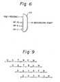
- Figure 6 shows a construction to generate the SERIALIZING START signal in the execution stage control circuit 200.
- Figure 7 shows a construction of the memory control unit 14 relating to the buffer invalidation.
- reference numerals 71, 72, 73, and 74 each denote a port circuit corresponding to one of a plurality of ports which respectively and independently receive one of requests from the scalar unit 1, the vector unit 2, the channel processors, and others, and outputs an acknowledge signal to the unit or the processor which sent the received request, using a priority control circuit (not shown) comprised therein.
- the above port circuits 71, 72, 73, and 74 each comprise a construction for transferring addresses which are to be used for the buffer invalidation, as shown in Fig. 6.
- reference numeral 51 denotes a store address register
- 52 denotes a selector
- 53 denotes a first buffer invalidation register
- 54 denotes a tag register
- 55 denotes a tag storage
- 56 denotes a match detecting circuit
- 57 denotes a second buffer invalidation register
- 58 denotes a match flag register
- 59 denotes a buffer invalidation address storage
- 60 denotes an input pointer
- 61 denotes an output pointer
- 62 denotes a subtraction circuit
- 63 denotes a number register.
- the tag address of the new block is supplied to one of the input terminals of the selector 52, and is written in the tag storage 55 through the tag register 54.
- the address of the main storage to which a store operation is carried out is temporarily held in the store address register 51, and then latched in the first buffer invalidation register 53 through the selector 52.
- the output of the first buffer invalidation register 53 is compared with all the content of the tag storage 55. When a match between the output of the first buffer invalidation register 53 and an tag address in the tag storage 55 is detected, "1" is output from the match circuit 56, and is latched in the match register 58.
- the output of the first buffer invalidation register 53 is then latched in the second buffer invalidation register 57, and the output of the match register 58 is supplied to the buffer invalidation address storage 59 as an input control signal to store the output of the second buffer invalidation register 57 in the buffer invalidation address storage 59.
- the input pointer 60 counts the number of inputs in the buffer invalidation address storage 59
- the output counter 61 counts the number of outputs in the buffer invalidation address storage 59.
- the subtraction circuit 62 subtracts the count of the output counter 61 from the count of the input counter 60.
- the output of the subtraction circuit 62 is latched in the number register 63 when the SERIALIZING START signal is supplied from the execution stage control circuit 200, and the content of the number register 63 is decremented when each of remaining addresses is output from the buffer invalidation address storage 59.
- reference numeral 64 denotes a selector
- 65 denotes a buffer invalidation address register
- 66 denotes a "0" detection circuit.
- the output of the buffer invalidation address storage 59 in the port circuit 71 for the port A is denoted by A′
- similar outputs of buffer invalidation address storages in the port circuits 72, 73, and 74 for the ports B, C, and D are respectively denoted by B′, C′, and D′.
- These outputs A′, B′, C′, and D′ of the buffer invalidation address storages in the port circuits 71, 72, 73, and 74, are input in the selector 64, and are transferred to the scalar unit 1 through the selector 64 and the buffer invalidation address register 65.
- the output of the number register 63 in the port circuit 71 for the port A is denoted by A ⁇
- similar outputs of number registers in the port circuits 72, 73, and 74 for the ports B, C, and D are respectively denoted by B ⁇ , C ⁇ , and D ⁇ . All the outputs A ⁇ , B ⁇ , C ⁇ , and D ⁇ of the number registers are applied to the "0" detection circuit 66.
- the "0" detection circuit 66 determines whether or not all the outputs A ⁇ , B ⁇ , C ⁇ , and D ⁇ are zero, and outputs the BI-PENDING signal which is "0" when all the outputs A ⁇ , B ⁇ , C ⁇ , and D ⁇ are zero, i.e., all addresses stored in the buffer invalidation address storages in the port circuits 71, 72, 73, and 73 have been transferred to the execution stage control circuit 200.
- the "0" detection circuit 66 also outputs the SERIALIZING COMPLETE signal through the buffer invalidation address register 65 to the scalar unit 1.
- Figure 8 shows a construction for generating the POST-PENDING1 signal in the execution stage control circuit 200.
- reference numerals 81, 82, 83, 84, and 85 each denote an AND circuit
- 86 denotes an OR circuit
- 201 denotes the other portion of the execution stage control circuit 200.
- VFS-VALID denotes the output of the valid bit of the vector instruction fetch stage register 31
- VFB-VALID denotes the output of the valid bit of the vector instruction fetch stage buffer register 33
- VPS-VALID denotes the output of the valid bit of the vector instruction decode stage register 34
- VQB-VALID denotes the output of the valid bit of the vector instruction start stage buffer register 35
- VQS-VALID denotes the output of the valid bit of the vector instruction start stage register 36.
- VFS-POST-INST denotes the output of the post instruction bit of the vector instruction fetch stage register 31
- VFB-POST-INST denotes the output of the post instruction bit of the vector instruction fetch stage buffer register 33
- VPS-POST-INST denotes the output of the post instruction bit of the vector instruction decode stage register 34
- VQB-POST-INST denotes the output of the post instruction bit of the vector instruction start stage buffer register 35
- VQS-POST-INST denotes the output of the post instruction bit of the vector instruction start stage register 36.
- the above VFS-VALID signal and the above VFS-POST-INST signal are input into the AND circuit 81
- the above VFB-VALID signal and the above VFB-POST-INST signal are input into the AND circuit 82
- the above VPS-VALID signal and the above VPS-POST-INST signal are input into the AND circuit 83
- the above VQB-VALID signal and the above VQO-POST-INST signal are input into the AND circuit 84
- the above VQS-VALID signal and the above VQS-POST-INST signal are input into the AND circuit 85.
- All the outputs of the AND circuits 81 to 85 and a POST-PENDING0 signal from the circuit 201 are input in the OR circuit 86.
- the POST-PENDING0 signal is generated in the circuit 201 as a logical sum of the BI-PENDING signal and all the outputs of the AND circuits 38, 40, and 42.
- the OR circuit 86 outputs the POST-PENDING1 signal which is supplied to the scalar unit 1.
- the POST-PENDING1 signal is active when a post instruction is held in any of the vector instruction fetch stage register 31, the vector instruction fetch stage buffer register 33, the vector instruction decode stage register 34, the vector instruction start stage buffer register 35, and the vector instruction start stage register 36, or when a right to access the storage has not been obtained for reading or storing a last element through operations for all vector instructions preceding the post instruction, or when an address stored in the buffer memory invalidation address storing circuit has not been transferred to the scalar unit yet.
- a scalar instruction is processed in a plurality of processing flows by pipeline processing, and generally each flow comprises a decode stage D, an address calculation stage A, an address transformation stage T, a buffer access stage B, an execution stage E, and a write stage W for writing a result of the execution.
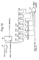
- Figure 10 shows a construction for generating a POST-PENDING2 signal in the scalar unit 1.
- reference numerals 91, 101, 102, 103, and 104 each denote an AND circuit
- 92 denotes an RS-type flip-flop circuit
- 93 to 99 each denote a register
- 105 denotes a NOR circuit.
- the POST-INST signal shown in Fig. 10 is generated by decoding an instruction which is newly fetched in the scalar unit 1, although the decoder is not shown.
- the WAIT-INST signal becomes active when a post instruction is detected in the decoder.
- the A rel signal is a A-stage release signal which is output from a control circuit (not shown) of the scalar unit 1, which controls the pipeline processing in the scalar unit 1, when an execution of a scalar instruction is released from the A-stage (the address calculation stage as mentioned before with reference to Fig. 9).
- T rel , B rel , and E rel signals are respectively release signals from the T-stage, B-stage, and E-stage (Fig. 9)
- T val , B val , E val , and W val signals are respectively valid signals of the T-stage, B-stage, E-stage, and W-stage (Fig. 9).
- the POST-INST signal and the A rel signal are input into the AND circuit 91, and the output of the AND circuit 91 is applied to the set input terminal S of the flip-flop circuit 92.
- the post instruction is detected by the above-mentioned decoder, and the POST-INST signal becomes active.
- the A rel signal becomes active, and thus the flip-flop circuit 92 is set to make its Q-output active.
- the Q-output of the flip-flop circuit 92 is the above POST-PENDING2 signal.
- the output of the AND circuit 91 is also applied to the register 93, and is input into the register 93 synchronized with a clock when the above A rel signal is active.
- the output of the register 93 is applied to the register 94, and is input into the register 94 synchronized with the clock when the above T rel signal is active.
- the output of the register 94 is applied to the register 95, and is input into the register 95 synchronized with the clock when the above B rel signal is active.
- the output of the register 95 is applied to the register 96, and is input into the register 96 synchronized with the clock when the above E rel signal is active.
- Three further registers 97, 98, and 99 are provided following the above registers 93 to 96.
- the output of the registers 93, 94, 95, and 96 are respectively applied to input terminals of each of the AND circuits 101, 102, 103, and 104, and the above T val , B val , E val , and W val signals are respectively applied to other input terminals of the AND circuits 101, 102, 103, and 104.
- the outputs of the AND circuits 101, 102, 103, and 104, the output of the registers 97 to 99, and the POST-PENDING1 signal from the vector unit 2 are input into the NOR circuit 105, and the output of the NOR circuit 105 is applied to the flip-flop circuit 92 as a reset signal RESET-POST-PENDING.
- the outputs of the AND circuits 101 to 104 respectively indicate whether or not a post instruction is processed in the respective stages of the pipeline in the scalar unit 1.
- the POST-PENDING2 signal becomes active when a post instruction is released from the A-stage of the pipeline in the scalar unit 1, and is maintained until the POST-PENDING1 signal from the vector unit 2 becomes inactive.
- the above three registers 97 to 99 are provided for maintaining the activeness of the POST-PENDING2 signal after the post instruction is released from the W-stage of the scalar unit 1 until the POST-PENDING1 signal from the vector unit 2 becomes active responding to a reception of the post instruction by the vector unit 2.
- Figure 11 shows a construction for generating an INTERLOCK signal in the scalar unit 1.
- reference numerals 111, 112, and 114 each denote an AND circuit, and 113 denotes an RS-type flip-flop circuit.
- the WAIT-INST signal and the ACCESS-INST signal shown in Fig. 11 are generated by decoding an instruction which is newly fetched in the scalar unit 1, although the decoder is not shown.
- the WAIT-INST signal becomes active when a wait instruction is detected in the decoder, and the ACCESS-INST signal becomes active when a scalar instruction whose operation includes an access operation to the main storage, is detected in the decoder.
- the A rel signal is the aforementioned A-stage release signal which is output when an execution of a scalar instruction is released from the A-stage.
- the POST-PENDING2 signal, the WAIT-INST signal, and the A rel signal are input into the AND circuit 111, and the output of the AND circuit 111 is applied to the set input terminal S of the flip-flop circuit 113.
- the output of the AND circuit 111 is active when a wait instruction is released from the A-stage and the POST-PENDING2 signal is active.
- the Q-output of the flip-flop circuit 113 is denoted by a WAIT-PENDING, and is applied to one input terminal of each of the AND circuits 112 and 114.
- the inversion of the POST-PENDING2 signal is applied to the other input terminal of the AND circuit 112.
- the output of the AND circuit 112 is applied to the reset input terminal of the flip-flop circuit 113.
- the ACCESS-INST signal is applied to the other input terminal of the AND circuit 114.
- the output of the AND circuit 114 is obtained as the INTERLOCK signal which is a control signal to suspend execution of scalar instructions which follow the wait instruction and whose operation includes an access operation to the main storage.
- the flip-flop circuit 113 is set, i.e., the WAIT-PENDING signal becomes active.
- the WAIT-PENDING signal becomes active
- the INTERLOCK signal becomes active when a scalar instruction which follows the wait instruction and whose operation includes an access operation to the main storage, is detected. Therefore, the execution of the scalar instruction as above, is suspended.
- FIG. 12A to 12C shows an example of the operations of the embodiment of the present invention.
- Figs. 12A to 12C the operations in the scalar unit 1 are shown in the upper half area SU of Figs. 12A to 12C, the operations in the vector unit 2 are shown in the lower half area VU of Figs. 12A to 12C, the operations a post instruction and a wait instruction are respectively executed in four flows of operations through a pipeline in the scalar unit 1, as explained before with reference to Fig. 9, and active signals and valid stages of the operations are respectively indicated by solid lines.
- the POST-PENDING2 signal When an A rel signal for a post instruction is output from the aforementioned control circuit, the POST-PENDING2 signal becomes active, and the activeness of the POST-PENDING2 signal is maintained by itself until three cycles (3 ⁇ ) elapse after the W-stage operation for the post instruction is completed in the scalar unit 1.
- the instruction data of the post instruction is transferred to the vector unit 2 in four cycles which are denoted by IV and DV.
- the vector unit 2 Responding to the first cycle of the transfer IV, the vector unit 2 detects the reception of the post instruction, the POST-PENDING1 signal becomes active, and the active POST-PENDING1 signal maintains the above activeness of the POST-PENDING2 signal in the scalar unit 1.
- Figure 12C shows an operation when the POST-PENDING2 signal is inactive when a wait instruction is released from the A-stage.
- the WAIT-PENDING signal is inactive, i.e., the INTERLOCK signal is inactive, and therefore, the execution of the scalar instruction following the wait instruction is immediately started.
Landscapes
- Engineering & Computer Science (AREA)
- Theoretical Computer Science (AREA)
- Software Systems (AREA)
- General Engineering & Computer Science (AREA)
- Physics & Mathematics (AREA)
- General Physics & Mathematics (AREA)
- Complex Calculations (AREA)
- Advance Control (AREA)
Applications Claiming Priority (2)
| Application Number | Priority Date | Filing Date | Title |
|---|---|---|---|
| JP1121277A JP2677414B2 (ja) | 1989-05-15 | 1989-05-15 | 命令実行のシリアライズ制御方式 |
| JP121277/89 | 1989-05-15 |
Publications (3)
| Publication Number | Publication Date |
|---|---|
| EP0398639A2 true EP0398639A2 (fr) | 1990-11-22 |
| EP0398639A3 EP0398639A3 (fr) | 1991-05-29 |
| EP0398639B1 EP0398639B1 (fr) | 1996-09-18 |
Family
ID=14807272
Family Applications (1)
| Application Number | Title | Priority Date | Filing Date |
|---|---|---|---|
| EP90305212A Expired - Lifetime EP0398639B1 (fr) | 1989-05-15 | 1990-05-15 | Opération de mise en série d'une instruction vecteur et d'une instruction scalaire dans un système de traitement de données |
Country Status (5)
| Country | Link |
|---|---|
| US (1) | US5247691A (fr) |
| EP (1) | EP0398639B1 (fr) |
| JP (1) | JP2677414B2 (fr) |
| CA (1) | CA2016532C (fr) |
| DE (1) | DE69028572T2 (fr) |
Cited By (2)
| Publication number | Priority date | Publication date | Assignee | Title |
|---|---|---|---|---|
| EP0529303A3 (en) * | 1991-08-29 | 1993-09-22 | International Business Machines Corporation | Checkpoint synchronization with instruction overlap enabled |
| EP0600583A1 (fr) * | 1992-11-30 | 1994-06-08 | Fujitsu Limited | Processeur vectoriel |
Families Citing this family (21)
| Publication number | Priority date | Publication date | Assignee | Title |
|---|---|---|---|---|
| US5530881A (en) * | 1991-06-06 | 1996-06-25 | Hitachi, Ltd. | Vector processing apparatus for processing different instruction set architectures corresponding to mingled-type programs and separate-type programs |
| US5809552A (en) * | 1992-01-29 | 1998-09-15 | Fujitsu Limited | Data processing system, memory access device and method including selecting the number of pipeline stages based on pipeline conditions |
| US5872988A (en) * | 1992-06-17 | 1999-02-16 | U.S. Philips Corporation | Parallel data processing device having a concatenated data path between elementary processors |
| US6513107B1 (en) | 1999-08-17 | 2003-01-28 | Nec Electronics, Inc. | Vector transfer system generating address error exception when vector to be transferred does not start and end on same memory page |
| US6625720B1 (en) * | 1999-08-17 | 2003-09-23 | Nec Electronics, Inc. | System for posting vector synchronization instructions to vector instruction queue to separate vector instructions from different application programs |
| US6857061B1 (en) | 2000-04-07 | 2005-02-15 | Nintendo Co., Ltd. | Method and apparatus for obtaining a scalar value directly from a vector register |
| US20030196072A1 (en) * | 2002-04-11 | 2003-10-16 | Chinnakonda Murali S. | Digital signal processor architecture for high computation speed |
| US7577816B2 (en) * | 2003-08-18 | 2009-08-18 | Cray Inc. | Remote translation mechanism for a multinode system |
| US7519771B1 (en) | 2003-08-18 | 2009-04-14 | Cray Inc. | System and method for processing memory instructions using a forced order queue |
| US7743223B2 (en) * | 2003-08-18 | 2010-06-22 | Cray Inc. | Decoupling of write address from its associated write data in a store to a shared memory in a multiprocessor system |
| US8307194B1 (en) | 2003-08-18 | 2012-11-06 | Cray Inc. | Relaxed memory consistency model |
| US7543133B1 (en) | 2003-08-18 | 2009-06-02 | Cray Inc. | Latency tolerant distributed shared memory multiprocessor computer |
| US7437521B1 (en) * | 2003-08-18 | 2008-10-14 | Cray Inc. | Multistream processing memory-and barrier-synchronization method and apparatus |
| US7421565B1 (en) | 2003-08-18 | 2008-09-02 | Cray Inc. | Method and apparatus for indirectly addressed vector load-add -store across multi-processors |
| US7478769B1 (en) | 2005-03-09 | 2009-01-20 | Cray Inc. | Method and apparatus for cooling electronic components |
| US20070074008A1 (en) * | 2005-09-28 | 2007-03-29 | Donofrio David D | Mixed mode floating-point pipeline with extended functions |
| US7694025B1 (en) | 2006-03-31 | 2010-04-06 | Integrated Device Technology, Inc. | Method and device for base address sorting and entry into base address registers |
| US7647438B1 (en) | 2006-05-09 | 2010-01-12 | Integrated Device Technology, Inc. | Binary base address sorting method and device with shift vector |
| US7779197B1 (en) | 2006-05-09 | 2010-08-17 | Integrated Device Technology, Inc. | Device and method for address matching with post matching limit check and nullification |
| US7634586B1 (en) | 2006-06-05 | 2009-12-15 | Integrated Device Technology, Inc. | Device for concurrent limit validity check |
| CN115185867B (zh) * | 2022-03-24 | 2026-03-03 | 海光信息技术股份有限公司 | 处理访问请求的方法 |
Family Cites Families (8)
| Publication number | Priority date | Publication date | Assignee | Title |
|---|---|---|---|---|
| JPS6043535B2 (ja) * | 1979-12-29 | 1985-09-28 | 富士通株式会社 | 情報処理装置 |
| JPS6186844A (ja) * | 1984-10-04 | 1986-05-02 | Fujitsu Ltd | 逐次化命令の移動方式 |
| JPS6224366A (ja) * | 1985-07-03 | 1987-02-02 | Hitachi Ltd | ベクトル処理装置 |
| US4760518A (en) * | 1986-02-28 | 1988-07-26 | Scientific Computer Systems Corporation | Bi-directional databus system for supporting superposition of vector and scalar operations in a computer |
| JPH06103494B2 (ja) * | 1986-11-18 | 1994-12-14 | 株式会社日立製作所 | ベクトル処理装置の制御方式 |
| JPS63253468A (ja) * | 1987-04-10 | 1988-10-20 | Hitachi Ltd | ベクトル処理装置 |
| JPS6432379A (en) * | 1987-07-29 | 1989-02-02 | Hitachi Ltd | Computer |
| JPS6467680A (en) * | 1987-09-09 | 1989-03-14 | Hitachi Ltd | Vector processor |
-
1989
- 1989-05-15 JP JP1121277A patent/JP2677414B2/ja not_active Expired - Lifetime
-
1990
- 1990-05-10 CA CA002016532A patent/CA2016532C/fr not_active Expired - Fee Related
- 1990-05-15 EP EP90305212A patent/EP0398639B1/fr not_active Expired - Lifetime
- 1990-05-15 DE DE69028572T patent/DE69028572T2/de not_active Expired - Fee Related
- 1990-05-15 US US07/523,567 patent/US5247691A/en not_active Expired - Fee Related
Cited By (5)
| Publication number | Priority date | Publication date | Assignee | Title |
|---|---|---|---|---|
| EP0529303A3 (en) * | 1991-08-29 | 1993-09-22 | International Business Machines Corporation | Checkpoint synchronization with instruction overlap enabled |
| US5495587A (en) * | 1991-08-29 | 1996-02-27 | International Business Machines Corporation | Method for processing checkpoint instructions to allow concurrent execution of overlapping instructions |
| US5495590A (en) * | 1991-08-29 | 1996-02-27 | International Business Machines Corporation | Checkpoint synchronization with instruction overlap enabled |
| EP0600583A1 (fr) * | 1992-11-30 | 1994-06-08 | Fujitsu Limited | Processeur vectoriel |
| US5574924A (en) * | 1992-11-30 | 1996-11-12 | Fujitsu Limited | Vector processing device that utilizes post marks to ensure serialization of access requests of vector store instructions |
Also Published As
| Publication number | Publication date |
|---|---|
| EP0398639A3 (fr) | 1991-05-29 |
| JPH02300852A (ja) | 1990-12-13 |
| EP0398639B1 (fr) | 1996-09-18 |
| CA2016532C (fr) | 1994-04-26 |
| US5247691A (en) | 1993-09-21 |
| DE69028572T2 (de) | 1997-01-30 |
| CA2016532A1 (fr) | 1990-11-15 |
| JP2677414B2 (ja) | 1997-11-17 |
| DE69028572D1 (de) | 1996-10-24 |
Similar Documents
| Publication | Publication Date | Title |
|---|---|---|
| EP0398639B1 (fr) | Opération de mise en série d'une instruction vecteur et d'une instruction scalaire dans un système de traitement de données | |
| US5293500A (en) | Parallel processing method and apparatus | |
| US5404552A (en) | Pipeline risc processing unit with improved efficiency when handling data dependency | |
| JP3778573B2 (ja) | データプロセッサ及びデータ処理システム | |
| JP2741594B2 (ja) | I/oプロセツサ用の実行装置 | |
| US4949241A (en) | Microcomputer system including a master processor and a slave processor synchronized by three control lines | |
| EP0213842A2 (fr) | Mécanisme de recherche de données en mémoire en parallèle avec l'exécution d'instructions dans un processeur à jeu d'instructions réduit | |
| EP0125855B1 (fr) | Système de commande de mémoire tampon | |
| JP2008515096A (ja) | 複数のコアを介してのモニタリングされたキャッシュラインの共有 | |
| US5961633A (en) | Execution of data processing instructions | |
| US5497496A (en) | Superscalar processor controlling fetching of instructions based upon number of empty instructions registers detected for each cycle | |
| US4631668A (en) | Storage system using comparison and merger of encached data and update data at buffer to cache to maintain data integrity | |
| CA2497807A1 (fr) | Dispositif de traitement vectoriel avec fonction de depassement | |
| US5226166A (en) | Parallel operation processor with second command unit | |
| WO1996027833A1 (fr) | Unite de traitement informatique | |
| KR880001418B1 (ko) | 데이터 처리장치 | |
| EP0223150B1 (fr) | Dispositif de traitement d'information | |
| US6738837B1 (en) | Digital system with split transaction memory access | |
| EP0227319A2 (fr) | Antémémoire d'instructions | |
| US5742842A (en) | Data processing apparatus for executing a vector operation under control of a master processor | |
| US5586336A (en) | Microcomputer capable of monitoring internal resources from external | |
| CA1208798A (fr) | Dispositif de controle du temps pour processeur de donnees | |
| EP0333231B1 (fr) | Système micro-ordinateur pouvant accéder à une mémoire à vitesse élevée | |
| EP0318702A2 (fr) | Processeur de données à transfert direct de données entre le coprocesseur et la mémoire | |
| US7143247B1 (en) | Method and apparatus for parallel execution pipeline data storage in a computer memory |
Legal Events
| Date | Code | Title | Description |
|---|---|---|---|
| PUAI | Public reference made under article 153(3) epc to a published international application that has entered the european phase |
Free format text: ORIGINAL CODE: 0009012 |
|
| AK | Designated contracting states |
Kind code of ref document: A2 Designated state(s): DE FR GB |
|
| PUAL | Search report despatched |
Free format text: ORIGINAL CODE: 0009013 |
|
| AK | Designated contracting states |
Kind code of ref document: A3 Designated state(s): DE FR GB |
|
| 17P | Request for examination filed |
Effective date: 19911120 |
|
| 17Q | First examination report despatched |
Effective date: 19940426 |
|
| GRAH | Despatch of communication of intention to grant a patent |
Free format text: ORIGINAL CODE: EPIDOS IGRA |
|
| GRAH | Despatch of communication of intention to grant a patent |
Free format text: ORIGINAL CODE: EPIDOS IGRA |
|
| GRAA | (expected) grant |
Free format text: ORIGINAL CODE: 0009210 |
|
| AK | Designated contracting states |
Kind code of ref document: B1 Designated state(s): DE FR GB |
|
| REF | Corresponds to: |
Ref document number: 69028572 Country of ref document: DE Date of ref document: 19961024 |
|
| ET | Fr: translation filed | ||
| PLBE | No opposition filed within time limit |
Free format text: ORIGINAL CODE: 0009261 |
|
| STAA | Information on the status of an ep patent application or granted ep patent |
Free format text: STATUS: NO OPPOSITION FILED WITHIN TIME LIMIT |
|
| 26N | No opposition filed | ||
| PGFP | Annual fee paid to national office [announced via postgrant information from national office to epo] |
Ref country code: GB Payment date: 20000510 Year of fee payment: 11 Ref country code: FR Payment date: 20000510 Year of fee payment: 11 |
|
| PGFP | Annual fee paid to national office [announced via postgrant information from national office to epo] |
Ref country code: DE Payment date: 20000515 Year of fee payment: 11 |
|
| PG25 | Lapsed in a contracting state [announced via postgrant information from national office to epo] |
Ref country code: GB Free format text: LAPSE BECAUSE OF NON-PAYMENT OF DUE FEES Effective date: 20010515 |
|
| GBPC | Gb: european patent ceased through non-payment of renewal fee |
Effective date: 20010515 |
|
| PG25 | Lapsed in a contracting state [announced via postgrant information from national office to epo] |
Ref country code: FR Free format text: LAPSE BECAUSE OF NON-PAYMENT OF DUE FEES Effective date: 20020131 |
|
| PG25 | Lapsed in a contracting state [announced via postgrant information from national office to epo] |
Ref country code: DE Free format text: LAPSE BECAUSE OF NON-PAYMENT OF DUE FEES Effective date: 20020301 |