EP0400612A2 - Automate programmable - Google Patents
Automate programmable Download PDFInfo
- Publication number
- EP0400612A2 EP0400612A2 EP90110272A EP90110272A EP0400612A2 EP 0400612 A2 EP0400612 A2 EP 0400612A2 EP 90110272 A EP90110272 A EP 90110272A EP 90110272 A EP90110272 A EP 90110272A EP 0400612 A2 EP0400612 A2 EP 0400612A2
- Authority
- EP
- European Patent Office
- Prior art keywords
- input
- result
- program
- section
- delay element
- Prior art date
- Legal status (The legal status is an assumption and is not a legal conclusion. Google has not performed a legal analysis and makes no representation as to the accuracy of the status listed.)
- Withdrawn
Links
Images


Classifications
-
- G—PHYSICS
- G05—CONTROLLING; REGULATING
- G05B—CONTROL OR REGULATING SYSTEMS IN GENERAL; FUNCTIONAL ELEMENTS OF SUCH SYSTEMS; MONITORING OR TESTING ARRANGEMENTS FOR SUCH SYSTEMS OR ELEMENTS
- G05B19/00—Program-control systems
- G05B19/02—Program-control systems electric
- G05B19/04—Program control other than numerical control, i.e. in sequence controllers or logic controllers
- G05B19/05—Programmable logic controllers, e.g. simulating logic interconnections of signals according to ladder diagrams or function charts
- G05B19/058—Safety, monitoring
-
- G—PHYSICS
- G05—CONTROLLING; REGULATING
- G05B—CONTROL OR REGULATING SYSTEMS IN GENERAL; FUNCTIONAL ELEMENTS OF SUCH SYSTEMS; MONITORING OR TESTING ARRANGEMENTS FOR SUCH SYSTEMS OR ELEMENTS
- G05B2219/00—Program-control systems
- G05B2219/10—Plc systems
- G05B2219/13—Plc programming
- G05B2219/13175—For each input corresponding delay time for output response
-
- G—PHYSICS
- G05—CONTROLLING; REGULATING
- G05B—CONTROL OR REGULATING SYSTEMS IN GENERAL; FUNCTIONAL ELEMENTS OF SUCH SYSTEMS; MONITORING OR TESTING ARRANGEMENTS FOR SUCH SYSTEMS OR ELEMENTS
- G05B2219/00—Program-control systems
- G05B2219/10—Plc systems
- G05B2219/13—Plc programming
- G05B2219/13186—Simulation, also of test inputs
Definitions
- the present invention relates to a programmable controller that simulates program runs by use of simulated inputs.
- the programmable controller is connected to such input devices as sensors and limit switches as well as to external loads such as valves and motors to be controlled.
- the steps to control the target equipment are compiled beforehand as a program that is incorporated in the controller.
- Fig. 16 (a) shows a prior art example of simulating program runs with a programmable controller.
- a programmable controller 1 is connected to an external load (device) 3 and to a limit switch 2a that runs in conjunction with the load.
- a driving output signal from the programmable controller 1 activates the external load 3.
- the limit switch 2a operates a certain period of time after the starting of the operation. Instead of having these actions actually carried out, which can be dangerous because of the unpredictability involved, the arrangement in Fig. 16 uses an externally prepared input switch for testing 2′ that is manually operated for program simulation by use of the programmable controller alone.
- a prior art solution to this problem is to incorporate the input switch for testing 2′ in the programmable controller, as disclosed in Japanese Patent Laid-open No. 56-85104.
- Another prior art solution is to program beforehand the number of the input switch to be tested and to refer to the number during simulation, as disclosed in Japanese Patent Laid-open No. 63-21900. The latter setup eliminates the need for the input switch for testing.
- an input section admits input information about the target load to be controlled.
- the memory stores a sequence program. Connected to these components, the CPU carries out operations in accordance with the sequence program.
- the delay element connected to the CPU, has a predetermined delay time set thereto. During simulation, the result of the operation by the CPU is turned into an input signal that takes on the delay time when passing through the delay element before the signal is fed back to the CPU.
- the delay element has an ability to count not the delay time but the time that has elapsed since the CPU gave the result of its operation. A comparison is made between the elapsed time counted by the delay element on the one hand, and the delay time established in a simulated input program in memory on the other. At the proper timings based on the comparison, the current result of the operation by the CPU is regarded as an appropriate input signal that is fed back to the CPU.
- the delay element provides the operational result it received with the delay time that was set during simulation, and feeds back the outcome thereof to the CPU. Using its counting ability, the delay element compares the time it counted with the delay time established in the simulated input program. At the proper timings, the current operational result is fed back to the CPU. In this manner, the proper delay timings can be set for simulation purposes.
- Fig. 1 is a block diagram showing the entire construction of the first embodiment.
- reference numeral 1 is a programmable controller
- numerals 2a, 2b, ... 2n are a plurality of external input devices (i.e., objects to be controlled)
- numeral 4 is an input section that removes the chattering and other disturbances from each of a plurality of input signals (i.e., input information) coming from the external input devices
- numeral 6 is a CPU (central processing unit) that performs operations according to the contents of a sequence program
- numeral 5 is an output section that informs an external load 3 of the result of the operation by the CPU.
- Reference numeral 7 is a user RAM (memory) that contains beforehand the sequence program and a simulated input program.
- Numeral 8 is a ROM (read only memory) that comprises a system program for comprehensive control over the above-mentioned parts.
- Numerals 9 and 10 are a delay circuit (element) and an OR gate, respectively; they are each provided as many as the external input devices installed.
- the delay circuit 9 comprises a latch element 11 that has a control signal line 15 connected to the CPU, a select signal line 14 and a data bus 16 through which the result of the operation (e.g., input number, delay time) by the CPU 6 is stored into the element 11.
- An AND gate 12 receives via a signal line 17 the output of the latch 11 and a pulse signal from an oscillator, not shown. The AND'ed output is used by the CPU 6 to set beforehand delay time data in a counter 13 by way of the data bus 16. The delay time data is decremented by 1 until the data reaches "0". At this point, a high-level signal "1" is output to a delay time output signal line 18. At the same time, decrementing of the counter is stopped.
- the delay time output signal line 18 is connected to a terminal of the OR gate 10.
- Fig. 2 is a block diagram of an attached circuit 19 shown in Fig. 1.
- reference numeral 61 is a program counter for specifying a desired address in the user memory 7
- numeral 62 is a latch that stores the contents (an operation code comprising an instruction and an I/O number) read from the user memory 7
- numeral 63 is a decoder for decoding the instruction part
- numeral 64 is a decoder for decoding the I/O number part
- numeral 65 is a latch that stores delay time data.
- Fig. 3 shows part of the contents of the user RAM 7.
- the contents comprise the simulated input program for generating simulated inputs during simulation, and the sequence program for actually executing and simulating the sequence involved.
- Fig. 3 (a) partially depicts the contents of the addresses in the user RAM 7, and
- Fig. 3 (b) illustrates the contents thereof in ladder format.
- those parts of the simulated input program which are enclosed with an elongated circle each e.g., X10, 0.5
- X10 is an input number
- 0.5 is a delay time.
- Fig. 4 defines the contents of Fig. 3 (a).
- the addresses 1002, 1003, 1005 and 1006 in Fig. 3(a) are of the format shown in Fig. 4 (a); the addresses 1001 and 1004 are of the format depicted in Fig. 4 (b).
- the LOAD and OUT I in Fig. 3 (a) are an instruction code each; Y50 and Y51 are output numbers; 10.03 is an input number; and 0.5 and 0.03 are delay time data.
- Fig. 4 (a) shows the part which creates the simulated input of the simulated input program, comprised of two words or four bytes.
- Fig. 4 (b) depicts part of the simulated input program and the construction of each of the instructions in the sequence program.
- step 100 power is applied in step 100.
- the system is initialized in step 101 and each output is turned off (i.e., "0" output).
- step 102 the program counter 61 (Fig. 2) is initialized, which allows the start address of the user memory 7 (address 1001 in Fig. 3) to be specified.
- step 103 the contents of the user memory (operation code at address 1001) are read and operated on. Because its operation code is LOAD Y50, this instruction specifies that the on/off ("1" or "0") information of output N050 be read out. This causes the process of Fig. 6 is to be carried out. As shown in Fig. 6, the result (i.e., contents of Y50) that was read out is stored in step 107 into a register ACC that the CPU 6 possesses.
- step 104 a check is made in step 104 to see if the above-described processing is ended. If the processing is not ended, the program counter 61 is incremented in step 105 in order to read the contents of the next address (e.g., address 1002) in the user memory.
- the next address e.g., address 1002
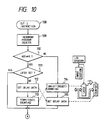
- the operation code at address 1002 is found to be OUT I, 10, 0.5, which causes the OUT I instruction to be executed as per the flow in Fig. 10.
- the OUT I instruction is defined as an instruction that outputs an ON level following a period of time reflecting the stored delay time (0.5) if the result of the operation so far (i.e., contents stored in ACC) is at the ON ("1") level. Specifically, this instruction is executed as follows.
- step 109 the program counter 61 is incremented and the delay time data (0.5) is read from address 1003 of Fig. 3.
- step 110 a check is made on the contents of the ACC. If the result is "1", the processing goes to step 111.
- step 111 another check is made to see if the latch is set. If the latch is not set, the delay time data (0.5) that was read earlier is set to the counter 13 of Fig. 1 in step 112.
- step 113 the latch 11 is ordered to allow the decrementing to take place.
- step 111 If the latch is found set in step 111, nothing is done and process A of Fig. 5 is reached.
- step 110 If the contents of the ACC are found to be "0" in step 110, the latch 11 is ordered to inhibit the decrementing in step 114. The delay time data that was read out earlier is then set to the counter 13. With the delay time output signal line 18 set to "0" (turned off), the processing of Fig. 10 comes to an end.
- the on/off state of Y50 in step 1001 of the simulated input program is an outcome of the output of Y50 in the sequence program of the same figure in ladder format.
- the two kinds of Y50 in the two programs provide the relationship between the external load 3 and the contact 2a (limit switch) associated therewith in Fig. 16.
- Figs. 7, 8 and 9 illustrate other examples of how step 103 of Fig. 5 is carried out with the AND, OR and OUT instructions, respectively.
- the delay time is determined by the width of reference pulses generated by a pulse source (oscillator), not shown, from which the signal line 17 originates in Fig. 1.
- the delay time is set for 0.1 sec.
- the time may be set for 0.01 sec., 1 sec., etc. so as to vary the maximum delay time involved.
- the delay time data is set for "0"
- the result of the operation by the CPU may be given as an input with no delay time.
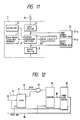
- Figs. 11 and 12 what differs from Fig. 1 is the inclusion of a delay circuit 20 (delay element) and a storage section 21 that stores the result of the input signal output.
- a specific construction of the delay circuit 20 is shown in Fig. 12.
- FIGs. 1 and 12 like reference characters designate like or corresponding parts.
- Reference numeral 22 is a three-state buffer to which the result counted by the counter 13 after the delay time is output.
- input signals from all external input devices are admitted by the system program through the input section 4 and the CPU 6 for storage into an input signal storage area 21-a of the storage section 21.
- the second embodiment has as many delay circuits 20 as the number of inputs.
- the difference in this respect between the first and the second embodiment is that, as shown in Fig. 12, the result counted by the counter 13 after the delay time is read to the CPU 6 via the three-state buffer 21 and the data bus 16, the CPU thereafter outputting the result to the input signal storage area 21-a. That is, whereas the output from the delay circuit 9 is returned to the OR gate 10 in the first embodiment, the output therefrom in the second embodiment is returned via the CPU 6 to the input signal storage area 21-a.
- the third embodiment involves having input signals from all external input devices stored via the CPU into an input signal storage area 25-a of a storage section 25.
- a single time counting section 26 is provided in place of the delay circuits which are to be as many as the number of inputs.
- FIG. 13 designate like or corresponding parts.
- reference numeral 23 is a counter that counts time in response to a pulse signal
- numeral 24 is a three-state buffer that outputs the result coming from the counter 23 to the data bus 16
- numeral 25 is a storage section comprising an input signal storage area 25-a and an output result storage area 25-b corresponding to the areas 21-a and 21-b in Fig. 11, respectively.
- Reference characters 25-c designate an elapsed time storage area suitably located in the storage section 25. This area comprises a plurality of parts which are as many as the number of inputs (No. 1, No. 2, etc. in Fig. 15). As depicted in Fig.
- each of these parts contains a counter value storage area 25-f, an elapsed time area 25-d, and a flag 25-e that indicates whether or not elapsed time data is stored; the time counted by the counter 23 is stored as needed.
- the time counting section 26 contains the counter 23, the buffer 24 and the elapsed time storage area 25-c.
- the time that has elapsed since the CPU 6 generated a "1" as a result of its operation is stored by the time counting section 26 into an area corresponding to the appropriate input device from which the current input signal was admitted. Then a comparison is made between the elapsed time thus stored and the delay time data that is set in the operation code of the simulated input program in the user memory 7. When the delay time is reached, the appropriate input number is turned on. (That is, the operational result mentioned above is output to the input signal storage area; the "1" level is set.)
- Fig. 14 illustrates the above-described process in flowchart format.
- step 122 the program counter is incremented in order to read the delay time data.
- step 123 a check is made on the operational result (i.e., value stored in ACC) obtained so far. If the result is a "1", then a check is made in step 124 on a flag provided in the most significant bit of the elapsed time area 25-d in the elapsed time storage area 25-c. If the flag is not set, that means the output has not been measured for elapsed time.
- step 125 the value of the counter 23 is read via the three-state buffer 24.
- step 126 This value is written in step 126 to the elapsed time area 25-d corresponding to the appropriate input number (No. 1) in the counter value storage area 25-f.
- step 127 the flag is set, and process A is reached again in preparation for the next operation code that requires another pass of processing to take place.
- step 124 If the flag is found set in step 124, that means counting of the elapsed time has already begun.
- the counter value is read in step 128 via the three-state buffer 24.
- step 129 the value previously stored in the counter value storage area 25-f is subtracted from the counter value.
- step 130 the result of the subtraction is added to the preceding elapsed time, whereby the total time that has elapsed so far is computed and stored into the elapsed time area 25-d.
- step 131 the total elapsed time is compared with the delay time data in the operation code of the simulated input program (simulation program).
- step 132 If the elapsed time is greater than the delay time data, a "1" is written in step 132 to the appropriate input signal storage area 25-a, and process A is reached again. It is to be noted that in step 128, the counter value is also updated and stored in the counter value storage area 25-f.
- step 123 if the result of the operation so far is found to be a "0", then a "0" is written to the elapsed time storage area in step 133. In step 134, the flag is reset. In step 135, a "0" is written to the appropriate input, and process A is reached again. The flow between step 123 and process A is repeated cyclically until the computation involved is completed.
- the elapsed time storage area 25-c, elapsed time area 25-d, flag 25-e, and counter value storage area 25-f are arranged as shown in Fig. 15. Each set of these parts corresponds to each of the inputs involved (No. 1, No. 2, etc.).
- the flag 25-e and the elapsed time area 25-d in fact reside in the same storage area. It is therefore necessary to mask the flag 25-e when the preceding elapsed time is added or compared. Alternatively, a dedicated storage area may be separately provided.
- a single time counting section provides simulation at timings finely tuned to allow the result of the operation to take on a delay time before being output to each necessary input section.
- signals with delay time settings are sent to the input section.
- the same arrangement may be applied to the output section.
- the simulated input program (i,e., simulation program) is generally removed when simulation is completed. Alternatively, the program may be left untouched.
Landscapes
- Physics & Mathematics (AREA)
- General Physics & Mathematics (AREA)
- Engineering & Computer Science (AREA)
- Automation & Control Theory (AREA)
- Programmable Controllers (AREA)
Applications Claiming Priority (2)
| Application Number | Priority Date | Filing Date | Title |
|---|---|---|---|
| JP1139037A JPH035801A (ja) | 1989-06-02 | 1989-06-02 | プログラマブルコントローラ |
| JP139037/89 | 1989-06-02 |
Publications (2)
| Publication Number | Publication Date |
|---|---|
| EP0400612A2 true EP0400612A2 (fr) | 1990-12-05 |
| EP0400612A3 EP0400612A3 (fr) | 1992-07-15 |
Family
ID=15235984
Family Applications (1)
| Application Number | Title | Priority Date | Filing Date |
|---|---|---|---|
| EP19900110272 Withdrawn EP0400612A3 (fr) | 1989-06-02 | 1990-05-30 | Automate programmable |
Country Status (3)
| Country | Link |
|---|---|
| US (1) | US5195024A (fr) |
| EP (1) | EP0400612A3 (fr) |
| JP (1) | JPH035801A (fr) |
Cited By (2)
| Publication number | Priority date | Publication date | Assignee | Title |
|---|---|---|---|---|
| WO2009068068A1 (fr) * | 2007-11-29 | 2009-06-04 | Airbus Operations Gmbh | Procédé et appareil permettant de tester un système de commande de vannes |
| RU2461860C2 (ru) * | 2007-11-29 | 2012-09-20 | Эйрбас Оперэйшнз Гмбх | Способ и устройство для тестирования системы управления клапанами |
Families Citing this family (6)
| Publication number | Priority date | Publication date | Assignee | Title |
|---|---|---|---|---|
| EP0508619A2 (fr) * | 1991-04-11 | 1992-10-14 | Hewlett-Packard Company | Interface de stimuli à socle bidirectionnel pour un simulateur logique |
| US5997167A (en) * | 1997-05-01 | 1999-12-07 | Control Technology Corporation | Programmable controller including diagnostic and simulation facilities |
| US6366215B1 (en) * | 1998-12-04 | 2002-04-02 | Pittway Corporation | Communications systems and methods |
| US6693449B1 (en) * | 2001-05-08 | 2004-02-17 | Inapac Technology, Inc. | Circuit and method for determining the operating point of a semiconductor device |
| EP2037624A1 (fr) * | 2007-09-11 | 2009-03-18 | Siemens Aktiengesellschaft | Procédé de détermination assistée par ordinateur d'une grandeur de commande, commande, système de réglage et produit de programme informatique |
| JP5552300B2 (ja) * | 2009-11-16 | 2014-07-16 | 発紘電機株式会社 | 接続機器シミュレータのシーケンス制御装置、方法、及びプログラム |
Family Cites Families (7)
| Publication number | Priority date | Publication date | Assignee | Title |
|---|---|---|---|---|
| US3829842A (en) * | 1973-02-22 | 1974-08-13 | Terry Controls Corp | Automatic self-testing programmable industrial controller |
| DE2532455C2 (de) * | 1975-07-19 | 1982-09-02 | Licentia Patent-Verwaltungs-Gmbh, 6000 Frankfurt | Verfahren zur Ortung von Fehlern in einem programmierbaren Steuerwerk |
| GB2029986B (en) * | 1978-09-13 | 1983-02-02 | Hitachi Ltd | Sequence control system |
| JPS59133610A (ja) * | 1983-01-19 | 1984-08-01 | Omron Tateisi Electronics Co | プログラマブルコントロ−ラ |
| US4616306A (en) * | 1984-08-10 | 1986-10-07 | Amchem Products, Inc. | Metal treating process control |
| HU195344B (en) * | 1984-12-19 | 1988-04-28 | Telefongyar | Circuit arrangement for forming sequential control circuit |
| JPH0648442B2 (ja) * | 1986-08-14 | 1994-06-22 | 三菱電機株式会社 | シ−ケンス制御装置 |
-
1989
- 1989-06-02 JP JP1139037A patent/JPH035801A/ja active Pending
-
1990
- 1990-05-30 EP EP19900110272 patent/EP0400612A3/fr not_active Withdrawn
- 1990-05-31 US US07/531,153 patent/US5195024A/en not_active Expired - Fee Related
Cited By (3)
| Publication number | Priority date | Publication date | Assignee | Title |
|---|---|---|---|---|
| WO2009068068A1 (fr) * | 2007-11-29 | 2009-06-04 | Airbus Operations Gmbh | Procédé et appareil permettant de tester un système de commande de vannes |
| RU2461860C2 (ru) * | 2007-11-29 | 2012-09-20 | Эйрбас Оперэйшнз Гмбх | Способ и устройство для тестирования системы управления клапанами |
| US8868354B2 (en) | 2007-11-29 | 2014-10-21 | Airbus Operations Gmbh | Method and apparatus for testing valve control system |
Also Published As
| Publication number | Publication date |
|---|---|
| EP0400612A3 (fr) | 1992-07-15 |
| US5195024A (en) | 1993-03-16 |
| JPH035801A (ja) | 1991-01-11 |
Similar Documents
| Publication | Publication Date | Title |
|---|---|---|
| US7644240B2 (en) | Memory device controller | |
| JPH02226423A (ja) | マイクロコード制御装置 | |
| EP0400612A2 (fr) | Automate programmable | |
| US4441161A (en) | Programmable sequence control method and devices | |
| US4432047A (en) | Sequence control apparatus | |
| US5963446A (en) | Extended relay ladder logic for programmable logic controllers | |
| US4101967A (en) | Single bit logic microprocessor | |
| US4831572A (en) | Polynomial vector arithmetic operation control system | |
| GB2099618A (en) | Algorithmic word generator | |
| US4675843A (en) | Programmable logic controller | |
| JPH06161518A (ja) | プログラムコントローラ | |
| JPH05324383A (ja) | マイクロコンピュータ自体に組込まれたマイクロプログラムによってプログラム化マイクロコンピュータのメモリをチェックするプロセス | |
| JP2526894B2 (ja) | プログラマブル・コントロ−ラの演算装置 | |
| JPS6217847Y2 (fr) | ||
| KR890003238Y1 (ko) | 복수개 서브 콘트롤부의 제어회로 | |
| SU1718210A1 (ru) | Устройство дл ввода информации в калькул тор | |
| SU1681320A1 (ru) | Устройство задани программы обучени | |
| SU1061075A2 (ru) | Устройство автоматизированного контрол электронных систем | |
| EP0273539A2 (fr) | Logique programmable | |
| SU1444762A1 (ru) | Устройство микропрограммного управлени | |
| SU691808A1 (ru) | Устройство дл программного управлени | |
| SU1320830A1 (ru) | Устройство дл задани программы обучени | |
| SU1236476A1 (ru) | Устройство микропрограммного управлени | |
| SU622083A1 (ru) | Устройство дл формировани команд | |
| JPS63170702A (ja) | プログラマブル電子機器 |
Legal Events
| Date | Code | Title | Description |
|---|---|---|---|
| PUAI | Public reference made under article 153(3) epc to a published international application that has entered the european phase |
Free format text: ORIGINAL CODE: 0009012 |
|
| AK | Designated contracting states |
Kind code of ref document: A2 Designated state(s): DE FR GB IT NL |
|
| PUAL | Search report despatched |
Free format text: ORIGINAL CODE: 0009013 |
|
| AK | Designated contracting states |
Kind code of ref document: A3 Designated state(s): DE FR GB IT NL |
|
| STAA | Information on the status of an ep patent application or granted ep patent |
Free format text: STATUS: THE APPLICATION IS DEEMED TO BE WITHDRAWN |
|
| 18D | Application deemed to be withdrawn |
Effective date: 19921201 |