EP0401314B1 - Procede cryogenique de decollement de metal - Google Patents
Procede cryogenique de decollement de metal Download PDFInfo
- Publication number
- EP0401314B1 EP0401314B1 EP89909110A EP89909110A EP0401314B1 EP 0401314 B1 EP0401314 B1 EP 0401314B1 EP 89909110 A EP89909110 A EP 89909110A EP 89909110 A EP89909110 A EP 89909110A EP 0401314 B1 EP0401314 B1 EP 0401314B1
- Authority
- EP
- European Patent Office
- Prior art keywords
- substrate
- layer
- metal
- resist
- process according
- Prior art date
- Legal status (The legal status is an assumption and is not a legal conclusion. Google has not performed a legal analysis and makes no representation as to the accuracy of the status listed.)
- Expired - Lifetime
Links
Images
Classifications
-
- G—PHYSICS
- G03—PHOTOGRAPHY; CINEMATOGRAPHY; ANALOGOUS TECHNIQUES USING WAVES OTHER THAN OPTICAL WAVES; ELECTROGRAPHY; HOLOGRAPHY
- G03F—PHOTOMECHANICAL PRODUCTION OF TEXTURED OR PATTERNED SURFACES, e.g. FOR PRINTING, FOR PROCESSING OF SEMICONDUCTOR DEVICES; MATERIALS THEREFOR; ORIGINALS THEREFOR; APPARATUS SPECIALLY ADAPTED THEREFOR
- G03F7/00—Photomechanical, e.g. photolithographic, production of textured or patterned surfaces, e.g. printing surfaces; Materials therefor, e.g. comprising photoresists; Apparatus specially adapted therefor
- G03F7/26—Processing photosensitive materials; Apparatus therefor
- G03F7/40—Treatment after imagewise removal, e.g. baking
-
- H—ELECTRICITY
- H10—SEMICONDUCTOR DEVICES; ELECTRIC SOLID-STATE DEVICES NOT OTHERWISE PROVIDED FOR
- H10P—GENERIC PROCESSES OR APPARATUS FOR THE MANUFACTURE OR TREATMENT OF DEVICES COVERED BY CLASS H10
- H10P76/00—Manufacture or treatment of masks on semiconductor bodies, e.g. by lithography or photolithography
- H10P76/20—Manufacture or treatment of masks on semiconductor bodies, e.g. by lithography or photolithography of masks comprising organic materials
- H10P76/202—Manufacture or treatment of masks on semiconductor bodies, e.g. by lithography or photolithography of masks comprising organic materials for lift-off processes
-
- H—ELECTRICITY
- H05—ELECTRIC TECHNIQUES NOT OTHERWISE PROVIDED FOR
- H05K—PRINTED CIRCUITS; CASINGS OR CONSTRUCTIONAL DETAILS OF ELECTRIC APPARATUS; MANUFACTURE OF ASSEMBLAGES OF ELECTRICAL COMPONENTS
- H05K3/00—Apparatus or processes for manufacturing printed circuits
- H05K3/10—Apparatus or processes for manufacturing printed circuits in which conductive material is applied to the insulating support in such a manner as to form the desired conductive pattern
- H05K3/14—Apparatus or processes for manufacturing printed circuits in which conductive material is applied to the insulating support in such a manner as to form the desired conductive pattern using spraying techniques to apply the conductive material, e.g. vapour evaporation
- H05K3/143—Masks therefor
Definitions
- This invention is directed to a process for the cryogenic lift-off of metal/resist material from a surface of a substrate, e.g., from a surface of semiconductor material, and is useful as in the fabrication of microelectronic devices.
- a patterned conductor layer may be formed on a substrate by various methods well known in the field of electronic device fabrication.
- Subtractive etching is one common method.
- subtractive etching after a blanket conductor layer is deposited on the substrate, the layer is etched through a photoresist mask in order to remove undesired portions thereof.
- Such processes suffer from a number of disadvantages which restrict their application, particularly in the fabrication of integrated circuit structures having exceptionally small regions. For example, to ensure complete etch removal of deposited material, the pattern must generally be at least slightly over-etched, leading to diminished line widths for particular line spacing. Although this problem may be lessened by using plasma or reactive ion etching, these processes, in turn, create chemical contamination and possible radiation damage problems which must also be solved.
- a lift-off process another common method for forming a patterned conductor layer.
- a layer of resist material is deposited on a substrate, patterned and developed so that the resist covers those portions of the substrate which are not to have a coating of a conductor material.
- the resist layer is exposed and developed in such a way that the pattern side walls of the resist defining uncovered areas of the substrate have an undercut profile.
- a metal conductor layer is deposited over the entire surface. If the side walls of the resist have an undercut profile, the portion of the metal layer lying on the surface of the resist will be discontinuous from that lying on the uncovered areas of the substrate, i.e., discontinuous at the resist pattern edges.
- the unwanted portion of the metal layer i.e., that lying on the surface of the resist, is then removed and "lifted off” by exposing the resist to a suitable solvent which causes dissolution of the underlying resist material taking with it the unwanted portions of the conductive layer.
- the lift-off process is sometimes more desirable in that the solvents used to remove the resist cause less damage to the underlying substrate than do the various etch processes, e.g., chemical, plasma, or reactive ion etch, used in subtractive etching. Also, because the conductor profile resulting from lift-off processing does not necessarily exhibit undercut features prominent in etched structures, step coverage problems in subsequent dielectric or conductor layers may be minimized.
- U.S. Patent 4,631,250 to Hayashi discloses a process for the removal of a covering film from the surface of a substrate, e.g., a mask used during etching of the substrate. More particularly, it is taught therein that the film is removed by blasting the film with CO2 particles, which may be mixed with fine ice particles. While that process may be suitable to remove a photoresist mask from a substrate surface, it would be less suitable for use in a situation where the film on the surface included discontinuous portions of metal and metal/resist. Blasting CO2 particles against the surface of the substrate would tend to undesirably and indiscriminately remove the metal conductor portions as well as the metal/resist portions.
- the invention is directed to a process for the cryogenic lift-off of metal/resist material from the surface of a substrate.
- metal/resist material means a layer of metal on top of a layer of resist which is lifted off the substrate by the process of this invention.
- the invention would be useful, e.g., to remove metal/resist material from the surface of semiconductor material in the fabrication of a microelectronic structure.
- the process comprises first providing a layer of soft-cured resist material in a desired pattern on a surface of a substrate, e.g., a semiconductor material such as a wafer of silicon.
- the substrate possesses a coefficient of thermal expansion different from that of the resist material applied thereon.
- the layer (i) defines uncovered surface areas of the substrate and (ii) has undercut side walls adjacent the uncovered surface areas.
- the process comprises applying a layer of metal.
- a first portion of the metal will deposit on the surface of the resist material and a second portion of the metal will deposit on uncovered surface areas of the substrate, forming a layered article.
- the layered article comprises at least the layer of metal, the layer of resist material and the surface of the substrate carrying the layers of metal and resist.
- the metal is adherent to the surface of the substrate and it is applied so that the aforesaid first portion and second portion thereof are not in contact with each other. That is, the first portion of the metal layer which lies on the surface of the resist is discontinuous from that which lies on the uncovered surface areas of the substrate.
- the layered article is then subjected to a temperature sufficiently low to cause the resist layer to detach from the surface of the substrate, e.g., by subjecting the layered article to liquid nitrogen.
- solvent lift-off processes use solvents such as acetone to dissolve the resist which cause the unwanted metal film on top of the resist to lift-off the substrate.
- Acetone when used in the workplace, requires conditions which limit worker contact and it requires special disposal techniques. It is another advantage of the present invention is that it doesn't require the use of a solvent which may pose such special handling considerations.
- the low temperature conditions which cause the resist layer to detach from the surface of the substrate can be provided by liquid nitrogen. Liquid nitrogen does not require isolation from workers and does not involve special disposal considerations, although, normal precautions in handling cryogenic materials should be observed.
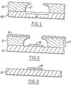
- FIGS 1, 2 and 3 illustrate a process according to the present invention.
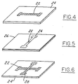
- Figures 4, 5 and 6 illustrate a method for making a structure carrying two metallizations in contact with each other which employs a process according to the present invention.
- a layer of resist material 12 is provided in a desired pattern on a surface of a substrate 10 (shown as a semiconductor material, e.g., silicon).
- the resist 12 defines uncovered surface areas 14 and has undercut side walls 12′ adjacent the uncovered surface areas 14.
- substrate materials to which it would be desirable to apply a patterned layer of metal according to the process of this invention, will be apparent to those skilled in the art in view of the present disclosure.
- Exemplary of such materials which are commercially available are semi-conductor materials, glass, sapphire and polished alumina.
- the substrate material has a high degree of surface polish.
- the substrate also should possess a coefficient of thermal expansion different from that of the resist materials applied thereon.
- the substrate may be of any of various shapes, generally, however for use in microelectronic devices, the substrate would be a wafer, e.g, being a disc having two broad faces and a thin cylindrical edge surface or being a rectangular solid having two broad faces and four thin edge surfaces. Fragments or sections of a wafer could also be used instead of a complete wafer.
- the substrate would be single crystal silicon wafers of (100) or (111) crystal orientation.
- a resist material shown as 12 in Fig. 1, is provided in a desired pattern on a surface of a substrate 10.
- the resist material may be selected from any of the known various types of resist material, including, but not limited to, electron beam resists and photoresists.
- Photoresist materials are commonly used in a wide number of industrial processes where it is desired to provide detailed pattern on a substrate surface in thin films applied thereto or to provide regions of altered character as contrasted to other surface portions of the substrate.
- Such photoresist materials are photo sensitive in nature, being characterized by a differential reactivity to specific liquid solvents after exposure to actinic radiation or other energy source effective for the particular photoresist material used, such as ultraviolet radiation.
- a standard photographic practice in employing photoresist layers as patterns involves the application of a layer of photoresist material to a substrate, followed by the selective exposure of the photoresist layer to an energy source, wherein portions of the photoresist layer are changed in character due to their exposure to the energy source. After such exposure, the photoresist layer is then developed by a "wet development process" employing liquid chemical solvents to selectively remove portions of the photoresist for providing the desired pattern therein. Negative and positive photoresist materials are available for this purpose.
- a negative photoresist material In a negative photoresist material, the portion of a layer thereof exposed to the energy source is changed in its chemical character being polymerized as contrasted to the nonexposed portion and rendering it insoluble with respect to the liquid chemical solvent which removes the nonexposed portion of the negative photoresist layer in producing the desired pattern therein.
- a negative photoresist material is Hunt HNR (trademark, Apache Chemicals, Div., Hunt Chemical Corp., Seward, IL).
- a positive photoresist layer For a positive photoresist layer, the situation is reversed in that the portion thereof exposed to the energy source is rendered soluble to the liquid solvent, while the nonexposed portion is insoluble with respect thereto and remains after development in forming the desired pattern.
- positive photoresist materials are Shipley MP 1470 (trademark, Shipley Co., Inc., Newton, MA), and MacDermid 914 (trademark, Mac Dermid, Inc., Waterbury, CT). Positive photoresist materials are preferred for use in the process of this invention.
- the resist material is processed to a soft cure, i.e., the resist material is cured at a lower temperature so as to leave the resist material at less than maximum hardness. It has been found that photoresist materials which have been soft cured detach more rapidly from the surface of the substrate according to this invention when subjected to sufficiently low temperatures than photoresist materials which have been cured to maximum hardness when subjected to the same temperatures.
- undercut side walls in the resist material can be done by numerous techniques well known to those skilled in the art.
- One way to obtain the undercut structure is to apply a coating of two or more resist layers with widely different solubilities. After, e.g., an electron beam exposure, a developer is chosen that develops the top layer at least 10 times slower than the bottom layer. Alternately, two mutually exclusive developers can be used for the successive development of the two layers. Both of these approaches result in undercut resist profiles suitable for the cryogenic lift-off of metal according to the invention.
- Still another method for forming an undercut resist layer involves using a single layer of uv-exposed resist whose surface has been modified before or after exposure by means of a chlorobenzene soak process.
- the chlorobenzene modifies the resist layer so as to reduce the solubility of the modified layer in the developer solution. In this way undercut side walls are formed in resist.
- This last technique is described in detail in "Single-Step Optical Lift-Off Process" by M. Hatzakis et al, IBM J. Res. Develop., Vol. 24, No. 4, July 1980. Techniques such as those described above as well as others known in the art may be employed to provide a discontinuous layer of resist material having undercut side walls according to the process of the invention.
- the process further comprises applying a layer of metal.
- a first portion 16 of the metal will deposit on the surface of the resist material 12 and a second portion 18 of the metal will deposit on the an uncovered surface area 14 of the substrate 10, forming a layered article 20.
- the metal is selected from any metal which is suitably adherent to the substrate.
- Exemplary of metals which can be used as this layer in the invention include aluminum, iron, nickel, copper, lead, silver, chromium, tungsten, tin, platinum, molybdenum, gold and their alloys. Selection of one of these or still another metal will be within the skill of those in the art in view of the present disclosure. Selection of the optimal metal to be so employed will depend on such considerations as its electrical and thermal conductivity, melting point, and corrosion resistance in view of the intended use of a device made using the invention process.
- the layer of metal is applied so that the first portion of the metal 16 and the second portion of the metal 18 do not contact each other.
- the metal may be applied by any suitable technique including, e.g., sputtering or evaporation techniques, which are well known to those skilled in the art. Exemplary of those techniques are those taught in the texts: Thin Film Processes , edited by John L. Vossen and Werner Kern, Academic Press, N.Y., 1978, and Thin Films Phenomena by K. L. Chopra, McGraw Hill, N Y., 1969.
- the first portion 16 of the metal and the second portion 18 of the metal are applied so that they do not contact one another in order that when the resist layer 12 detaches according to the invention process taking with it the first portion 16 of metal deposited on the resist layer, the second portion 18 of the metal is not affected.
- the thickness of the applied metal layer would be no thicker than that of the resist layer.
- the thickness of a metal layer applied on a semiconductor substrate is generally between about 0.1 and about 2 ⁇ m. While the metal layer applied in the process disclosed herein is not limited to any particular thickness, its thickness is understood to be optimally inherently linked to the resist thickness in the manner described.
- the profile of the second portion 18 of metal as shown in Figure 2 would be that which results when the metal is applied by commonly used techniques such as evaporation or sputtering, preferably the former, from a source above the substrate surface.
- the undercut resist layer 12 would cause application of the second portion 18 of the metal layer in a pattern which does not cover entire uncovered surface areas 14 of the substrate, but rather covers a region of the uncovered surface areas of the substrate surface which are exposed by the undercut edges of the resist layer 12. This causes the second portion 18 of the metal layer to be spaced apart from the undercut sides 12′ of the resist layer in proximity thereto.
- the invention process does not require such a profile for the second portion 12 of the metal layer.
- the second portion of the metal layer may cover all uncovered surface areas of the substrate surface or a part thereof, as described above.
- the second portion may also contact the sides 12′, in part or in total, of the resist layer 12, as long as the second portion 18 of the metal does not contact the first portion 16 of metal.
- the layered article is subjected to a temperature sufficiently low to cause the resist layer 12 to detach, i.e., lift-off, from the surface of substrate 10.
- layered article is meant at least the metal layer, the resist layer and the surface of the substrate.
- the layered article may comprise the metal layer, the resist layer and the entire substrate which could be subjected to the low temperature.
- One way to subject the layered article to a sufficiently low temperature to cause the resist layer to detach from the surface of the substrate is to subject the layered article to a cryogenic temperature, such as by exposure to liquid nitrogen.
- the article could be subjected to a sufficiently low temperature by by use of refrigerants, e.g., freons, or refrigerated solvents, e.g., dry ice/methanol.
- refrigerants e.g., freons
- refrigerated solvents e.g., dry ice/methanol.
- substrate 10 having a pattern of the second portion of metal 18, as shown in Figure 3.
- This example describes a lift-off process according to the invention.
- a 10 cm (four inch) diameter (100) p-type silicon wafer, approximately 620 ⁇ m thick was cleaned in 50% H2O2 - 50% H2SO4 solution.
- the wafer was then spin coated firstly at 5000 rpm with a hexamethyl disilazane (HMDS coupling-agent) and then at 3500 rpm with Shipley 1470 (trademark, Shipley Co., Inc., Newton, MA) resist to produce a photoresist film of 2 ⁇ m thickness.
- the wafer was then soft baked at 70°C for 15 minutes and subsequently soaked in 100% chlorobenzene for 5 minutes.
- the photoresist was then exposed to a pattern using a commercial mask aligner with power of 9.5 mW/cm2 for 9 seconds.
- the pattern was developed in a 1:1 solution of Microposit Developer MF-312 (trademark, Shipley Co., Inc., Newton, MA):water for 2 minutes.
- the wafer was dried and transferred to the planetary stage of an electron beam evaporator equipped with an aluminum target.
- a 1 ⁇ m thick film of aluminum was then deposited onto the wafer/resist assembly. After removal from the vacuum system, the metalized wafer was submerged for approximately 5 seconds in liquid nitrogen. Upon removal, the desired pattern of aluminum was evident on the wafer and the unwanted portions of the aluminum film remained behind in the liquid nitrogen bath adhering to the photoresist which had detached from the surface of the wafer.
- a structure comprising two metallizations on a sapphire substrate is made using (a) a subtractive etching process to provide a patterned aluminum first layer and thereafter (b) the process of this invention to provide a patterned nickel second layer in contact with the first layer.
- an aluminum first layer metallization 22 is deposited by a subtractive etching process on a sapphire substrate 24 which comprises using a positive photoresist, development, and removal of unwanted aluminum by one of the various etchants known to those familiar with the art.
- a second level metallization consisting of nickel is subsequently applied using the process of this invention.
- a resist layer 26 is provided in a pattern on the surface of the substrate which leaves an area of the substrate exposed (in this case the substrate includes portions of the sapphire substrate 24 and portions of the aluminum metallization 22).
- a nickel layer is then deposited on the assembly by an electron-beam evaporative process producing an overall coverage of the assembly.
- the assembly is then subjected to contact with a bath of liquid nitrogen.
- the resist and nickel lying thereon detach from the surface of the substrate according to the process of the invention, leaving behind two metallizations which are in contact as shown in Figure 6.
Landscapes
- Physics & Mathematics (AREA)
- General Physics & Mathematics (AREA)
- Photosensitive Polymer And Photoresist Processing (AREA)
- Manufacturing Of Printed Circuit Boards (AREA)
- Exposure Of Semiconductors, Excluding Electron Or Ion Beam Exposure (AREA)
- Internal Circuitry In Semiconductor Integrated Circuit Devices (AREA)
Abstract
Claims (9)
- Procédé pour le décollage cryogénique d'une matière métal/réserve à enlever d'une surface d'un substrat, ce procédé comprenant :- la fourniture d'une couche de matière de réserve modérément durcie, formant un motif voulu sur une surface d'un substrat, ledit substrat possédant un coefficient de dilatation thermique différent de celui de ladite matière de réserve et ladite couche (i) délimitant des zones de surfaces non recouvertes dudit substrat, et (ii) ayant des parois latérales détalonnées près desdites zones de surfaces non recouvertes;- puis l'application d'une couche de métal de sorte qu'une première partie de ces dépôts de métal sur la surface de ladite matière de réserve et une seconde partie desdits dépôts de métaux sur les zones de surfaces non recouvertes dudit substrat forment un article formé de couches stratifiées, ledit métal adhérant à ladite surface dudit substrat, ladite première partie et ladite seconde partie de métal n'étant pas mutuellement en contact; et- puis la soumission de cet article formé de couches ou stratifié à une température suffisamment basse pour provoquer le détachement de ladite couche de réserve qui se sépare ainsi de ladite surface dudit substrat.
- Procédé selon la revendication 1, dans lequel ladite matière de réserve est choisi parmi des matières de photo-réserve positive et des matières de photo-réserve négative.
- Procédé selon la revendication 1, dans lequel ledit substrat est une matière semi-conductrice.
- Procédé selon la revendication 3, dans lequel ladite matière semi-conductrice est choisi parmi du silicium, de l'arséniure de gallium et du phosphure d'indium.
- Procédé selon la revendication 4, dans lequel ledit substrat est une partie ou "puce" de silicium monocristallin.
- Procédé selon la revendication 1, dans lequel ledit métal est choisi parmi l'aluminium, le fer, le nickel, le cuivre, le plomb, l'argent, le chrome, le tungstène, l'étain, le platine, le molybdène, l'or et des alliages de deux ou plusieurs quelconques d'entre eux.
- Procédé selon la revendication 1, dans lequel une couche de métal est appliquée par une technique choisie parmi les méthodes d'évaporation et de dépôt par une pulvérisation électrique.
- Procédé selon la revendication 1, dans lequel ledit article stratifié est soumis à une température cryogénique pour provoquer le détachement de ladite couche de réserve de ladite surface du dudit substrat.
- Procédé selon la revendication 8, dans lequel ledit article stratifié est soumis à de l'azote liquide pour provoquer le détachement de ladite couche de réserve qui se sépare ainsi de ladite surface dudit substrat.
Applications Claiming Priority (3)
| Application Number | Priority Date | Filing Date | Title |
|---|---|---|---|
| US211648 | 1988-06-27 | ||
| US07/211,648 US4871651A (en) | 1988-06-27 | 1988-06-27 | Cryogenic process for metal lift-off |
| PCT/US1989/002592 WO1990000310A1 (fr) | 1988-06-27 | 1989-06-14 | Procede cryogenique de decollement de metal |
Publications (2)
| Publication Number | Publication Date |
|---|---|
| EP0401314A1 EP0401314A1 (fr) | 1990-12-12 |
| EP0401314B1 true EP0401314B1 (fr) | 1994-08-31 |
Family
ID=22787803
Family Applications (1)
| Application Number | Title | Priority Date | Filing Date |
|---|---|---|---|
| EP89909110A Expired - Lifetime EP0401314B1 (fr) | 1988-06-27 | 1989-06-14 | Procede cryogenique de decollement de metal |
Country Status (7)
| Country | Link |
|---|---|
| US (1) | US4871651A (fr) |
| EP (1) | EP0401314B1 (fr) |
| JP (1) | JPH03500227A (fr) |
| AU (1) | AU4045689A (fr) |
| CA (1) | CA1332323C (fr) |
| DE (1) | DE68917918T2 (fr) |
| WO (1) | WO1990000310A1 (fr) |
Families Citing this family (16)
| Publication number | Priority date | Publication date | Assignee | Title |
|---|---|---|---|---|
| US5234539A (en) * | 1990-02-23 | 1993-08-10 | France Telecom (C.N.E.T.) | Mechanical lift-off process of a metal layer on a polymer |
| FR2658976A1 (fr) * | 1990-02-23 | 1991-08-30 | Schiltz Andre | Procede de lift-off (enlevement d'une couche par decollement d'une couche sous-jacente) mecanique. |
| JP2738623B2 (ja) * | 1992-04-23 | 1998-04-08 | 三菱電機株式会社 | 回折格子の形成方法 |
| US5559057A (en) * | 1994-03-24 | 1996-09-24 | Starfire Electgronic Development & Marketing Ltd. | Method for depositing and patterning thin films formed by fusing nanocrystalline precursors |
| EP0708372B1 (fr) * | 1994-10-21 | 2000-03-22 | Ngk Insulators, Ltd. | Procédé de décollage à une seule couche de photoréserve pour former des motifs sur un support |
| US5931721A (en) * | 1994-11-07 | 1999-08-03 | Sumitomo Heavy Industries, Ltd. | Aerosol surface processing |
| US5967156A (en) * | 1994-11-07 | 1999-10-19 | Krytek Corporation | Processing a surface |
| US6500758B1 (en) * | 2000-09-12 | 2002-12-31 | Eco-Snow Systems, Inc. | Method for selective metal film layer removal using carbon dioxide jet spray |
| TWI220770B (en) * | 2003-06-11 | 2004-09-01 | Ind Tech Res Inst | Method for forming a conductive layer |
| US6919623B2 (en) * | 2003-12-12 | 2005-07-19 | The Boeing Company | Hydrogen diffusion hybrid port and method of forming |
| US20050282307A1 (en) * | 2004-06-21 | 2005-12-22 | Daniels John J | Particulate for organic and inorganic light active devices and methods for fabricating the same |
| JP2006128544A (ja) * | 2004-11-01 | 2006-05-18 | Disco Abrasive Syst Ltd | ウェーハの加工方法 |
| CA2500611A1 (fr) * | 2005-03-04 | 2006-09-04 | Quadra Industrial Services Ontario Inc. | Methode d'enlevement des residus colles de metaux ferreux ou non ferreux dans les poches a laitier |
| US9012133B2 (en) * | 2011-08-30 | 2015-04-21 | International Business Machines Corporation | Removal of alkaline crystal defects in lithographic patterning |
| JP7279024B2 (ja) * | 2017-09-12 | 2023-05-22 | アプライド マテリアルズ インコーポレイテッド | 化学エッチングによる選択的堆積の欠陥除去 |
| US11033930B2 (en) | 2018-01-08 | 2021-06-15 | Applied Materials, Inc. | Methods and apparatus for cryogenic gas stream assisted SAM-based selective deposition |
Family Cites Families (3)
| Publication number | Priority date | Publication date | Assignee | Title |
|---|---|---|---|---|
| US4370288A (en) * | 1980-11-18 | 1983-01-25 | Motorola, Inc. | Process for forming self-supporting semiconductor film |
| US4631250A (en) * | 1985-03-13 | 1986-12-23 | Research Development Corporation Of Japan | Process for removing covering film and apparatus therefor |
| US4662989A (en) * | 1985-10-04 | 1987-05-05 | Honeywell Inc. | High efficiency metal lift-off process |
-
1988
- 1988-06-27 US US07/211,648 patent/US4871651A/en not_active Expired - Fee Related
-
1989
- 1989-05-30 CA CA000601148A patent/CA1332323C/fr not_active Expired - Fee Related
- 1989-06-14 DE DE68917918T patent/DE68917918T2/de not_active Expired - Lifetime
- 1989-06-14 JP JP1508511A patent/JPH03500227A/ja active Pending
- 1989-06-14 AU AU40456/89A patent/AU4045689A/en not_active Abandoned
- 1989-06-14 WO PCT/US1989/002592 patent/WO1990000310A1/fr not_active Ceased
- 1989-06-14 EP EP89909110A patent/EP0401314B1/fr not_active Expired - Lifetime
Also Published As
| Publication number | Publication date |
|---|---|
| WO1990000310A1 (fr) | 1990-01-11 |
| DE68917918T2 (de) | 1995-01-05 |
| JPH03500227A (ja) | 1991-01-17 |
| DE68917918D1 (de) | 1994-10-06 |
| US4871651A (en) | 1989-10-03 |
| CA1332323C (fr) | 1994-10-11 |
| EP0401314A1 (fr) | 1990-12-12 |
| AU4045689A (en) | 1990-01-23 |
Similar Documents
| Publication | Publication Date | Title |
|---|---|---|
| EP0401314B1 (fr) | Procede cryogenique de decollement de metal | |
| US4088490A (en) | Single level masking process with two positive photoresist layers | |
| US4533624A (en) | Method of forming a low temperature multilayer photoresist lift-off pattern | |
| US4218532A (en) | Photolithographic technique for depositing thin films | |
| US4352716A (en) | Dry etching of copper patterns | |
| EP0083397B1 (fr) | Procédé de réalisation de microcircuits électroniques | |
| US4115120A (en) | Method of forming thin film patterns by differential pre-baking of resist | |
| US4132586A (en) | Selective dry etching of substrates | |
| US3639185A (en) | Novel etchant and process for etching thin metal films | |
| US4670097A (en) | Method for patterning transparent layers on a transparent substrate | |
| US3443944A (en) | Method of depositing conductive patterns on a substrate | |
| US4451554A (en) | Method of forming thin-film pattern | |
| US5126007A (en) | Method for etching a pattern in layer of gold | |
| JPS5851412B2 (ja) | 半導体装置の微細加工方法 | |
| US3984300A (en) | Semiconductor pattern delineation by sputter etching process | |
| US3772102A (en) | Method of transferring a desired pattern in silicon to a substrate layer | |
| US3986876A (en) | Method for making a mask having a sloped relief | |
| US3644180A (en) | Methods of using inorganic resists | |
| EP0058214B1 (fr) | Méthode pour augmenter la résistance de la surface d'un matériau solide à la gravure | |
| KR20010113735A (ko) | 1 미크론 이하의 폭을 갖는 금속 라인을 형성하기에적절한 패턴의 제조 방법 | |
| Jelks et al. | A simple method for fabricating lines of 0.15‐μ width using optical lithography | |
| US3773670A (en) | Novel etchant for etching thin metal films | |
| US6686128B1 (en) | Method of fabricating patterned layers of material upon a substrate | |
| US3551176A (en) | Method for providing holes in glass | |
| US5895271A (en) | Metal film forming method |
Legal Events
| Date | Code | Title | Description |
|---|---|---|---|
| PUAI | Public reference made under article 153(3) epc to a published international application that has entered the european phase |
Free format text: ORIGINAL CODE: 0009012 |
|
| 17P | Request for examination filed |
Effective date: 19900102 |
|
| AK | Designated contracting states |
Kind code of ref document: A1 Designated state(s): DE FR GB NL SE |
|
| 17Q | First examination report despatched |
Effective date: 19930210 |
|
| GRAA | (expected) grant |
Free format text: ORIGINAL CODE: 0009210 |
|
| AK | Designated contracting states |
Kind code of ref document: B1 Designated state(s): DE FR GB NL SE |
|
| PG25 | Lapsed in a contracting state [announced via postgrant information from national office to epo] |
Ref country code: FR Effective date: 19940831 |
|
| REF | Corresponds to: |
Ref document number: 68917918 Country of ref document: DE Date of ref document: 19941006 |
|
| PG25 | Lapsed in a contracting state [announced via postgrant information from national office to epo] |
Ref country code: SE Effective date: 19941130 |
|
| EN | Fr: translation not filed | ||
| PG25 | Lapsed in a contracting state [announced via postgrant information from national office to epo] |
Ref country code: GB Effective date: 19950614 |
|
| PLBE | No opposition filed within time limit |
Free format text: ORIGINAL CODE: 0009261 |
|
| STAA | Information on the status of an ep patent application or granted ep patent |
Free format text: STATUS: NO OPPOSITION FILED WITHIN TIME LIMIT |
|
| 26N | No opposition filed | ||
| PG25 | Lapsed in a contracting state [announced via postgrant information from national office to epo] |
Ref country code: NL Effective date: 19960101 |
|
| GBPC | Gb: european patent ceased through non-payment of renewal fee |
Effective date: 19950614 |
|
| NLV4 | Nl: lapsed or anulled due to non-payment of the annual fee |
Effective date: 19960101 |
|
| PGFP | Annual fee paid to national office [announced via postgrant information from national office to epo] |
Ref country code: DE Payment date: 19970701 Year of fee payment: 9 |
|
| PG25 | Lapsed in a contracting state [announced via postgrant information from national office to epo] |
Ref country code: DE Free format text: LAPSE BECAUSE OF THE APPLICANT RENOUNCES Effective date: 19980516 |