EP0708372B1 - Procédé de décollage à une seule couche de photoréserve pour former des motifs sur un support - Google Patents
Procédé de décollage à une seule couche de photoréserve pour former des motifs sur un support Download PDFInfo
- Publication number
- EP0708372B1 EP0708372B1 EP95305923A EP95305923A EP0708372B1 EP 0708372 B1 EP0708372 B1 EP 0708372B1 EP 95305923 A EP95305923 A EP 95305923A EP 95305923 A EP95305923 A EP 95305923A EP 0708372 B1 EP0708372 B1 EP 0708372B1
- Authority
- EP
- European Patent Office
- Prior art keywords
- resist
- substrate
- resist layer
- minutes
- heat treatment
- Prior art date
- Legal status (The legal status is an assumption and is not a legal conclusion. Google has not performed a legal analysis and makes no representation as to the accuracy of the status listed.)
- Expired - Lifetime
Links
- 238000000034 method Methods 0.000 title claims description 83
- 230000008569 process Effects 0.000 title claims description 80
- 239000000758 substrate Substances 0.000 title claims description 57
- 229910052751 metal Inorganic materials 0.000 claims description 46
- 239000002184 metal Substances 0.000 claims description 46
- MVPPADPHJFYWMZ-UHFFFAOYSA-N chlorobenzene Chemical compound ClC1=CC=CC=C1 MVPPADPHJFYWMZ-UHFFFAOYSA-N 0.000 claims description 36
- CSCPPACGZOOCGX-UHFFFAOYSA-N Acetone Chemical compound CC(C)=O CSCPPACGZOOCGX-UHFFFAOYSA-N 0.000 claims description 18
- 239000000463 material Substances 0.000 claims description 17
- 238000010438 heat treatment Methods 0.000 claims description 15
- 238000000151 deposition Methods 0.000 claims description 14
- 239000003849 aromatic solvent Substances 0.000 claims description 13
- 229920002120 photoresistant polymer Polymers 0.000 claims description 13
- 230000008021 deposition Effects 0.000 claims description 12
- 239000002904 solvent Substances 0.000 claims description 9
- 229910052804 chromium Inorganic materials 0.000 claims description 5
- 229910001218 Gallium arsenide Inorganic materials 0.000 claims description 4
- 238000013019 agitation Methods 0.000 claims description 4
- 229910052782 aluminium Inorganic materials 0.000 claims description 4
- 229920005989 resin Polymers 0.000 claims description 4
- 239000011347 resin Substances 0.000 claims description 4
- 229910052737 gold Inorganic materials 0.000 claims description 3
- 229910052759 nickel Inorganic materials 0.000 claims description 3
- 229910052697 platinum Inorganic materials 0.000 claims description 3
- 230000005855 radiation Effects 0.000 claims description 3
- 229910052715 tantalum Inorganic materials 0.000 claims description 3
- 229910052719 titanium Inorganic materials 0.000 claims description 3
- 229910003327 LiNbO3 Inorganic materials 0.000 claims description 2
- 229910045601 alloy Inorganic materials 0.000 claims description 2
- 239000000956 alloy Substances 0.000 claims description 2
- 239000000203 mixture Substances 0.000 claims description 2
- 229920003986 novolac Polymers 0.000 claims description 2
- 239000012780 transparent material Substances 0.000 claims description 2
- 238000001465 metallisation Methods 0.000 description 34
- 238000004519 manufacturing process Methods 0.000 description 7
- 230000000052 comparative effect Effects 0.000 description 5
- 238000012545 processing Methods 0.000 description 5
- 239000000126 substance Substances 0.000 description 5
- VYZAMTAEIAYCRO-UHFFFAOYSA-N Chromium Chemical compound [Cr] VYZAMTAEIAYCRO-UHFFFAOYSA-N 0.000 description 4
- PXHVJJICTQNCMI-UHFFFAOYSA-N Nickel Chemical compound [Ni] PXHVJJICTQNCMI-UHFFFAOYSA-N 0.000 description 4
- 239000011651 chromium Substances 0.000 description 4
- 238000010586 diagram Methods 0.000 description 4
- 150000002739 metals Chemical class 0.000 description 4
- BASFCYQUMIYNBI-UHFFFAOYSA-N platinum Chemical compound [Pt] BASFCYQUMIYNBI-UHFFFAOYSA-N 0.000 description 4
- XAGFODPZIPBFFR-UHFFFAOYSA-N aluminium Chemical compound [Al] XAGFODPZIPBFFR-UHFFFAOYSA-N 0.000 description 3
- 238000011161 development Methods 0.000 description 3
- 230000003287 optical effect Effects 0.000 description 3
- 239000004215 Carbon black (E152) Substances 0.000 description 2
- RTAQQCXQSZGOHL-UHFFFAOYSA-N Titanium Chemical compound [Ti] RTAQQCXQSZGOHL-UHFFFAOYSA-N 0.000 description 2
- 238000010521 absorption reaction Methods 0.000 description 2
- 238000004873 anchoring Methods 0.000 description 2
- 238000004140 cleaning Methods 0.000 description 2
- 230000000694 effects Effects 0.000 description 2
- 238000005530 etching Methods 0.000 description 2
- 230000008020 evaporation Effects 0.000 description 2
- 238000001704 evaporation Methods 0.000 description 2
- PCHJSUWPFVWCPO-UHFFFAOYSA-N gold Chemical compound [Au] PCHJSUWPFVWCPO-UHFFFAOYSA-N 0.000 description 2
- 239000010931 gold Substances 0.000 description 2
- 229930195733 hydrocarbon Natural products 0.000 description 2
- 150000002430 hydrocarbons Chemical class 0.000 description 2
- 230000004048 modification Effects 0.000 description 2
- 238000012986 modification Methods 0.000 description 2
- 238000004886 process control Methods 0.000 description 2
- 238000002791 soaking Methods 0.000 description 2
- GUVRBAGPIYLISA-UHFFFAOYSA-N tantalum atom Chemical compound [Ta] GUVRBAGPIYLISA-UHFFFAOYSA-N 0.000 description 2
- 239000010936 titanium Substances 0.000 description 2
- 239000000654 additive Substances 0.000 description 1
- 230000000996 additive effect Effects 0.000 description 1
- 238000000637 aluminium metallisation Methods 0.000 description 1
- 238000013459 approach Methods 0.000 description 1
- 230000004888 barrier function Effects 0.000 description 1
- 230000005540 biological transmission Effects 0.000 description 1
- 230000015572 biosynthetic process Effects 0.000 description 1
- 230000008859 change Effects 0.000 description 1
- 238000003486 chemical etching Methods 0.000 description 1
- 238000005229 chemical vapour deposition Methods 0.000 description 1
- 239000011248 coating agent Substances 0.000 description 1
- 238000000576 coating method Methods 0.000 description 1
- 238000006482 condensation reaction Methods 0.000 description 1
- 230000001419 dependent effect Effects 0.000 description 1
- 238000009792 diffusion process Methods 0.000 description 1
- 239000006185 dispersion Substances 0.000 description 1
- 238000004090 dissolution Methods 0.000 description 1
- 238000010894 electron beam technology Methods 0.000 description 1
- 238000005516 engineering process Methods 0.000 description 1
- 230000008570 general process Effects 0.000 description 1
- 239000011521 glass Substances 0.000 description 1
- 239000012535 impurity Substances 0.000 description 1
- 230000006698 induction Effects 0.000 description 1
- 238000003754 machining Methods 0.000 description 1
- 230000007246 mechanism Effects 0.000 description 1
- 239000002905 metal composite material Substances 0.000 description 1
- 230000035515 penetration Effects 0.000 description 1
- 238000000206 photolithography Methods 0.000 description 1
- 238000001020 plasma etching Methods 0.000 description 1
- 238000003908 quality control method Methods 0.000 description 1
- 239000013557 residual solvent Substances 0.000 description 1
- 238000004544 sputter deposition Methods 0.000 description 1
- XLYOFNOQVPJJNP-UHFFFAOYSA-N water Substances O XLYOFNOQVPJJNP-UHFFFAOYSA-N 0.000 description 1
- 238000003079 width control Methods 0.000 description 1
Images


Classifications
-
- G—PHYSICS
- G03—PHOTOGRAPHY; CINEMATOGRAPHY; ANALOGOUS TECHNIQUES USING WAVES OTHER THAN OPTICAL WAVES; ELECTROGRAPHY; HOLOGRAPHY
- G03F—PHOTOMECHANICAL PRODUCTION OF TEXTURED OR PATTERNED SURFACES, e.g. FOR PRINTING, FOR PROCESSING OF SEMICONDUCTOR DEVICES; MATERIALS THEREFOR; ORIGINALS THEREFOR; APPARATUS SPECIALLY ADAPTED THEREFOR
- G03F7/00—Photomechanical, e.g. photolithographic, production of textured or patterned surfaces, e.g. printing surfaces; Materials therefor, e.g. comprising photoresists; Apparatus specially adapted therefor
- G03F7/16—Coating processes; Apparatus therefor
- G03F7/168—Finishing the coated layer, e.g. drying, baking, soaking
-
- G—PHYSICS
- G03—PHOTOGRAPHY; CINEMATOGRAPHY; ANALOGOUS TECHNIQUES USING WAVES OTHER THAN OPTICAL WAVES; ELECTROGRAPHY; HOLOGRAPHY
- G03F—PHOTOMECHANICAL PRODUCTION OF TEXTURED OR PATTERNED SURFACES, e.g. FOR PRINTING, FOR PROCESSING OF SEMICONDUCTOR DEVICES; MATERIALS THEREFOR; ORIGINALS THEREFOR; APPARATUS SPECIALLY ADAPTED THEREFOR
- G03F7/00—Photomechanical, e.g. photolithographic, production of textured or patterned surfaces, e.g. printing surfaces; Materials therefor, e.g. comprising photoresists; Apparatus specially adapted therefor
- G03F7/26—Processing photosensitive materials; Apparatus therefor
- G03F7/40—Treatment after imagewise removal, e.g. baking
-
- G—PHYSICS
- G03—PHOTOGRAPHY; CINEMATOGRAPHY; ANALOGOUS TECHNIQUES USING WAVES OTHER THAN OPTICAL WAVES; ELECTROGRAPHY; HOLOGRAPHY
- G03F—PHOTOMECHANICAL PRODUCTION OF TEXTURED OR PATTERNED SURFACES, e.g. FOR PRINTING, FOR PROCESSING OF SEMICONDUCTOR DEVICES; MATERIALS THEREFOR; ORIGINALS THEREFOR; APPARATUS SPECIALLY ADAPTED THEREFOR
- G03F7/00—Photomechanical, e.g. photolithographic, production of textured or patterned surfaces, e.g. printing surfaces; Materials therefor, e.g. comprising photoresists; Apparatus specially adapted therefor
- G03F7/26—Processing photosensitive materials; Apparatus therefor
- G03F7/42—Stripping or agents therefor
- G03F7/422—Stripping or agents therefor using liquids only
-
- H—ELECTRICITY
- H05—ELECTRIC TECHNIQUES NOT OTHERWISE PROVIDED FOR
- H05K—PRINTED CIRCUITS; CASINGS OR CONSTRUCTIONAL DETAILS OF ELECTRIC APPARATUS; MANUFACTURE OF ASSEMBLAGES OF ELECTRICAL COMPONENTS
- H05K3/00—Apparatus or processes for manufacturing printed circuits
- H05K3/10—Apparatus or processes for manufacturing printed circuits in which conductive material is applied to the insulating support in such a manner as to form the desired conductive pattern
- H05K3/14—Apparatus or processes for manufacturing printed circuits in which conductive material is applied to the insulating support in such a manner as to form the desired conductive pattern using spraying techniques to apply the conductive material, e.g. vapour evaporation
- H05K3/143—Masks therefor
Definitions
- the resist is then developed by immersion in a standard developing chemical (e.g., Shiply Miroposit 303A) for about 15 seconds, to form a patterned resist having a latent image of the desired pattern to be formed on the substrate.
- a standard developing chemical e.g., Shiply Miroposit 303A
Landscapes
- Physics & Mathematics (AREA)
- General Physics & Mathematics (AREA)
- Photosensitive Polymer And Photoresist Processing (AREA)
- Weting (AREA)
- Manufacturing Of Printed Circuit Boards (AREA)
- Exposure Of Semiconductors, Excluding Electron Or Ion Beam Exposure (AREA)
Claims (25)
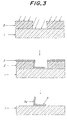
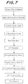
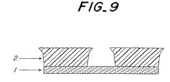
- Procédé de formation d'un motif d'un matériau sur un substrat, comprenant les étapes de :déposer une seule couche de photoréserve (2) sur une surface supérieure dudit substrat (1) pour former une préforme réserve/substrat;soumettre ladite préforme réserve/substrat à un premier traitement thermique pour faire adhérer ladite couche de réserve audit substrat ;immerger ladite préforme réserve/substrat dans un bain d'un solvant aromatique ;soumettre ladite préforme réserve/substrat à un second traitement thermique ;exposer des portions de ladite couche de réserve (2) dans la forme dudit motif ;développer ladite couche de réserve (2) pour élimer ses portions exposées et former une couche de réserve à motif où des ouvertures sont prévues à travers ladite couche de réserve pour exposer la surface supérieure dudit substrat et les parois latérales des ouvertures ont une forme négative ;appliquer une couche (3) d'un matériau de dépôt sur la couche de réserve à motif (2) et à travers ses ouvertures pour former ledit motif dudit matériau de dépôt sur la surface supérieur dudit substrat sans dépôt du matériau sur les parois latérales des ouvertures ;soumettre ledit substrat avec la couche de réserve à motif (2) et le matériau de dépôt (3) qui y est, à un troisième traitement thermique à une température dans la gamme de 100 à 140°C ; etimmerger ledit substrat (1) avec la couche de réserve restante (2) et le matériau de dépôt (3) qui s'y trouve dans un bain de solvant pour élever ladite couche de réserve, avec le matériau qui s'y trouve, tout en laissant ledit motif du matériau de dépôt (3) sur la surface supérieure dudit substrat.
- Procédé de la revendication 1, où ledit troisième traitement thermique est accompli pendant 15-35 minutes.
- Procédé de la revendication 2, où ledit troisième traitement thermique est accompli à une température de 110-130°C pendant 20-30 minutes.
- Procédé de la revendication 3, où ledit troisième traitement thermique est accompli aux environs de 120°C pendant environ 25 minutes.
- Procédé selon l'une quelconque des revendications précédentes, où ladite couche de réserve comprend des résines novolaque.
- Procédé selon l'une quelconque des revendications précédentes, où ledit premier traitement thermique est accompli à une température de 80-100°C.
- Procédé de la revendication 6, où ledit premier traitement thermique est accompli pendant 10-30 minutes.
- Procédé de la revendication 7, où ledit premier traitement thermique est accompli aux environs de 90°C pendant environ 20 minutes.
- Procédé selon l'une quelconque des revendications précédentes, où ledit solvant aromatique comprend du chlorobenzène.
- Procédé de la revendication 9, où ladite préforme de réserve/substrat (1,2) est immergée dans le chlorobenzène pendant 5-25 minutes.
- Procédé de la revendication 10, où ladite préforme réserve/substrat (1,2) est immergée dans le chlorobenzène pendant 10-20 minutes.
- Procédé de la revendication 11, où ladite préforme réserve/substrat (1, 2) est immergée dans le chlorobenzène pendant environ 15 minutes.
- Procédé selon l'une quelconque des revendications précédentes, où ledit deuxième traitement thermique est accompli à une température de 80-100°C.
- Procédé de la revendication 13, où ledit deuxième traitement thermique est accompli pendant 5-15 minutes.
- Procédé de la revendication 14, où ledit deuxième traitement thermique est accompli aux environs de 90°C pendant environ 10 minutes.
- Procédé selon l'une quelconque des revendications précédentes, où un rayonnement UV est utilisé pour exposer des portions de ladite couche de réserve (2).
- Procédé de la revendication 16, où lesdites portions de ladite couche de réserve (2) sont exposées pendant 5-15 secondes.
- Procédé de la revendication 17, où lesdites portions de ladite couche de réserve (2) sont exposées pendant environ 7,5 secondes.
- Procédé selon l'une quelconque des revendications précédentes, où ledit matériau de dépôt (3) comprend du métal.
- Procédé de la revendication 19, où ledit métal est sélectionné parmi Al, Au, Cr, Ni, Pt, Ta, Ti, leurs mélanges et leurs alliages.
- Procédé selon l'une quelconque des revendications précédentes, où ledit substrat (1) comprend un matériau transparent.
- Procédé selon l'une quelconque des revendications précédentes, où ledit substrat (1) comprend l'un de GaAs et LiNbO3.
- Procédé selon l'une quelconque des revendications précédentes, où ledit bain de solvant comprend de l'acétone.
- Procédé selon l'une quelconque des revendications précédentes, où ledit bain de solvant est soumis à une agitation ultrasonore.
- Procédé selon l'une quelconque des revendications précédentes, où ladite couche de réserve avec ledit matériau de dépôt formé dessus est retirée dudit substrat en pas plus de 15 minutes.
Applications Claiming Priority (2)
| Application Number | Priority Date | Filing Date | Title |
|---|---|---|---|
| US325164 | 1989-03-17 | ||
| US32516494A | 1994-10-21 | 1994-10-21 |
Publications (2)
| Publication Number | Publication Date |
|---|---|
| EP0708372A1 EP0708372A1 (fr) | 1996-04-24 |
| EP0708372B1 true EP0708372B1 (fr) | 2000-03-22 |
Family
ID=23266714
Family Applications (1)
| Application Number | Title | Priority Date | Filing Date |
|---|---|---|---|
| EP95305923A Expired - Lifetime EP0708372B1 (fr) | 1994-10-21 | 1995-08-24 | Procédé de décollage à une seule couche de photoréserve pour former des motifs sur un support |
Country Status (4)
| Country | Link |
|---|---|
| US (1) | US5654128A (fr) |
| EP (1) | EP0708372B1 (fr) |
| JP (1) | JPH08124848A (fr) |
| DE (1) | DE69515788T2 (fr) |
Cited By (1)
| Publication number | Priority date | Publication date | Assignee | Title |
|---|---|---|---|---|
| EP4350444A1 (fr) * | 2022-10-07 | 2024-04-10 | Richemont International S.A. | Moule pour la formation de pièces métalliques par croissance métallique et procédé de fabrication d'un tel moule |
Families Citing this family (24)
| Publication number | Priority date | Publication date | Assignee | Title |
|---|---|---|---|---|
| US5334542A (en) * | 1991-11-27 | 1994-08-02 | Oki Electric Industry Co., Ltd. | Method of forming T-shaped electrode |
| DE19646970A1 (de) * | 1996-11-14 | 1998-05-20 | Iris Bohnet | Verfahren zur Bildung einer elektrischen Verbindung bei Multi-Layer-Leiterplatten und Verfahren zur Herstellung einer solchen |
| JP2003533707A (ja) | 1997-08-14 | 2003-11-11 | コダック ポリクロム グラフィックス カンパニーリミテッド | マスク及び電子パーツの製造方法 |
| GB9722861D0 (en) | 1997-10-29 | 1997-12-24 | Horsell Graphic Ind Ltd | Improvements in relation to the manufacture of lithographic printing forms |
| US6469877B1 (en) | 1999-06-15 | 2002-10-22 | Read-Rite Corporation | Spin valve device with improved exchange layer defined track width and method of fabrication |
| US6303416B1 (en) * | 1999-10-07 | 2001-10-16 | International Business Machines Corporation | Method to reduce plasma etch fluting |
| KR100309474B1 (ko) * | 1999-11-05 | 2001-11-02 | 박종섭 | 금속배선 형성방법 |
| US6713237B2 (en) | 2000-07-27 | 2004-03-30 | Seagate Technology Llc | Single layer lift-off method for making an electronic device |
| US20030129843A1 (en) * | 2001-10-05 | 2003-07-10 | Yongming Cai | Planarizing recess etch |
| US6852464B2 (en) | 2002-01-10 | 2005-02-08 | Kodak Polychrome Graphics, Llc | Method of manufacturing a thermally imageable element |
| US6793778B2 (en) | 2002-07-15 | 2004-09-21 | Hitachi Global Storage Technologies Netherlands N.V. | Method of fabricating slider pads for a transducer operating with moving magnetic media |
| US6849372B2 (en) | 2002-07-30 | 2005-02-01 | Kodak Polychrome Graphics | Method of manufacturing imaging compositions |
| JP4085384B2 (ja) * | 2003-06-09 | 2008-05-14 | ミネベア株式会社 | 薄膜パターンの形成方法 |
| KR101112538B1 (ko) * | 2004-07-27 | 2012-03-13 | 삼성전자주식회사 | 박막 트랜지스터 표시판 및 그 제조 방법 |
| US8623737B2 (en) * | 2006-03-31 | 2014-01-07 | Intel Corporation | Sol-gel and mask patterning for thin-film capacitor fabrication, thin-film capacitors fabricated thereby, and systems containing same |
| US20070134943A2 (en) * | 2006-04-02 | 2007-06-14 | Dunnrowicz Clarence J | Subtractive - Additive Edge Defined Lithography |
| US9196270B1 (en) | 2006-12-07 | 2015-11-24 | Western Digital (Fremont), Llc | Method for providing a magnetoresistive element having small critical dimensions |
| KR101446910B1 (ko) * | 2007-12-27 | 2014-10-06 | 주식회사 동진쎄미켐 | 도전성 유리의 투명전도 산화막 패턴 형성방법 및 이에의하여 제조되는 도전성 유리 |
| US8163185B1 (en) | 2008-03-31 | 2012-04-24 | Western Digital (Fremont), Llc | Method and apparatus for lifting off photoresist beneath an overlayer |
| US8316527B2 (en) | 2008-04-01 | 2012-11-27 | Western Digital (Fremont), Llc | Method for providing at least one magnetoresistive device |
| US8349195B1 (en) | 2008-06-27 | 2013-01-08 | Western Digital (Fremont), Llc | Method and system for providing a magnetoresistive structure using undercut free mask |
| TWI417318B (zh) | 2011-07-28 | 2013-12-01 | Ind Tech Res Inst | 聚亞醯胺共聚物及圖案化金屬氧化物層之製造方法 |
| EP2835687B1 (fr) | 2013-08-06 | 2017-03-15 | Ams Ag | Procédé de production d'une structure résistante avec paroi latérale dégagée |
| US12124166B2 (en) | 2017-04-25 | 2024-10-22 | Merck Patent Gmbh | Negative resist formulation for producing undercut pattern profiles |
Family Cites Families (4)
| Publication number | Priority date | Publication date | Assignee | Title |
|---|---|---|---|---|
| US4119483A (en) * | 1974-07-30 | 1978-10-10 | U.S. Philips Corporation | Method of structuring thin layers |
| US4212935A (en) * | 1978-02-24 | 1980-07-15 | International Business Machines Corporation | Method of modifying the development profile of photoresists |
| US4814258A (en) * | 1987-07-24 | 1989-03-21 | Motorola Inc. | PMGI bi-layer lift-off process |
| US4871651A (en) * | 1988-06-27 | 1989-10-03 | Ford Motor Copmpany | Cryogenic process for metal lift-off |
-
1995
- 1995-08-24 EP EP95305923A patent/EP0708372B1/fr not_active Expired - Lifetime
- 1995-08-24 DE DE69515788T patent/DE69515788T2/de not_active Expired - Fee Related
- 1995-09-05 JP JP7250051A patent/JPH08124848A/ja active Pending
-
1996
- 1996-02-15 US US08/601,826 patent/US5654128A/en not_active Expired - Fee Related
Cited By (2)
| Publication number | Priority date | Publication date | Assignee | Title |
|---|---|---|---|---|
| EP4350444A1 (fr) * | 2022-10-07 | 2024-04-10 | Richemont International S.A. | Moule pour la formation de pièces métalliques par croissance métallique et procédé de fabrication d'un tel moule |
| EP4350443A1 (fr) * | 2022-10-07 | 2024-04-10 | Richemont International S.A. | Moule pour la formation de pièces métalliques par croissance métallique et procédé de fabrication d'un tel moule |
Also Published As
| Publication number | Publication date |
|---|---|
| JPH08124848A (ja) | 1996-05-17 |
| US5654128A (en) | 1997-08-05 |
| DE69515788T2 (de) | 2000-09-07 |
| EP0708372A1 (fr) | 1996-04-24 |
| DE69515788D1 (de) | 2000-04-27 |
Similar Documents
| Publication | Publication Date | Title |
|---|---|---|
| EP0708372B1 (fr) | Procédé de décollage à une seule couche de photoréserve pour former des motifs sur un support | |
| CA2011927C (fr) | Methode microlithographique de fabrication de masques de resine photosensible epais a parois verticales | |
| US4533624A (en) | Method of forming a low temperature multilayer photoresist lift-off pattern | |
| US4004044A (en) | Method for forming patterned films utilizing a transparent lift-off mask | |
| US4275286A (en) | Process and mask for ion beam etching of fine patterns | |
| US4202914A (en) | Method of depositing thin films of small dimensions utilizing silicon nitride lift-off mask | |
| US5277749A (en) | Methods and apparatus for relieving stress and resisting stencil delamination when performing lift-off processes that utilize high stress metals and/or multiple evaporation steps | |
| US5360698A (en) | Deep UV lift-off resist process | |
| US3982943A (en) | Lift-off method of fabricating thin films and a structure utilizable as a lift-off mask | |
| US6326231B1 (en) | Use of silicon oxynitride ARC for metal layers | |
| JPS5812344B2 (ja) | 銅を基材とする金属パタ−ンの形成方法 | |
| JPH01137635A (ja) | 反応性イオン・エツチングによって基板材料にパターンを転写する方法 | |
| EP1054296A3 (fr) | Méthode pour réaliser des motifs fins | |
| US4606931A (en) | Lift-off masking method | |
| US6372414B1 (en) | Lift-off process for patterning fine metal lines | |
| EP0030604A2 (fr) | Procédé pour durcir des images photorésistantes | |
| EP0058214B1 (fr) | Méthode pour augmenter la résistance de la surface d'un matériau solide à la gravure | |
| EP0198280A2 (fr) | Procédé pour le développement à sec de profilés métalliques par arrachement | |
| US6686128B1 (en) | Method of fabricating patterned layers of material upon a substrate | |
| JPS5857908B2 (ja) | 薄膜構造体の形成方法 | |
| KR100479960B1 (ko) | 감광막 패턴의 미세 선폭 구현을 위한 난반사 방지막 제조방법 | |
| KR100532737B1 (ko) | 반도체 제조 공정에서의 반사방지막 형성 방법 | |
| KR0144420B1 (ko) | 리소그라피 공정방법 | |
| KR0177869B1 (ko) | 고해상도 포토리소그래피 방법 및 구조 | |
| KR100663015B1 (ko) | 금속배선 및 그 형성 방법 |
Legal Events
| Date | Code | Title | Description |
|---|---|---|---|
| PUAI | Public reference made under article 153(3) epc to a published international application that has entered the european phase |
Free format text: ORIGINAL CODE: 0009012 |
|
| AK | Designated contracting states |
Kind code of ref document: A1 Designated state(s): DE FR GB |
|
| 17P | Request for examination filed |
Effective date: 19961016 |
|
| 17Q | First examination report despatched |
Effective date: 19961129 |
|
| GRAG | Despatch of communication of intention to grant |
Free format text: ORIGINAL CODE: EPIDOS AGRA |
|
| GRAG | Despatch of communication of intention to grant |
Free format text: ORIGINAL CODE: EPIDOS AGRA |
|
| GRAH | Despatch of communication of intention to grant a patent |
Free format text: ORIGINAL CODE: EPIDOS IGRA |
|
| GRAH | Despatch of communication of intention to grant a patent |
Free format text: ORIGINAL CODE: EPIDOS IGRA |
|
| GRAA | (expected) grant |
Free format text: ORIGINAL CODE: 0009210 |
|
| AK | Designated contracting states |
Kind code of ref document: B1 Designated state(s): DE FR GB |
|
| REF | Corresponds to: |
Ref document number: 69515788 Country of ref document: DE Date of ref document: 20000427 |
|
| ET | Fr: translation filed | ||
| PLBE | No opposition filed within time limit |
Free format text: ORIGINAL CODE: 0009261 |
|
| STAA | Information on the status of an ep patent application or granted ep patent |
Free format text: STATUS: NO OPPOSITION FILED WITHIN TIME LIMIT |
|
| 26N | No opposition filed | ||
| REG | Reference to a national code |
Ref country code: GB Ref legal event code: IF02 |
|
| PGFP | Annual fee paid to national office [announced via postgrant information from national office to epo] |
Ref country code: GB Payment date: 20020814 Year of fee payment: 8 |
|
| PGFP | Annual fee paid to national office [announced via postgrant information from national office to epo] |
Ref country code: FR Payment date: 20020821 Year of fee payment: 8 |
|
| PGFP | Annual fee paid to national office [announced via postgrant information from national office to epo] |
Ref country code: DE Payment date: 20020824 Year of fee payment: 8 |
|
| PG25 | Lapsed in a contracting state [announced via postgrant information from national office to epo] |
Ref country code: GB Free format text: LAPSE BECAUSE OF NON-PAYMENT OF DUE FEES Effective date: 20030824 |
|
| PG25 | Lapsed in a contracting state [announced via postgrant information from national office to epo] |
Ref country code: DE Free format text: LAPSE BECAUSE OF NON-PAYMENT OF DUE FEES Effective date: 20040302 |
|
| GBPC | Gb: european patent ceased through non-payment of renewal fee | ||
| PG25 | Lapsed in a contracting state [announced via postgrant information from national office to epo] |
Ref country code: FR Free format text: LAPSE BECAUSE OF NON-PAYMENT OF DUE FEES Effective date: 20040430 |
|
| REG | Reference to a national code |
Ref country code: FR Ref legal event code: ST |