EP0401577B1 - Dispositif semi-conducteur métal-oxyde et sa méthode de fabrication - Google Patents
Dispositif semi-conducteur métal-oxyde et sa méthode de fabrication Download PDFInfo
- Publication number
- EP0401577B1 EP0401577B1 EP90109511A EP90109511A EP0401577B1 EP 0401577 B1 EP0401577 B1 EP 0401577B1 EP 90109511 A EP90109511 A EP 90109511A EP 90109511 A EP90109511 A EP 90109511A EP 0401577 B1 EP0401577 B1 EP 0401577B1
- Authority
- EP
- European Patent Office
- Prior art keywords
- layer
- single crystal
- insulator
- region
- opening
- Prior art date
- Legal status (The legal status is an assumption and is not a legal conclusion. Google has not performed a legal analysis and makes no representation as to the accuracy of the status listed.)
- Expired - Lifetime
Links
Images


Classifications
-
- H—ELECTRICITY
- H10—SEMICONDUCTOR DEVICES; ELECTRIC SOLID-STATE DEVICES NOT OTHERWISE PROVIDED FOR
- H10D—INORGANIC ELECTRIC SEMICONDUCTOR DEVICES
- H10D30/00—Field-effect transistors [FET]
- H10D30/60—Insulated-gate field-effect transistors [IGFET]
- H10D30/67—Thin-film transistors [TFT]
- H10D30/674—Thin-film transistors [TFT] characterised by the active materials
- H10D30/6741—Group IV materials, e.g. germanium or silicon carbide
- H10D30/6743—Silicon
- H10D30/6744—Monocrystalline silicon
-
- H—ELECTRICITY
- H10—SEMICONDUCTOR DEVICES; ELECTRIC SOLID-STATE DEVICES NOT OTHERWISE PROVIDED FOR
- H10D—INORGANIC ELECTRIC SEMICONDUCTOR DEVICES
- H10D30/00—Field-effect transistors [FET]
- H10D30/01—Manufacture or treatment
- H10D30/021—Manufacture or treatment of FETs having insulated gates [IGFET]
- H10D30/031—Manufacture or treatment of FETs having insulated gates [IGFET] of thin-film transistors [TFT]
- H10D30/0321—Manufacture or treatment of FETs having insulated gates [IGFET] of thin-film transistors [TFT] comprising silicon, e.g. amorphous silicon or polysilicon
- H10D30/0323—Manufacture or treatment of FETs having insulated gates [IGFET] of thin-film transistors [TFT] comprising silicon, e.g. amorphous silicon or polysilicon comprising monocrystalline silicon
-
- H—ELECTRICITY
- H10—SEMICONDUCTOR DEVICES; ELECTRIC SOLID-STATE DEVICES NOT OTHERWISE PROVIDED FOR
- H10D—INORGANIC ELECTRIC SEMICONDUCTOR DEVICES
- H10D30/00—Field-effect transistors [FET]
- H10D30/60—Insulated-gate field-effect transistors [IGFET]
- H10D30/67—Thin-film transistors [TFT]
- H10D30/6704—Thin-film transistors [TFT] having supplementary regions or layers in the thin films or in the insulated bulk substrates for controlling properties of the device
- H10D30/6706—Thin-film transistors [TFT] having supplementary regions or layers in the thin films or in the insulated bulk substrates for controlling properties of the device for preventing leakage current
-
- H—ELECTRICITY
- H10—SEMICONDUCTOR DEVICES; ELECTRIC SOLID-STATE DEVICES NOT OTHERWISE PROVIDED FOR
- H10D—INORGANIC ELECTRIC SEMICONDUCTOR DEVICES
- H10D30/00—Field-effect transistors [FET]
- H10D30/60—Insulated-gate field-effect transistors [IGFET]
- H10D30/67—Thin-film transistors [TFT]
- H10D30/6704—Thin-film transistors [TFT] having supplementary regions or layers in the thin films or in the insulated bulk substrates for controlling properties of the device
- H10D30/6713—Thin-film transistors [TFT] having supplementary regions or layers in the thin films or in the insulated bulk substrates for controlling properties of the device characterised by the properties of the source or drain regions, e.g. compositions or sectional shapes
-
- H—ELECTRICITY
- H10—SEMICONDUCTOR DEVICES; ELECTRIC SOLID-STATE DEVICES NOT OTHERWISE PROVIDED FOR
- H10D—INORGANIC ELECTRIC SEMICONDUCTOR DEVICES
- H10D30/00—Field-effect transistors [FET]
- H10D30/60—Insulated-gate field-effect transistors [IGFET]
- H10D30/67—Thin-film transistors [TFT]
- H10D30/674—Thin-film transistors [TFT] characterised by the active materials
- H10D30/6755—Oxide semiconductors, e.g. zinc oxide, copper aluminium oxide or cadmium stannate
-
- H—ELECTRICITY
- H10—SEMICONDUCTOR DEVICES; ELECTRIC SOLID-STATE DEVICES NOT OTHERWISE PROVIDED FOR
- H10D—INORGANIC ELECTRIC SEMICONDUCTOR DEVICES
- H10D30/00—Field-effect transistors [FET]
- H10D30/60—Insulated-gate field-effect transistors [IGFET]
- H10D30/67—Thin-film transistors [TFT]
- H10D30/6757—Thin-film transistors [TFT] characterised by the structure of the channel, e.g. transverse or longitudinal shape or doping profile
Definitions
- the present invention generally relates to a method for fabricating metal-oxide-semiconductor (MOS) devices and more particularly MOS devices having the semoconductor-on-insulator (SOI) structure wherein the back channel effect is eliminated.
- MOS metal-oxide-semiconductor
- SOI semoconductor-on-insulator
- the present invention generally relates to metal-oxide-semiconductor (MOS) devices and more particularly to a MOS device having the semiconductor-on-insulator (SOI) structure wherein the back channel effect is eliminated.
- MOS metal-oxide-semiconductor
- SOI semiconductor-on-insulator
- the increase of operational speed of the device is limited because of the parasitic capacitance formed between the source/drain region and the substrate.
- a MOS transistor having the SOI structure wherein a thin semiconductor layer acting as the substrate is provided on an insulator layer such a parasitic capacitance is decreased significantly and a high speed operation can be achieved.
- Such a device also has a preferable feature of near-ideal isolation between the semiconductor devices and associated therewith, the device generally has a high breakdown voltage.
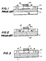
- FIG.1 shows a typical structure of the MOS transistor formed on an SOI substrate.
- the SOI substrate includes a silicon wafer 40 and a silicon oxide layer 41 provided thereon.
- a usual MOS transistor having a single crystal silicon substrate layer 42, source and drain regions 46 formed in the layer 42, a channel region 44 intervening between the source and drain regions 46, and a gate electrode 45 provided on the layer 42.
- the substrate layer 42 is isolated from the substrate layer of adjacent transistors by an isolation region 43 of silicon oxide.
- illustration of the gate insulation film is omitted.
- the back channel is an conductive inversion layer formed by the electric charges in the insulator layer 41, and the formation of the back channel can be reduced when the impurity concentration is increased.
- the back channel effect can be suppressed by increasing the impurity concentration of the semiconductor layer 42 acting as the substrate of the MOS transistor.
- Japanese Laid-open Patent Application No.58-64064 discloses a MOS transistor having the SOI structure wherein the semiconductor layer providing the channel region between the source and the drain regions is doped by ion implantation of impurities such that the concentration level of the impurities therein changes with three distinct concentration levels with the depth of the semiconductor layer. In this prior art, the concentration level adjacent to the insulator layer is maximized for eliminating the back channel effect.
- Fig. 2 shows the general feature of another known technique for eliminating the back channel effect in an MOS transistor.
- the channel region 44 is divided into the normal channel region 44a having a normal impurity concentration level and a back channel effect eliminating region 47 doped to an increased impurity concentration level.
- This region 47 is formed adjacent to the silicon oxide layer 41.
- the region 46 represents the source and drain regions and the region 45 represents the gate electrode.
- the back channel effect is successfully eliminated as a result of the provision of the region 47.
- a structure has a problem of poor breakdown characteristic because of the reason that the region 47 which is doped for example to the p-type with the high concentration level is located in contact with the source or drain region 46 which is doped to the n-type with the high concentration level. More specifically, such a device shows a decrease of the breakdown voltage to less than 10 volts when the region 47 is doped to the level of 2 X 10 17 cm -3 .
- the breakdown voltage is usually about 50 volts.
- the MOS integrated circuits are required to have a breakdown voltage which is about two times as large as the supply voltage in consideration of the noise in the supply voltage and the substrate biasing.
- the breakdown voltage is usually set to 5 volts, the breakdown voltage of 10 volts or less is apparently insufficient.
- MOS transistor disclosed in the Japanese Laid-open Patent Application No.62-104172 having an offset gate structure.
- the MOS transistor is constructed on a silicon single crystal layer provided on a silicon oxide substrate and has an isolated doped region having an increased impurity concentration level in the channel region formed in the silicon single crystal layer in correspondence to a boundary between the silicon oxide substrate and the silicon single crystal layer for eliminating the back channel effect.
- This isolated doped region is provided under an overhanging drain region characterizing the offset gate structure but is separated therefrom and further in an offset relationship with respect to the gate electrode provided on the silicon single crystal layer.
- this prior art MOS transistor can eliminate the back channel effect by the isolated doped region interrupting the formation of the inversion layer extending between the source and drain regions along the boundary to the underlying silicon oxide substrate, it has a problem in that a neutral region is formed in the channel region because of the relatively large thickness of the channel layer (about 0.5 ⁇ m) which prevents the depletion region formed during the operation of the transistor from extending to and reaching the boundary to the underlying silicon oxide layer. When this occurs, there is a possibility that holes, which may be formed during the operation of the transistor as a result of impact ionization, are accumulated in the neutral region.
- the silicon single crystal layer is biased with respect to the source region and there appears a parasitic bipolar action in the parasitic bipolar transistor formed by the source region, drain region and the channel region intervening therebwtween.
- a parasitic bipolar action occurs, a large amount of carriers are caused to flow between the source and drain regions and the breakdown voltage between the source and drain regions is significantly decreased.
- the MOS transistor of this reference is also disadvantageous from the viewpoint of forming a parasitic capacitance under the overhanging drain region which reduces the operational speed of the transistor.
- such a MOS transistor having the offset gate structure occupies a large area and is disadvantageous from the view point of increasing the integration density of the integrated circuit.
- the resistance caused by the overhanging drain region provides an effect of reducing the operational speed.
- DE-A-2 641 302 describes a superficially resembling structure in that there is formed an isolated region in the channel region to interrupt the back channel between the source and drain regions along the semi-conductor-insulalator interface.
- the PATENT ABSTRACTS OF JAPAN; vol. 5, no. 11 & JP-A-55 140 270 show, in Fig. 2 thereof, an SOI device wherein a groove 32 is formed in the insulation substrate 31 in order to eliminate the back channel effect.
- the groove 32 is filled by a semiconductor material having a conductivity type identical with the conductivity type of the channel region.
- the method according to claim 1 permits to provide a metal-oxide-semiconductor device having a semiconductor-on-insulator structure, comprising: an insulator substrate; a single crystal semiconductor substrate provided on the insulator substrate, the single crystal semiconductor substrate and the insulator substrate forming a part of the semiconductor-on-insulator structure; source and drain regions doped to a first conduction type and defined in the single crystal semiconductor substrate; a channel region defined in the single crystal semiconductor substrate so as to be interposed between the source and drain regions, the channel region being doped to a second conduction type opposite to the first conduction type with a first impurity concentration level; a gate insulator film provided on the single crystal semiconductor substrate in correspondence to the channel region; and a gate electrode provided on the gate insulator film in correspondence to the channel region with a predetermined gate length; wherein the channel region is defined by a back channel elimination region having an increased impurity concentration level exceeding the first impurity concentration level such that the back channel elimination region is located adjacent to the insulator substrate for
- an SOI semiconductor body including a silicon oxide substrate 10 and a p-type single crystal silicon layer 11 is subjected to a thermal oxidation process wherein a silicon oxide film 12 having a thickness of about 200 x 10 -10 m (200 ⁇ ) is formed on the silicon layer 11.
- a silicon oxide film 12 having a thickness of about 200 x 10 -10 m (200 ⁇ ) is formed on the silicon layer 11.
- the single crystal silicon layer 11 are divided into a number of portions which are separated from each other by a silicon oxide isolation region 19.
- the SOI semiconductor body may be formed by binding a pair of semiconductor wafers each having an oxidized surface such that the oxidized surfaces are contacted each other.
- the SOI semiconductor body may be formed by the so-called SIMOX process wherein oxygen ions are selectively implanted to a semiconductor wafer in correspondence to the depth of the silicon substrate.
- the p-type silicon layer 11 has a thickness of about 0.1 ⁇ m and a specific resistance of about 10 ⁇ .cm.
- the SOI semiconductor body is used in a state that it is supported by a silicon wafer.
- the silicon oxide film 12 is formed on the p-type silicon layer 11 in order to prevent the contamination of the silicon layer 11 from the photoresist applied in the subsequent process and at the same time for preventing the occurrence of the channeling in response to the ion implantation. Further, the silicon oxide film 12 acts to remove the impurities from the silicon layer 11 and protects the surface of the silicon layer 11.
- a photoresist 13 is applied on the top surface of the silicon oxide film 12 and a part thereof having a size D is removed photolithographically as a window in correspondence to the gate electrode to be formed in the later process.
- the size D is chosen to be 0.5 ⁇ m as will be described.
- an ion implantation of boron (B + ) is performed under an acceleration voltage of 30 - 40 keV with a dose of 3 X 10 13 cm -2 .
- the boron ions are implanted into the silicon layer 11 in correspondence to the removed part of the photoresist. Most of the boron ions thus implanted reach the depth close to the boundary between the silicon layer 11 and the silicon oxide layer 10 underneath as shown in FIG. 4C.
- the photoresist 13 is removed and the silicon oxide film 12 is removed also subsequently.
- the substrate thus obtained in subjected to a thermal oxidation under hydrochloride vapor at a temperature between 900 - 950°C.
- a gate insulation film 15 is formed on the surface of the silicon layer 11.
- the implanted boron ions are activated and a p + -type region 16 of increased impurity concentration level is formed as illustrated in FIG.4D.
- the dotted boundary of the region 16 shows the concentration profile of boron which is reduced by a factor of about two orders of magnitude (10 2 ) with respect to the maximum concentration of boron in the region 16.
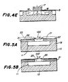
- a gate electrode 17 of polysilicon is deposited on the gate insulator film 15 by a CVD process and patterned subsequently such that the gate electrode 17 remains above the region 16 for a gate length L of 0,8 ⁇ m as shown in FIG.4E.
- This gate electrode 17 may be a lamination of polysilicon and silicide.
- the alignment between the patterned gate electrode 17 and the region 16 located below the gate electrode 17 can be achieved with an alignment accuracy within about 0.03 ⁇ m using the same stepper.
- ion implantation of arsenic (As + ) is made under an acceleration voltage of 60 keV for a dose of 5 X 10 15 cm -2 , and after a subsequent annealing, source and drain regions 18 are formed in the semiconductor layer 11. Further, by removing the silicon oxide film 15 from a region covering the source and drain regions 18, a MOS transistor shown in FIG.3 is completed wherein the source and drain regions 18 as well as a channel region 4 intervening therebetween are provided in the substrate 11 which in turn is provided on the insulator layer 10.
- the gate electrode extends between the source and drain regions 18 in a manner to cover a part of the source and drain regions 18 while the region 16 is provided immediately under the gate electrode 17 with a separation from the source and drain regions 18.
- This transistor is isolated from adjacent transistors by the isolation region 19 of silicon oxide which is formed already at the beginning of the process of FIG.4A.
- the size D of the window formed in the photoresist 13 is chosen such that the size D is smaller than the gate length L by 0.2 - 0.3 ⁇ m or more. As already described, the size D is set to 0.5 ⁇ m and the gate length L is set to 0.8 ⁇ m in the foregoing embodiment. By choosing the size D of the window as such, the region 16 remains invariably smaller than the gate electrode 17.
- the formation of unwanted p-n junction between the region 16 and the source or drain region 18, which otherwise would cause the decrease of the breakdown voltage, is eliminated because of the region 16 having a size smaller than the separation between the source and drain regions 18.
- the concentration of boron in such a contacting region can be held small and does not cause any substantial decrease of the breakdown voltage.
- FIGS.5A - 5E an embodiment of the present invention will be described with reference to FIGS.5A - 5E.
- the parts corresponding to the parts already described with reference to preceding drawings are given identical reference numerals and the description thereof will be omitted.
- a polysilicon layer 21 is deposited on the silicon layer 11 including the isolation region 19 for a thickness of 2000 - 3000 x 10 -10 m (2000 - 3000 ⁇ ) by a CVD process.
- the polysilicon layer 21 is doped with phosphorus (P) with a concentration determined such that the layer 21 has a surface resistivity of about 20 ⁇ / ⁇ .
- This layer 21 is used later as the source and drain regions of the MOS transistor.
- This layer 21 may be formed as a laminated structure of polysilicon and silicide.
- the doping may be made by ion implantation under an acceleration voltage of 50 keV, and a does of 5 X 10 15 cm -2 is used when phosphorus ions are doped. In the case of doping the polysilicon layer 21 by arsenic, the acceleration voltage is changed to 60 keV.
- a silicon oxide film 22 is deposited on the layer 21 by a low temperature CVD process at a temperature of 400°C for a thickness of 2000 x 10 -10 m (200 ⁇ ), and a part of the polysilicon layer 21 and the silicon oxide film 22 corresponding to the gate of the MOS transistor to be formed is removed by etching for a size L' to form an window 100.
- This size L' corresponds to the gate length of the desired MOS transistor.
- a silicon oxide layer 23 shown in FIG.5A by a broken line is deposited on the structure by a low temperature CVD process for 2000 x 10 -10 m (2000 ⁇ ) and the layer 23 is subsequently subjected to anisotropic etching process proceeding vertically to the surface of the layer 22 until the top surface of the substrate 11 is exposed in correspondence to the window L'.
- This anisotropic etching process may be performed by the reactive ion etching (RIE) process.
- RIE reactive ion etching
- FIG.5B is subjected to ion implantation of B + under an acceleration voltage of 30 - 40 keV with a dose of 3 X 10 13 cm -2 .
- the polysilicon layer 23 remaining at the side wall of the window 100' acts as the mask and the ion implantation is made only in correspondence to the window 100' having the size D' as shown in FIG.5C.
- the implanted boron ions reach a depth corresponding to the boundary between the single crystal silicon layer 11 and the insulator layer 10 underneath as illustrated therein.
- BF 2 may also be used as the ions to be implanted.
- a silicon oxide film 23 remaining in the structure of FIG.5C is removed completely, and a new silicon oxide film 24 is formed as shown in FIG.5D by thermal oxidation at 900 - 950°C under the existence of hydrochloride.
- This silicon oxide film 24 has a thickness of 200 x 10 -10 m (200 ⁇ ) for example and acts as the gate insulator film. It should be noted that during this thermal oxidation process, the oxidation proceeds more rapidly in the surface of the polysilicon layer 21 than in the surface of the single crystal silicon layer 11.
- the thickness of the silicon oxide layer 24 has a thickness of 4000-5000 x 10 -10 m (400 - 500 ⁇ ) at the side wall of the window which now has an increased size as illustrated by a reference numeral 100" as well as on the top surface of the layer 21, and because of this, a sufficient breakdown voltage is secured between the gate electrode and the polysilicon layer.
- FIG.5D shows the semiconductor device after the foregoing processes.
- a gate electrode 27 is provided in correspondence to the window 100".
- the window 100" has the size which is substantially identical to the size L' of the window 100, as the window 100" is smaller than the window 100 only by the thickness of the silicon oxide layer 24 which is, as already described, only about 400 - 500 x 10 -10 m (400 - 500 ⁇ ).
- the MOS transistor thus formed has the gate length which is substantially identical to the size L'.
- the region 25 for eliminating the back channel effect is separated from the source and drain regions 26.
- the p + -type region 25 does not form the p-n junction with the source or drain region 26 directly, and thereby the problem of unwanted decrease of the drain breakdown voltage is successfully eliminated.
Landscapes
- Thin Film Transistor (AREA)
Claims (3)
- Procédé pour fabriquer un dispositif métal-oxyde-semiconducteur ayant une structure semiconducteur-sur-isolant comprenant un substrat isolant (10) et un substrat de semiconducteur monocristallin (11) formé sur celui-ci, ledit substrat de semiconducteur monocristallin étant dopé par des premières impuretés pour avoir un premier type de conductibilité de manière à former une région de canal dans celui-ci, caractérisé en ce que ledit procédé comprend les étapes consistant à: former une couche de semiconducteur polycristallin (21) dopé par des deuxièmes impuretés pour avoir un deuxième type de conductibilité, opposé au premier type de conductibilité, sur une surface du substrat de semiconducteur semicristallin comme couche d'électrode du dispositif métal-oxyde-semiconducteur; former une ouverture (100) ayant une première dimension (L') dans la couche de semiconducteur polycristallin de telle manière qu'une surface supérieure du substrat de semiconducteur monocristallin soit exposée, ladite ouverture étant définie latéralement par une paroi latérale; exécuter un traitement d'implantation ionique pour introduire des troisièmes impuretés dudit premier type de conductibilité par l'ouverture en utilisant un masque avec une dose telle que lesdites troisièmes impuretés soient concentrées dans une région isolée (25) située à proximité d'une interface entre le substrat de semiconducteur monocristallin et le substrat isolant avec un niveau de concentration dépassant un niveau de concentration dudit substrat, ladite région isolée ayant une deuxième dimension plus petite que la première dimension; exécuter un traitement d'oxydation thermique de telle manière qu'une couche isolalnte de grille (24) soit formée sur la surface supérieure exposée du substrat de semiconducteur monocristallin et sur la paroi latérale de l'ouverture, ledit traitement d'oxydation thermique provoquant une diffusion des deuxièmes impuretés de la couche de semiconducteur polycristallin dans le substrat de semiconducteur monocristallin en formant par ce moyen des régions de source et de drain (26) dans le substrat de semiconducteur monocristallin, ledit traitement d'oxydation thermique provoquant en outre une activation des troisièmes impuretés dans la région isolée; et former une électrode de grille (27) en correspondance avec l'ouverture de telle manière que l'électrode de grille ait une longueur de grille plus grande que la deuxième dimension.
- Procédé selon la revendication 1, caractérisé en ce que ledit masque est formé par une étape consistant à former une première couche isolante (22) sur la couche de semiconducteur polycristallin, l'étape consistant à former l'ouverture (100) dans la première couche isolante et la couche de semiconducteur polycristallin, une étape consistant à déposer une deuxième couche isolante (23) sur la première couche comportant l'ouverture et la paroi latérale de telle manière que la surface supérieure exposée du substrat de semiconducteur monocristallin et la paroi latérale de l'ouverture soient recouvertes par la deuxième couche isolante, et une étape consistant à éliminer la deuxième couche isolante par un procédé d'attaque chimique anisotrope agissant verticalement par rapport à une surface prncipale de la deuxième couche isolante jusqu'à ce que la surface supérieure du substrat de semiconducteur monocristallin soit exposée, ledit traitement d'attaque chimique anisotrope étant exécuté de telle manière que la deuxième couche isolante soit laissée sur la paroi latérale de l'ouverture.
- Procédé selon la revendication 1, caractérisé en ce que lesdites premières impuretés et lesdites troisièmes impuretés sont identiques.
Applications Claiming Priority (2)
| Application Number | Priority Date | Filing Date | Title |
|---|---|---|---|
| JP1127501A JP2782781B2 (ja) | 1989-05-20 | 1989-05-20 | 半導体装置の製造方法 |
| JP127501/89 | 1989-05-20 |
Publications (2)
| Publication Number | Publication Date |
|---|---|
| EP0401577A1 EP0401577A1 (fr) | 1990-12-12 |
| EP0401577B1 true EP0401577B1 (fr) | 1996-12-27 |
Family
ID=14961535
Family Applications (1)
| Application Number | Title | Priority Date | Filing Date |
|---|---|---|---|
| EP90109511A Expired - Lifetime EP0401577B1 (fr) | 1989-05-20 | 1990-05-18 | Dispositif semi-conducteur métal-oxyde et sa méthode de fabrication |
Country Status (4)
| Country | Link |
|---|---|
| EP (1) | EP0401577B1 (fr) |
| JP (1) | JP2782781B2 (fr) |
| KR (1) | KR930008023B1 (fr) |
| DE (1) | DE69029485T2 (fr) |
Families Citing this family (5)
| Publication number | Priority date | Publication date | Assignee | Title |
|---|---|---|---|---|
| US5557126A (en) * | 1994-09-30 | 1996-09-17 | Sgs-Thomson Microelectronics, Inc. | Thin-film transistor and method for forming the same |
| GB2358079B (en) | 2000-01-07 | 2004-02-18 | Seiko Epson Corp | Thin-film transistor |
| GB2358080B (en) * | 2000-01-07 | 2004-06-02 | Seiko Epson Corp | Method of manufacturing a thin-film transistor |
| JP2007027201A (ja) * | 2005-07-12 | 2007-02-01 | Seiko Instruments Inc | 半導体装置の製造方法 |
| JP4987259B2 (ja) * | 2005-07-12 | 2012-07-25 | セイコーインスツル株式会社 | 半導体装置の製造方法 |
Family Cites Families (5)
| Publication number | Priority date | Publication date | Assignee | Title |
|---|---|---|---|---|
| JPS51135373A (en) * | 1975-05-20 | 1976-11-24 | Agency Of Ind Science & Technol | Semiconductor device |
| DE2641302A1 (de) * | 1976-09-14 | 1978-03-16 | Siemens Ag | N-kanal mis-fet in esfi-technik |
| JPS58139471A (ja) * | 1982-02-15 | 1983-08-18 | Fujitsu Ltd | Mis電界効果トランジスタ |
| JPS61127174A (ja) * | 1984-11-26 | 1986-06-14 | Toshiba Corp | 半導体装置の製造方法 |
| JPS63114266A (ja) * | 1986-10-31 | 1988-05-19 | Fujitsu Ltd | 半導体装置の製造方法 |
-
1989
- 1989-05-20 JP JP1127501A patent/JP2782781B2/ja not_active Expired - Lifetime
-
1990
- 1990-05-18 DE DE69029485T patent/DE69029485T2/de not_active Expired - Fee Related
- 1990-05-18 EP EP90109511A patent/EP0401577B1/fr not_active Expired - Lifetime
- 1990-05-21 KR KR9007273A patent/KR930008023B1/ko not_active Expired - Fee Related
Also Published As
| Publication number | Publication date |
|---|---|
| JP2782781B2 (ja) | 1998-08-06 |
| DE69029485T2 (de) | 1997-04-10 |
| KR930008023B1 (en) | 1993-08-25 |
| EP0401577A1 (fr) | 1990-12-12 |
| JPH02306665A (ja) | 1990-12-20 |
| KR900019128A (ko) | 1990-12-24 |
| DE69029485D1 (de) | 1997-02-06 |
Similar Documents
| Publication | Publication Date | Title |
|---|---|---|
| US6518623B1 (en) | Semiconductor device having a buried-channel MOS structure | |
| US4637124A (en) | Process for fabricating semiconductor integrated circuit device | |
| US6147383A (en) | LDD buried channel field effect semiconductor device and manufacturing method | |
| US5849616A (en) | Method of manufacturing a semiconductor device | |
| US4935379A (en) | Semiconductor device and method of manufacturing the same | |
| EP0480635A1 (fr) | Transistor couche mince et méthode de fabrication | |
| EP0248292B1 (fr) | Dispositif semi-conducteur à haute tension de claquage | |
| US6599782B1 (en) | Semiconductor device and method of fabricating thereof | |
| EP0382165B1 (fr) | Dispositif semi-conducteur à haute tension ayant une structure de type silicium sur isolant avec une résistance à l'état conducteur réduite | |
| US4507846A (en) | Method for making complementary MOS semiconductor devices | |
| US5238857A (en) | Method of fabricating a metal-oxide-semiconductor device having a semiconductor on insulator (SOI) structure | |
| US5291049A (en) | Mosfet with buried element isolation regions | |
| US5128739A (en) | MIS type semiconductor device formed in a semiconductor substrate having a well region | |
| US5242849A (en) | Method for the fabrication of MOS devices | |
| JPH07122657A (ja) | 半導体メモリとその製法 | |
| US4517731A (en) | Double polysilicon process for fabricating CMOS integrated circuits | |
| EP0337823A2 (fr) | Transistor à effet de champ ayant une tension de claquage élevée | |
| EP0308612A2 (fr) | Transistor à effet de champ et procédé pour sa fabrication | |
| EP0401577B1 (fr) | Dispositif semi-conducteur métal-oxyde et sa méthode de fabrication | |
| US5521416A (en) | Semiconductor device having gate electrode and impurity diffusion layer different in conductivity type and method of manufacturing the same | |
| JPH07153952A (ja) | 半導体装置及びその製造方法 | |
| JP3106757B2 (ja) | Mos電界効果半導体装置の製造方法 | |
| JP2729422B2 (ja) | 半導体装置 | |
| EP0615288A2 (fr) | Procédé de fabrication d'un dispositif semi-conducteur comportant une région d'isolation | |
| JPH09223797A (ja) | 半導体装置の製造方法 |
Legal Events
| Date | Code | Title | Description |
|---|---|---|---|
| PUAI | Public reference made under article 153(3) epc to a published international application that has entered the european phase |
Free format text: ORIGINAL CODE: 0009012 |
|
| AK | Designated contracting states |
Kind code of ref document: A1 Designated state(s): DE FR GB |
|
| 17P | Request for examination filed |
Effective date: 19901228 |
|
| 17Q | First examination report despatched |
Effective date: 19930201 |
|
| GRAG | Despatch of communication of intention to grant |
Free format text: ORIGINAL CODE: EPIDOS AGRA |
|
| GRAH | Despatch of communication of intention to grant a patent |
Free format text: ORIGINAL CODE: EPIDOS IGRA |
|
| GRAH | Despatch of communication of intention to grant a patent |
Free format text: ORIGINAL CODE: EPIDOS IGRA |
|
| GRAA | (expected) grant |
Free format text: ORIGINAL CODE: 0009210 |
|
| AK | Designated contracting states |
Kind code of ref document: B1 Designated state(s): DE FR GB |
|
| REF | Corresponds to: |
Ref document number: 69029485 Country of ref document: DE Date of ref document: 19970206 |
|
| ET | Fr: translation filed | ||
| PLBE | No opposition filed within time limit |
Free format text: ORIGINAL CODE: 0009261 |
|
| STAA | Information on the status of an ep patent application or granted ep patent |
Free format text: STATUS: NO OPPOSITION FILED WITHIN TIME LIMIT |
|
| 26N | No opposition filed | ||
| REG | Reference to a national code |
Ref country code: GB Ref legal event code: IF02 |
|
| PGFP | Annual fee paid to national office [announced via postgrant information from national office to epo] |
Ref country code: DE Payment date: 20060511 Year of fee payment: 17 |
|
| PGFP | Annual fee paid to national office [announced via postgrant information from national office to epo] |
Ref country code: FR Payment date: 20060515 Year of fee payment: 17 |
|
| PGFP | Annual fee paid to national office [announced via postgrant information from national office to epo] |
Ref country code: GB Payment date: 20060517 Year of fee payment: 17 |
|
| GBPC | Gb: european patent ceased through non-payment of renewal fee |
Effective date: 20070518 |
|
| REG | Reference to a national code |
Ref country code: FR Ref legal event code: ST Effective date: 20080131 |
|
| PG25 | Lapsed in a contracting state [announced via postgrant information from national office to epo] |
Ref country code: DE Free format text: LAPSE BECAUSE OF NON-PAYMENT OF DUE FEES Effective date: 20071201 |
|
| PG25 | Lapsed in a contracting state [announced via postgrant information from national office to epo] |
Ref country code: GB Free format text: LAPSE BECAUSE OF NON-PAYMENT OF DUE FEES Effective date: 20070518 |
|
| PG25 | Lapsed in a contracting state [announced via postgrant information from national office to epo] |
Ref country code: FR Free format text: LAPSE BECAUSE OF NON-PAYMENT OF DUE FEES Effective date: 20070531 |