EP0401852A2 - Oberflächenmikroskop - Google Patents
Oberflächenmikroskop Download PDFInfo
- Publication number
- EP0401852A2 EP0401852A2 EP90110884A EP90110884A EP0401852A2 EP 0401852 A2 EP0401852 A2 EP 0401852A2 EP 90110884 A EP90110884 A EP 90110884A EP 90110884 A EP90110884 A EP 90110884A EP 0401852 A2 EP0401852 A2 EP 0401852A2
- Authority
- EP
- European Patent Office
- Prior art keywords
- sample
- signal
- microscope according
- probe
- surface microscope
- Prior art date
- Legal status (The legal status is an assumption and is not a legal conclusion. Google has not performed a legal analysis and makes no representation as to the accuracy of the status listed.)
- Granted
Links
Images


Classifications
-
- G—PHYSICS
- G01—MEASURING; TESTING
- G01Q—SCANNING-PROBE TECHNIQUES OR APPARATUS; APPLICATIONS OF SCANNING-PROBE TECHNIQUES, e.g. SCANNING PROBE MICROSCOPY [SPM]
- G01Q30/00—Auxiliary means serving to assist or improve the scanning probe techniques or apparatus, e.g. display or data processing devices
- G01Q30/04—Display or data processing devices
-
- B—PERFORMING OPERATIONS; TRANSPORTING
- B82—NANOTECHNOLOGY
- B82Y—SPECIFIC USES OR APPLICATIONS OF NANOSTRUCTURES; MEASUREMENT OR ANALYSIS OF NANOSTRUCTURES; MANUFACTURE OR TREATMENT OF NANOSTRUCTURES
- B82Y35/00—Methods or apparatus for measurement or analysis of nanostructures
-
- G—PHYSICS
- G01—MEASURING; TESTING
- G01Q—SCANNING-PROBE TECHNIQUES OR APPARATUS; APPLICATIONS OF SCANNING-PROBE TECHNIQUES, e.g. SCANNING PROBE MICROSCOPY [SPM]
- G01Q60/00—Particular types of SPM [Scanning Probe Microscopy] or microscopes; Essential components thereof
- G01Q60/10—STM [Scanning Tunnelling Microscopy] or apparatus therefor, e.g. STM probes
- G01Q60/12—STS [Scanning Tunnelling Spectroscopy]
-
- Y—GENERAL TAGGING OF NEW TECHNOLOGICAL DEVELOPMENTS; GENERAL TAGGING OF CROSS-SECTIONAL TECHNOLOGIES SPANNING OVER SEVERAL SECTIONS OF THE IPC; TECHNICAL SUBJECTS COVERED BY FORMER USPC CROSS-REFERENCE ART COLLECTIONS [XRACs] AND DIGESTS
- Y10—TECHNICAL SUBJECTS COVERED BY FORMER USPC
- Y10S—TECHNICAL SUBJECTS COVERED BY FORMER USPC CROSS-REFERENCE ART COLLECTIONS [XRACs] AND DIGESTS
- Y10S977/00—Nanotechnology
- Y10S977/84—Manufacture, treatment, or detection of nanostructure
- Y10S977/849—Manufacture, treatment, or detection of nanostructure with scanning probe
- Y10S977/852—Manufacture, treatment, or detection of nanostructure with scanning probe for detection of specific nanostructure sample or nanostructure-related property
-
- Y—GENERAL TAGGING OF NEW TECHNOLOGICAL DEVELOPMENTS; GENERAL TAGGING OF CROSS-SECTIONAL TECHNOLOGIES SPANNING OVER SEVERAL SECTIONS OF THE IPC; TECHNICAL SUBJECTS COVERED BY FORMER USPC CROSS-REFERENCE ART COLLECTIONS [XRACs] AND DIGESTS
- Y10—TECHNICAL SUBJECTS COVERED BY FORMER USPC
- Y10S—TECHNICAL SUBJECTS COVERED BY FORMER USPC CROSS-REFERENCE ART COLLECTIONS [XRACs] AND DIGESTS
- Y10S977/00—Nanotechnology
- Y10S977/84—Manufacture, treatment, or detection of nanostructure
- Y10S977/849—Manufacture, treatment, or detection of nanostructure with scanning probe
- Y10S977/86—Scanning probe structure
- Y10S977/861—Scanning tunneling probe
Definitions
- the present invention relates to a surface microscope utilizing tunnel current or field emission current produced when a probe is brought close to a sample, and in particular to a surface microscope suitable for measuring tunnel barrier (tunneling barrier height), by means of which it is possible to find an interface, at which physical properties change at the neighborhood of the surface of the sample, e.g. an interface between the p type semiconductivity and the n type semiconductivity region at the surface of a semiconductor body, by measuring the tunnel barrier at the surface of the sample.
- tunnel barrier tunnel barrier height
- ⁇ 1 ⁇ 2 ⁇ (ln J T )/ ⁇ S (1) That is, ⁇ 1 ⁇ 2 can be measured, based on the tunnel current density J T and variations ⁇ S in the gap between the probe and the sample. Between them, ⁇ S can be set by vibrating the probe. J T is obtained by dividing the intensity of the tunnel current by the current emission area. However the emission area is not known at all. Further, the current density J T is varied also by absolute variations of the gap.
- the object of the present invention is to provide a surface microscope capable of measuring distribution of the tunnel barrier ( ⁇ ) at the surface of the sample with a high precision.
- ⁇ I -k2 ⁇ 1 ⁇ 2 ⁇ S (4)
- ⁇ 1 ⁇ 2 can be expressed, as given by Eq.
- ⁇ 1 ⁇ 2 -( )( ⁇ I I ) (5)
- the tunnel barrier information measuring means can be combined with a scanning tunneling microscope (STM) measuring the superficial shape of the sample by using tunnel current or an apparatus similar to the STM measuring the superficial shape of the sample by using the force acting between the probe and the sample, the electrostatic capacitance, heat, light, sound, etc. so that information on the shape and the tunnel barrier information can be measured simultaneously.
- the display system displaying obtained information can be so constructed that the information on the superficial shape of the sample described about and the ⁇ 1 ⁇ 2 (or ⁇ ) information are displayed on a same screen, superposed on each other.
- a display system and a display method capable of dealing with a large amount of data or a number of kinds of data can be adopted.
- the probe 1 is brought close and opposite to the surface of the sample 2. It is so constructed that it is vibrated with an amplitude of ⁇ S in the Z axis direction of a piezo element 3.
- a bias power supply 9 supplies a bias voltage through the probe 1 and the sample 2.
- the tunnel current I flowing through the probe 1 and the sample 2 is modulated by the vibration of the probe 1 and detected by a current detector 4.
- a current setting circuit 8 is a circuit for setting the DC component of the tunnel current I.
- the position of the probe 1 in the height in the Z axis direction is controlled by a servo mechanism so that the tunnel current I has a current intensity set by the current setting circuit 8, when the surface of the sample is scanned with the probe 1.
- the difference between the tunnel current I detected by the current detector 4 and the current set by the current setting circuit 8 is formed in an error detector 5 and variations ⁇ I in the tunnel current I are detected.
- a divider 6 divides the variations ⁇ I in the tunnel current coming from the error detector 5 by the tunnel current I from the current detector 4.
- a lock-in amplifier 7 includes an oscillator and outputs a vibrating signal S v for giving the piezo element 3 vibration. At the same time it takes out a ⁇ I/I component synchronized with the frequency of the vibrating S v or having a predetermined phase difference with respect thereto from the output signal from the divider 6 and outputs it to a multiplier 25.
- the vibrating signal S v is transformed into an amplitude ⁇ S of the vibration of the probe 1 by a transforming circuit 26 on the basis of electrostriction characteristics of the piezo element 3 and transformed further into a value of 1/(k2 ⁇ S).
- the multiplier 25 multiplies the output 1/(k2 ⁇ S) of the transforming circuit 26 by the output AI/I of the lock-in amplifier 7 and thus ⁇ 1 ⁇ 2 is calculated according to Eq. (5) described above.
- the probe 1 and the sample 2 should be so close to each other that the distance therebetween is about 10 ⁇ . In this way it is possible to obtain information on the tunnel barrier ( ⁇ ) or the square root of the tunnel barrier ( ⁇ 1 ⁇ 2 ) .
- Fig. 2 there are indicated, apart from the construction indicated in Fig. 1, also a constant current servo system for obtaining an STM image, which is a three-dimensional surface construction image of the surface of the sample and a data processing and displaying section.
- the constant current servo system is a system, which controls the tunnel current flowing through the probe during the scanning so as to be a constant current, when the surface of the sample 2 is two-dimensionally scanned with the probe 1, and consists of the current detector 4 connected in series with the bias power supply 9, the error current detecting circuit 5, the divider 6, a PI controlling section 10, an adding circuit 11 and a high voltage amplifier 12.
- the vibrating signal S v for vibrating the probe 1 is superposed on the servo signal. In this way, apart from the servo signal, the vibrating signal S v is applied to the Z axis piezo element to give the probe 1 vibration so that the tunnel gap g is varied with an amplitude of ⁇ S.
- the tunnel current i t flowing between the probe 1 and the sample 2 has a DC component approximately stabilized at a specified current intensity 5 and an AC component due to the vibration of the probe 1.
- This AC component ⁇ I is detected by the error detector and transformed into a ⁇ I/I signal, which is inputted in the lock-in amplifier 7.
- the lock-in amplifier 7 takes out the ⁇ I/I component, which is synchronized with the vibrating frequency of the vibrating signal S v or deviated by a predetermined phase therefrom, and sends it to the multiplier 25.
- the multiplier 25 forms the product of the signal 1/(K2 ⁇ S) coming from the transforming circuit 26 and the signal ⁇ I/I coming from the lock-in amplifier 7 to obtain the ⁇ 1 ⁇ 2 information, which is stored in an image memorizing section 17.
- the signal close to the DC component of the divider 6 represents an error from the tunnel gap corresponding to the aimed current intensity.
- An output signal is formed by a PI control section 10 so that the error becomes zero and the position of the probe 1 in the Z axis direction is constant-current-servo controlled through the adding circuit 11 and the high voltage amplifier 12. Owing to this constant-current-servo control operation the probe 1 is moved two-dimensionally along fine unevenness on the surface of the sample. Consequently the output signal of the PI control section 10 represents information on the surface of the sample in the height (Z-axis) direction. This signal is stored in the image memorizing section 16.
- the PI control section 10 consists of a proportional member and an integral member connected in series or parallel, whose frequency region is extended so as to be able to servo the probe up to a higher frequency region than a control system composed only of an integrator.
- a control system including only an integrator or a PID control system including further a differential member can be applied also to the control system in the present embodiment. Still further, from the stand point of obtaining the ⁇ 1 ⁇ 2 information and the height information simultaneously, it is desirable that the frequency response region of the constant-current-servo system is lower than the vibrating frequency coming from the lock-in amplifier 7.
- an X- and a Y-scanning signal are inputted from the two-dimensional scanning section 15 in an X axis piezo element and a Y axis piezo element 14, respectively and at the same time they are inputted also in the image memorizing sections 16 and 17, respectively, as address information.
- the two-dimensional scanning section 15 has, as usually known, an X and a Y counter counting clocks from a clock generator so as to adapt it to the X axis and the Y axis scanning, terminals, through which the outputs of these counters are outputted as addresses of X and Y, respectively, and terminals, through which they are outputted to the X axis and the Y axis piezo elements 13 and 14, respectively, after having DA converted the outouts of these counters.
- the surface of the sample is raster-scanned with the probe 1 by means of the X axis and the Y axis piezo element 13 and 14 driven by the X and the Y scanning signal, respectively, and in this way it is possible to obtain the ⁇ 1 ⁇ 2 information together with the three-dimensional shape information on the surface of the sample by using the (X, Y) addresses and the height information.
- the sample 2 instead of the three-dimensional movement of the probe, the sample 2 may be moved three-dimensionally or the probe and the sample may bear their share of the moving means. What is essential is that the probe 1 and the sample 2 are displaced three-dimensionally with respect to each other.
- the three-dimensional shape information is stored in the image memorizing section 16, while the two-dimensional information on ⁇ 1 ⁇ 2 is stored in the image memorizing section 17.
- the data either one of the signals is displayed in a VTR 19 or a TV monitor 20 as a brightness modulated image of the height information or the ⁇ 1 ⁇ 2 information.
- the obtained data may be subjected to data processing for effecting a contour line display, a shadow processing display or a steroscopic display other than the display similar to that described above. Still further it is possible also to subject the obtained data to FET (fast Fourier transformation) processing, smoothing processing, etc. or to enable base line regulation, gain regulation, further window processing (partial enlargement, partial processing), cross-sectional display between two points of specified coordinate. Furthermore, since the display device in the computer is not of high quality, it is desirable to use the TV monitor 20 or the CRT monitor 21 also for displaying the data processed by means of the computer.
- FET fast Fourier transformation
- the method is the most advantageous, by which the data processed by means of the computer are stored once again in either one of the image memorizing sections 16 and 17 through lines 16a and 17a, respectively, and they are displayed thereafter.
- an image memorizing section (not shown in the figure) exclusively used therefor. In a practical mounting either one of them may be used.
- the VTR may be either analogue or digital. However there can be a case where it is desired to deal with these raw data by means of the computer.
- the signal of the VTR 19 is inputted in the computer through an interface 29 used exclusively for the VTR and displayed with TV monitor 20 and the CRT monitor 21 through the image memorizing section according to the procedure described above after the data processing.
- data which should be conserved, may be stored in the VTR 19 or in the memory of the computer 18.
- Fig. 3 shows an example, in which the present invention is applied to an atomic force microscope.
- the mechanism section consists of detecting sections 30 and 31 detecting a constant atomic force (repulsive or attractive force between atoms at the extremity of the probe 30 and atoms on the sample), a tripod type scanner 32 controlling the sample three-dimensionally and a rough regulation mechanism 33 having a function of the visual field selection and a function of bringing the prove close to the sample.
- the detecting system is composed of the probe 30 consisting of a cantilever 30′, whose extremity is covered by a conductive section 30 ⁇ as indicated in the figure, and a non-contact type displacement meter (cantilever deflection detector) 31 for measuring the cantilever displacements thereof with a high precision to detect the force.
- a meter, to which the principle of the scanning tunneling microscope is applied, or a capacity type displacement meter, a laser interfero-meter, etc. on the market is conceivable for this non-contact type displacement meter 31 used at this time.
- the tripod type scanner 32 combines the Z axis the X axis and the Y axis piezo-element 3, 13, 14 to control the sample 2 through a sample table 37, as indicated in the figure.
- the mechanism is so constructed that the sample is three-dimensionally controlled, which is reverse with respect to the mechanism by the method, by which the probe 1 is three-dimensionally controlled, as indicated in Fig. 2.
- the sample table 37 should be made
- the sample 2 is brought close to the probe 30 by using a well-known rough regulation mechanism mounted on a base 34.
- a servo system 36 an adding circuit 11, a high voltage amplifier 12, and the Z axis piezo element 3 are driven.
- the probe 30 should not collide with the sample 2, when they are brought rapidly close to each other.
- the elements described above are driven so that the two-dimensional scanning is effected, while keeping the detected force at a desired value.
- the object of the present invention can be achieved by combining the shape measuring means using the probe with means for measuring the tunnel barrier ( ⁇ 1 ⁇ 2 ) information as in the embodiment indicated in Fig. 1. Concretely speaking, apart from the device utilizing the tunnel current indicated in Fig. 2 and the device utilizing the atomic force indicated in Fig.
- the ⁇ 1 ⁇ 2 information measuring means may be combined with another well known superficial shape measuring device utilizing electrostatic capacitance, light, heat and sound. Further it is also in the scope of the present invention to measure the tunnel current, while irradiating the sample 2 with radiation (X-ray, ultraviolet ray, laser light, visible light and infrared ray) by using optical means such as an optical fiber 38 and a focusing lens 39, etc.
- radiation X-ray, ultraviolet ray, laser light, visible light and infrared ray
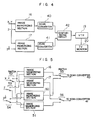
- Fig. 4 shows a concrete example for realizing a display formalism more easily understood of the tunnel barrier ( ⁇ ) or ⁇ 1 ⁇ 2 information and the height information thus obtained.
- image information obtained in the manner, as indicated in Fig. 2 is displayed in a TV monitor 20 by taking out analogue image signals from the image memorizing sections 16 and 17 through scan converters 40 and 41, respectively, and converting them into color image signals in a synthesizing circuit 42.
- very useful information can be obtained, because the distribution of the tunnel barrier ⁇ 1 ⁇ 2 can be known simultaneously together with the fine structure of the surface, e.g. if shape information of the surface is displayed in green and the ⁇ 1 ⁇ 2 information in red.
- FIG. 4 there are disposed image memorizing sections 50 and 51 and further switches 52, 53 and 54 on the data input side as well as switches 55 and 56 on the data output side.
- the figure shows a state, where during a period of time where the three-dimensional shape information is recorded in the image memorizing section 50 and the ⁇ 1 ⁇ 2 information in the image memorizing section 51, information stored previously in the image memorizing section 16 and that stored previously in the image memorizing section 17 are transmitted to the scan converters 40 and 41, respectively.
- the switches 52 to 56 are switched over to the respective contacts on the opposite side and recording is effected again in the image memorizing sections 16 and 17.
- the display is effected by outputting the memory contents in the image memorizing sections 50 and 51.
- this example concerns the combinations of the height information with the ⁇ 1 ⁇ 2 information, combinations of other physical quantities such as tunnel current, capacitance, sound, light, heat, force, etc. and further combinations of more than two of them are conceivable.
- the present invention can be applied to the case of the display only of the three-dimensional shape information (STM image). These don't depart from the scope of the present invention.
- the present invention since it is possible to measure the three-dimensional shape of the surface of the sample and at the same time to measure the distribution of the tunnel barrier ( ⁇ ) or ⁇ 1 ⁇ 2 on a surface, even if the surface is composed of different kinds of elements, it is possible to distinguish them. Further, according to the present invention, since it is possible to obtain data at the same time as a usual surface measurement, the measurement can be effected in an extremely short time with respect to the tunnel electron spectroscopy using tunnel current. Since the measurement can be effected in a time shorter than a half of the time required by the method using the tunnel current, influences of the drift of the sample are reduced, which is advantageous. Furthermore, since concerning the tunnel current at the measurement the measurement can be executed with a very small current with respect to that required by the tunnel electron spectroscopy, it is possible to obtain data very stably.
Landscapes
- Physics & Mathematics (AREA)
- Radiology & Medical Imaging (AREA)
- Health & Medical Sciences (AREA)
- General Health & Medical Sciences (AREA)
- General Physics & Mathematics (AREA)
- Nuclear Medicine, Radiotherapy & Molecular Imaging (AREA)
- Chemical & Material Sciences (AREA)
- Spectroscopy & Molecular Physics (AREA)
- Engineering & Computer Science (AREA)
- Nanotechnology (AREA)
- Analytical Chemistry (AREA)
- Crystallography & Structural Chemistry (AREA)
- Measurement Of Length, Angles, Or The Like Using Electric Or Magnetic Means (AREA)
- Testing Or Calibration Of Command Recording Devices (AREA)
Applications Claiming Priority (2)
| Application Number | Priority Date | Filing Date | Title |
|---|---|---|---|
| JP145329/89 | 1989-06-09 | ||
| JP1145329A JP2880182B2 (ja) | 1989-06-09 | 1989-06-09 | 表面顕微鏡 |
Publications (3)
| Publication Number | Publication Date |
|---|---|
| EP0401852A2 true EP0401852A2 (de) | 1990-12-12 |
| EP0401852A3 EP0401852A3 (de) | 1992-12-09 |
| EP0401852B1 EP0401852B1 (de) | 1995-10-04 |
Family
ID=15382651
Family Applications (1)
| Application Number | Title | Priority Date | Filing Date |
|---|---|---|---|
| EP90110884A Expired - Lifetime EP0401852B1 (de) | 1989-06-09 | 1990-06-08 | Oberflächenmikroskop |
Country Status (4)
| Country | Link |
|---|---|
| US (1) | US5036196A (de) |
| EP (1) | EP0401852B1 (de) |
| JP (1) | JP2880182B2 (de) |
| DE (1) | DE69022777T2 (de) |
Cited By (1)
| Publication number | Priority date | Publication date | Assignee | Title |
|---|---|---|---|---|
| GB2267761A (en) * | 1992-06-02 | 1993-12-15 | Hitachi Europ Ltd | Electrically testing a sample |
Families Citing this family (13)
| Publication number | Priority date | Publication date | Assignee | Title |
|---|---|---|---|---|
| US5289004A (en) * | 1990-03-27 | 1994-02-22 | Olympus Optical Co., Ltd. | Scanning probe microscope having cantilever and detecting sample characteristics by means of reflected sample examination light |
| US5193383A (en) * | 1990-07-11 | 1993-03-16 | The United States Of America As Represented By The Secretary Of The Navy | Mechanical and surface force nanoprobe |
| US5186041A (en) * | 1990-11-28 | 1993-02-16 | International Business Machines Corporation | Microprobe-based CD measurement tool |
| US5329122A (en) * | 1991-08-29 | 1994-07-12 | Canon Kabushiki Kaisha | Information processing apparatus and scanning tunnel microscope |
| US5336887A (en) * | 1991-11-15 | 1994-08-09 | Olympus Optical Co., Ltd. | Scanning probe microscope |
| DE69309318T2 (de) * | 1992-01-10 | 1997-10-30 | Hitachi, Ltd., Tokio/Tokyo | Verfahren und Vorrichtung zum Beobachten einer Fläche |
| DE69522241T2 (de) * | 1995-05-13 | 2002-05-02 | International Business Machines Corp., Armonk | Datenerfassungs- und steueranlage für rastenprobenmikroskop |
| US5874668A (en) * | 1995-10-24 | 1999-02-23 | Arch Development Corporation | Atomic force microscope for biological specimens |
| JP2952327B2 (ja) * | 1997-07-16 | 1999-09-27 | セイコーインスツルメンツ株式会社 | 走査型プローブ顕微鏡 |
| DE19754681A1 (de) * | 1997-12-10 | 1999-06-17 | Peter Heiland | In einem Rastermodus abtastende Vorrichtung mit einer Kompensation des Störeinflusses vonmechanischen Schwingungen auf dem Abtastvorgang |
| US6953930B2 (en) * | 2001-08-27 | 2005-10-11 | Nippon Telegraph And Telephone Corporation | Conductive transparent probe and probe control apparatus |
| JP5809850B2 (ja) * | 2011-06-01 | 2015-11-11 | オリンパス株式会社 | 画像処理装置 |
| US10495665B2 (en) * | 2016-09-19 | 2019-12-03 | Zyvex Labs, Llc | Methods, devices and systems for scanning tunneling microscopy control system design |
Family Cites Families (6)
| Publication number | Priority date | Publication date | Assignee | Title |
|---|---|---|---|---|
| CH643397A5 (de) * | 1979-09-20 | 1984-05-30 | Ibm | Raster-tunnelmikroskop. |
| US4747698A (en) * | 1986-04-30 | 1988-05-31 | International Business Machines Corp. | Scanning thermal profiler |
| JPS643502A (en) * | 1987-06-25 | 1989-01-09 | Seiko Instr & Electronics | Scanning type tunnel microscope |
| DE3853155T2 (de) * | 1987-10-09 | 1995-06-14 | Hitachi Ltd | Rastertunnelmikroskop mit einer Vorrichtung zum Berichtigen von Oberflächendaten. |
| US4823004A (en) * | 1987-11-24 | 1989-04-18 | California Institute Of Technology | Tunnel and field effect carrier ballistics |
| US4870352A (en) * | 1988-07-05 | 1989-09-26 | Fibertek, Inc. | Contactless current probe based on electron tunneling |
-
1989
- 1989-06-09 JP JP1145329A patent/JP2880182B2/ja not_active Expired - Fee Related
-
1990
- 1990-06-05 US US07/533,341 patent/US5036196A/en not_active Expired - Lifetime
- 1990-06-08 DE DE69022777T patent/DE69022777T2/de not_active Expired - Fee Related
- 1990-06-08 EP EP90110884A patent/EP0401852B1/de not_active Expired - Lifetime
Cited By (2)
| Publication number | Priority date | Publication date | Assignee | Title |
|---|---|---|---|---|
| GB2267761A (en) * | 1992-06-02 | 1993-12-15 | Hitachi Europ Ltd | Electrically testing a sample |
| GB2267761B (en) * | 1992-06-02 | 1996-01-17 | Hitachi Europ Ltd | Method of electrically testing a sample |
Also Published As
| Publication number | Publication date |
|---|---|
| DE69022777D1 (de) | 1995-11-09 |
| JPH0312503A (ja) | 1991-01-21 |
| US5036196A (en) | 1991-07-30 |
| DE69022777T2 (de) | 1996-03-14 |
| EP0401852B1 (de) | 1995-10-04 |
| JP2880182B2 (ja) | 1999-04-05 |
| EP0401852A3 (de) | 1992-12-09 |
Similar Documents
| Publication | Publication Date | Title |
|---|---|---|
| EP0401852B1 (de) | Oberflächenmikroskop | |
| US5210410A (en) | Scanning probe microscope having scan correction | |
| EP0410131B1 (de) | Nah-Feld Lorentz-Kraft-Mikroskopie | |
| USRE34331E (en) | Feedback control for scanning tunnel microscopes | |
| EP0347739B1 (de) | Rastertunnelmikroskop und Verfahren zur topographischen Untersuchung einer Oberfläche | |
| Barrett et al. | Optical scan‐correction system applied to atomic force microscopy | |
| Horcas et al. | WSXM: A software for scanning probe microscopy and a tool for nanotechnology | |
| US5168159A (en) | Barrier height measuring apparatus including a conductive cantilever functioning as a tunnelling probe | |
| US5466935A (en) | Programmable, scanned-probe microscope system and method | |
| US5939715A (en) | Scanning probe microscope | |
| US5336887A (en) | Scanning probe microscope | |
| US5260572A (en) | Scanning probe microscope including height plus deflection method and apparatus to achieve both high resolution and high speed scanning | |
| EP0422449B1 (de) | Potentiospektroskopisches Rastertunnelmikroskop und Datenerfassungsmethode | |
| JP3070216B2 (ja) | 表面顕微鏡及び顕微方法 | |
| EP0408009B1 (de) | Tunnelspektroskop und Verfahren zur Gewinnung von spektroskopischer Information | |
| JP3131517B2 (ja) | 走査型プローブ顕微鏡装置 | |
| JP3451620B2 (ja) | 信号処理方法および走査型プローブ顕微鏡 | |
| JP3377918B2 (ja) | 走査型プローブ顕微鏡 | |
| JP3058724B2 (ja) | 走査型プローブ顕微鏡 | |
| JPH0712824A (ja) | 電位分布測定機能を備える走査型トンネル顕微鏡 | |
| JPH05340712A (ja) | 走査型プローブ顕微鏡リアルタイム表示装置 | |
| JP2713717B2 (ja) | 走査型プローブ顕微鏡 | |
| JP3121619B2 (ja) | 走査型トンネル顕微鏡の画像処理方法 | |
| JP3029504B2 (ja) | 走査型トンネル顕微鏡および情報記録再生装置 | |
| JPH09264897A (ja) | 走査型プローブ顕微鏡 |
Legal Events
| Date | Code | Title | Description |
|---|---|---|---|
| PUAI | Public reference made under article 153(3) epc to a published international application that has entered the european phase |
Free format text: ORIGINAL CODE: 0009012 |
|
| 17P | Request for examination filed |
Effective date: 19900608 |
|
| AK | Designated contracting states |
Kind code of ref document: A2 Designated state(s): DE FR GB |
|
| PUAL | Search report despatched |
Free format text: ORIGINAL CODE: 0009013 |
|
| AK | Designated contracting states |
Kind code of ref document: A3 Designated state(s): DE FR GB |
|
| 17Q | First examination report despatched |
Effective date: 19941230 |
|
| GRAA | (expected) grant |
Free format text: ORIGINAL CODE: 0009210 |
|
| AK | Designated contracting states |
Kind code of ref document: B1 Designated state(s): DE FR GB |
|
| REF | Corresponds to: |
Ref document number: 69022777 Country of ref document: DE Date of ref document: 19951109 |
|
| ET | Fr: translation filed | ||
| PLBE | No opposition filed within time limit |
Free format text: ORIGINAL CODE: 0009261 |
|
| STAA | Information on the status of an ep patent application or granted ep patent |
Free format text: STATUS: NO OPPOSITION FILED WITHIN TIME LIMIT |
|
| 26N | No opposition filed | ||
| REG | Reference to a national code |
Ref country code: GB Ref legal event code: IF02 |
|
| PGFP | Annual fee paid to national office [announced via postgrant information from national office to epo] |
Ref country code: GB Payment date: 20040526 Year of fee payment: 15 Ref country code: FR Payment date: 20040526 Year of fee payment: 15 |
|
| PGFP | Annual fee paid to national office [announced via postgrant information from national office to epo] |
Ref country code: DE Payment date: 20040608 Year of fee payment: 15 |
|
| PG25 | Lapsed in a contracting state [announced via postgrant information from national office to epo] |
Ref country code: GB Free format text: LAPSE BECAUSE OF NON-PAYMENT OF DUE FEES Effective date: 20050608 |
|
| PG25 | Lapsed in a contracting state [announced via postgrant information from national office to epo] |
Ref country code: DE Free format text: LAPSE BECAUSE OF NON-PAYMENT OF DUE FEES Effective date: 20060103 |
|
| PG25 | Lapsed in a contracting state [announced via postgrant information from national office to epo] |
Ref country code: FR Free format text: LAPSE BECAUSE OF NON-PAYMENT OF DUE FEES Effective date: 20060228 |
|
| GBPC | Gb: european patent ceased through non-payment of renewal fee |
Effective date: 20050608 |
|
| REG | Reference to a national code |
Ref country code: FR Ref legal event code: ST Effective date: 20060228 |