EP0401960A2 - Ordinateur avec un connecteur pour une carte d'extension - Google Patents
Ordinateur avec un connecteur pour une carte d'extension Download PDFInfo
- Publication number
- EP0401960A2 EP0401960A2 EP90302924A EP90302924A EP0401960A2 EP 0401960 A2 EP0401960 A2 EP 0401960A2 EP 90302924 A EP90302924 A EP 90302924A EP 90302924 A EP90302924 A EP 90302924A EP 0401960 A2 EP0401960 A2 EP 0401960A2
- Authority
- EP
- European Patent Office
- Prior art keywords
- high speed
- processing apparatus
- data processing
- slot
- optional board
- Prior art date
- Legal status (The legal status is an assumption and is not a legal conclusion. Google has not performed a legal analysis and makes no representation as to the accuracy of the status listed.)
- Withdrawn
Links
Images


Classifications
-
- G—PHYSICS
- G06—COMPUTING OR CALCULATING; COUNTING
- G06F—ELECTRIC DIGITAL DATA PROCESSING
- G06F1/00—Details not covered by groups G06F3/00 - G06F13/00 and G06F21/00
- G06F1/16—Constructional details or arrangements
- G06F1/18—Packaging or power distribution
- G06F1/183—Internal mounting support structures, e.g. for supporting printed circuit boards
- G06F1/185—Mounting of expansion boards
-
- G—PHYSICS
- G06—COMPUTING OR CALCULATING; COUNTING
- G06F—ELECTRIC DIGITAL DATA PROCESSING
- G06F13/00—Interconnection of, or transfer of information or other signals between, memories, input/output devices or central processing units
-
- G—PHYSICS
- G06—COMPUTING OR CALCULATING; COUNTING
- G06F—ELECTRIC DIGITAL DATA PROCESSING
- G06F1/00—Details not covered by groups G06F3/00 - G06F13/00 and G06F21/00
- G06F1/16—Constructional details or arrangements
- G06F1/18—Packaging or power distribution
- G06F1/183—Internal mounting support structures, e.g. for supporting printed circuit boards
- G06F1/184—Mounting of motherboards
-
- G—PHYSICS
- G06—COMPUTING OR CALCULATING; COUNTING
- G06F—ELECTRIC DIGITAL DATA PROCESSING
- G06F1/00—Details not covered by groups G06F3/00 - G06F13/00 and G06F21/00
- G06F1/16—Constructional details or arrangements
- G06F1/18—Packaging or power distribution
- G06F1/183—Internal mounting support structures, e.g. for supporting printed circuit boards
- G06F1/185—Mounting of expansion boards
- G06F1/186—Securing of expansion boards in correspondence to slots provided at the computer enclosure
-
- G—PHYSICS
- G06—COMPUTING OR CALCULATING; COUNTING
- G06F—ELECTRIC DIGITAL DATA PROCESSING
- G06F13/00—Interconnection of, or transfer of information or other signals between, memories, input/output devices or central processing units
- G06F13/38—Information transfer, e.g. on bus
- G06F13/40—Bus structure
- G06F13/4063—Device-to-bus coupling
Definitions
- the present invention relates to data processing apparatus having a slot for accommodating an additional optional board.
- Some types of data processing apparatus operate normally only at a specified clock rate dependent on the software or peripheral equipment employed.
- an additional optional board to be received in a slot (hereinafter referred to as a low speed slot) having a connection with a signal line (hereinafter referred to as a low speed signal line), which is operable at the above clock rate.
- a separate slot (hereinafter referred to as a high speed slot) having a connection with a signal line (hereinafter referred to as a high speed signal line), which is operable at a high speed, has to be provided.
- a signal line hereinafter referred to as a high speed signal line
- data processing apparatus having a slot for accommodating an additional removable optional board, and characterised by a high speed signal line and a low speed signal line connected to a slot interface, and switching means for selectively switching between said high speed signal line and said low speed signal line for output.
- the high speed signal line is selected by the switching means and, when a low speed optional board is to be received in the slot, the low speed signal line is selected.
- a liquid crystal display 2 is supported on a main body 1 by an arm 3 at one side of the main body, and a floppy disk drive 4 is arranged at a position viewable by an operator.
- a data entry device 5 in the form of a keyboard is arranged at a front side of the main body 1, and an additional optional board receptacle 6 is arranged at a rear side of the main body 1.
- the data processing apparatus of the present invention is accommodated in the additional optional board receptacle 6.
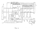
- the data processing apparatus includes an optional board slot circuit 7, a CPU 8, an address bus controller 9, a data bus controller 10 and a system controller 11, as shown in Figure 4.
- the CPU 8 is arranged to supply a status signal to an input terminal a of the optional board slot circuit 7.
- the CPU 8 and the address bus controller 9 are connected to one another by way of a local address bus, from which a high speed address bus leads to an input terminal b of the optional board slot circuit 7.
- the CPU 8 and the data bus controller 10 are connected to one another by way of a local data bus, from which a high speed data bus leads to an input terminal c of the optional board slot circuit 7.
- the system controller 11 is arranged to supply a system data DIR signal and a high speed data DIR signal, respectively, to input terminals d and e of the optional board slot circuit 7.
- the system controller 11 comprises a memory controller, and a separate line is provided between the system controller 11 and each of the address bus controller 9 and the data bus controller 10 for the purpose of synchronising the system operation. Further, a system address bus is provided between the address bus controller 9 and an input terminal g of the optional board slot circuit 7, and a system data bus is provided between the data bus controller 10 and an input terminal h of the optional board slot circuit 7. In use, a high speed signal from the CPU 8 is supplied to the address bus controller 9 and the data bus controller 10 and is latched therein by flip-flops for providing the outputs to the input terminals g and h of the optional board slot circuit 7. Accordingly, the local address and local data buses and the system address and system data buses have different time axes.
- the system of the equipment shown in Figure 3 further comprises I/O devices 12 and a CRT controller 13, which cannot be accessed at high speed and which are connected to the system address bus and the system data bus.
- An LCD controller 14 and a monitor device 15 are connected to the CRT controller 13.
- the data processing apparatus has a slot 16 for receiving an additional optional board, electrodes 16a, 16b for the supply of signals from a high speed signal line and a low speed signal line connected thereto, and a switching mechanism 17 for switching between the signal lines.
- An additional optional board 18 is to be mounted in the optional board slot 16.
- the optional board 18 may be either an optional board 18a, which uses high speed signals (and is hereinafter referred to as a high speed optional board), or a conventional optional board 18b, which uses low speed signals (and is hereinafter referred to as a low speed optional board).
- the switching mechanism 17 comprises a micro-switch 17b arranged in the vicinity of the optional board slot 16.
- a member 17a is attached to a side plane of the high speed optional board 18a such that insertion of the high speed optional board 18a into the optional board slot 16 causes the member 17a to engage and close the micro-switch 17b.
- the low speed optional board 18b has no member 17a and so the micro-switch 17b remains open when the low speed optional board 18b is inserted into the optional board slot 16.
- Figure 2 shows the configuration of the optional board slot circuit 7, incorporating the slot 16, and the micro-switch 17b.
- the signals from the system are supplied firstly to the optional board slot 16 through address bus selectors 19 and 20 and data bus selectors 21 and 22, and thence to the additional optional board 18 through the electrodes 16a and 16b of the optional board slot 16.
- the signal from the micro-switch 17b is supplied to gates of the address bus selector 19 and the data bus selector 21 by way of an inverter, to a gate of the address bus selector 20 directly, and to a gate of the data bus selector 22 by way of an OR gate.
- the OR gate receives a further input from a line 23.
- the system address bus is connected through the terminal g of the optional board slot circuit 7 to the address bus selector 19, and the high speed address bus is connected through the terminal b to the address bus selector 20.
- the CPU status signal is supplied to the address bus selector 20 from the terminal a .
- the system data bus is connected through the terminal h to the data bus selector 21, and the system data DIR signal is supplied from the terminal d to a DIR terminal of the data bus selector 21.
- the high speed data bus is connected through the terminal c to the data bus selector 22, and the high speed DIR signal is supplied from the terminal e to a DIR terminal of the data bus selector 22.
- the address bus selectors 19 and 20 may be uni-directional selectors formed from parts such as Texas Instruments 74LS244, and the data bus selectors 21 and 22 may be bi-directional selectors formed from parts such as Texas Instruments 74LS245.
- Texas Instruments part 74LS244 does not in itself function as a selector but as a uni-directional buffer. However, the selector function may be realised by the use of two parts 74LS244.
- Texas Instruments part 74LS245 does not in itself function as a bi-directional selector but rather as a buffer, the selector function being obtained by the use of two parts 74LS245.
- the micro-switch 17b remains in an open state because the low speed optional board has no member to engage the micro-switch 17b.
- a low level signal is applied to the gates of the address bus selector 19 and the data bus selector 21, and a high level signal is applied to the gates of the address bus selector 20 and the data bus selector 22.
- the address bus selector 19 and the data bus selector 21 are selected, and the system address bus and the system data bus are connected to the low speed optional board 18b.
- the member 17a engages the micro-switch 17b, so that the micro-switch 17b assumes a closed state.
- a high level signal is applied to the gates of the address bus selector 19 and the data bus selector 21, and a low level signal is applied to the gate of the address bus selector 20.
- a low level signal is also applied to the gate of the data bus selector 22 as soon as a low level signal is supplied from the line 23.
- the address bus selector 20 and the data bus selector 22 are selected, and the high speed address bus and the high speed data bus are connected to the high speed optional board 18a.
- the signal which is produced when the high speed optional board uses the high speed data bus is supplied to the line 23 to inform the system controller 11 that the high speed data bus is in use so that appropriate control is ensured and use of the high speed data bus is inhibited except where needed.
- the processing speed of the CPU is utilised to a maximum extent because the high speed address bus and the high speed data bus are directly connected to the CPU.
- the invention thus provides a compact form of data processing apparatus, which can nevertheless fulfil the requirement of supplying signals for operating either one of a conventional low speed additional optional board and a high speed additional optional board.
Landscapes
- Engineering & Computer Science (AREA)
- Theoretical Computer Science (AREA)
- General Engineering & Computer Science (AREA)
- Computer Hardware Design (AREA)
- Physics & Mathematics (AREA)
- General Physics & Mathematics (AREA)
- Power Engineering (AREA)
- Human Computer Interaction (AREA)
- Computer And Data Communications (AREA)
- Multi Processors (AREA)
- Time-Division Multiplex Systems (AREA)
Applications Claiming Priority (2)
| Application Number | Priority Date | Filing Date | Title |
|---|---|---|---|
| JP67273/89 | 1989-03-18 | ||
| JP1067273A JPH02245811A (ja) | 1989-03-18 | 1989-03-18 | 情報処理装置 |
Publications (2)
| Publication Number | Publication Date |
|---|---|
| EP0401960A2 true EP0401960A2 (fr) | 1990-12-12 |
| EP0401960A3 EP0401960A3 (fr) | 1991-06-12 |
Family
ID=13340193
Family Applications (1)
| Application Number | Title | Priority Date | Filing Date |
|---|---|---|---|
| EP19900302924 Withdrawn EP0401960A3 (fr) | 1989-03-18 | 1990-03-19 | Ordinateur avec un connecteur pour une carte d'extension |
Country Status (3)
| Country | Link |
|---|---|
| EP (1) | EP0401960A3 (fr) |
| JP (1) | JPH02245811A (fr) |
| KR (1) | KR900015002A (fr) |
Cited By (4)
| Publication number | Priority date | Publication date | Assignee | Title |
|---|---|---|---|---|
| EP0445343A1 (fr) * | 1990-03-09 | 1991-09-11 | Hsi Kuang Ma | Ordinateur portable avec des ouvertures pour introduire des batteries interchangeable et des cartes d'expansion |
| FR2671887A1 (fr) * | 1991-01-21 | 1992-07-24 | Systolic Sarl | Dispositif electronique permettant la connexion et la deconnexion d'une ligne de bus d'un systeme informatique. |
| WO1993022730A1 (fr) * | 1992-05-04 | 1993-11-11 | Compaq Computer Corporation | Circuit d'acheminement de signaux pour support d'extension de microprocesseur |
| US5473766A (en) * | 1991-09-11 | 1995-12-05 | Compaq Computer Corp. | Signal routing circuit for interchangeable microprocessor socket |
Family Cites Families (2)
| Publication number | Priority date | Publication date | Assignee | Title |
|---|---|---|---|---|
| US4314353A (en) * | 1978-03-09 | 1982-02-02 | Motorola Inc. | On chip ram interconnect to MPU bus |
| JPS59186020A (ja) * | 1983-04-07 | 1984-10-22 | Fanuc Ltd | デ−タ転送制御方式 |
-
1989
- 1989-03-18 JP JP1067273A patent/JPH02245811A/ja active Pending
-
1990
- 1990-03-19 EP EP19900302924 patent/EP0401960A3/fr not_active Withdrawn
- 1990-03-19 KR KR1019900003629A patent/KR900015002A/ko not_active Withdrawn
Cited By (4)
| Publication number | Priority date | Publication date | Assignee | Title |
|---|---|---|---|---|
| EP0445343A1 (fr) * | 1990-03-09 | 1991-09-11 | Hsi Kuang Ma | Ordinateur portable avec des ouvertures pour introduire des batteries interchangeable et des cartes d'expansion |
| FR2671887A1 (fr) * | 1991-01-21 | 1992-07-24 | Systolic Sarl | Dispositif electronique permettant la connexion et la deconnexion d'une ligne de bus d'un systeme informatique. |
| US5473766A (en) * | 1991-09-11 | 1995-12-05 | Compaq Computer Corp. | Signal routing circuit for interchangeable microprocessor socket |
| WO1993022730A1 (fr) * | 1992-05-04 | 1993-11-11 | Compaq Computer Corporation | Circuit d'acheminement de signaux pour support d'extension de microprocesseur |
Also Published As
| Publication number | Publication date |
|---|---|
| EP0401960A3 (fr) | 1991-06-12 |
| KR900015002A (ko) | 1990-10-25 |
| JPH02245811A (ja) | 1990-10-01 |
Similar Documents
| Publication | Publication Date | Title |
|---|---|---|
| EP0600410B1 (fr) | Appareil de traitement d'information du type notebook avec crayon d'entrée de données | |
| US5117225A (en) | Computer display screen monitoring system | |
| US6009492A (en) | Expansion device and computer system to which expansion device can be connected | |
| EP0597373A1 (fr) | Dispositif d'entrée de données pour un système de serrure comportant une clé active | |
| US5461222A (en) | Memory card | |
| EP1626335A2 (fr) | Dispositif d'affichage et appareil électronique portable | |
| EP0401960A2 (fr) | Ordinateur avec un connecteur pour une carte d'extension | |
| US6192437B1 (en) | Transmission apparatus with control circuit/relay within each card providing connection to related card output depending on related slot ID/ redundancy/non-redundancy, working/protection signals | |
| JPH113137A (ja) | 拡張ボード実装構造 | |
| EP0182097B1 (fr) | Adaptateur vidéo connecté en série | |
| EP0407068A2 (fr) | Terminal vidéo | |
| JP3414670B2 (ja) | 電気機器 | |
| EP0317068A2 (fr) | Système de traitement d'information avec commutation automatique d'horloge | |
| JPH0793053A (ja) | Posシステム用制御ボード | |
| CN106781106B (zh) | 用于自动存取款设备的信号接收电路及自动存取款设备 | |
| JPH06242864A (ja) | 接続方式 | |
| KR20000032319A (ko) | 액정모니터 인터페이스 장치 및 그의 전원 제어 방법 | |
| CN216067468U (zh) | 不具有主板的示教器、机器人及其系统 | |
| JP3201562B2 (ja) | 電子機器およびその制御法 | |
| KR200254175Y1 (ko) | 단말기병렬모니터링제어장치 | |
| JPH0415819A (ja) | 端末制御装置 | |
| JPH07225640A (ja) | プリント板共用化回路 | |
| KR100597743B1 (ko) | 입력장치 및 이를 사용하는 컴퓨터 시스템 | |
| JPH05208535A (ja) | プリンタ | |
| JPH06222860A (ja) | 電子回路部品の活線脱着方法 |
Legal Events
| Date | Code | Title | Description |
|---|---|---|---|
| PUAI | Public reference made under article 153(3) epc to a published international application that has entered the european phase |
Free format text: ORIGINAL CODE: 0009012 |
|
| AK | Designated contracting states |
Kind code of ref document: A2 Designated state(s): DE FR GB |
|
| PUAL | Search report despatched |
Free format text: ORIGINAL CODE: 0009013 |
|
| AK | Designated contracting states |
Kind code of ref document: A3 Designated state(s): DE FR GB |
|
| 17P | Request for examination filed |
Effective date: 19911014 |
|
| STAA | Information on the status of an ep patent application or granted ep patent |
Free format text: STATUS: THE APPLICATION HAS BEEN WITHDRAWN |
|
| 18W | Application withdrawn |
Withdrawal date: 19920228 |