EP0402671A1 - Outils avec couche abrasive de diamant de forme large ou irrégulière - Google Patents
Outils avec couche abrasive de diamant de forme large ou irrégulière Download PDFInfo
- Publication number
- EP0402671A1 EP0402671A1 EP90109870A EP90109870A EP0402671A1 EP 0402671 A1 EP0402671 A1 EP 0402671A1 EP 90109870 A EP90109870 A EP 90109870A EP 90109870 A EP90109870 A EP 90109870A EP 0402671 A1 EP0402671 A1 EP 0402671A1
- Authority
- EP
- European Patent Office
- Prior art keywords
- diamond
- tool
- substrate
- set forth
- sheet
- Prior art date
- Legal status (The legal status is an assumption and is not a legal conclusion. Google has not performed a legal analysis and makes no representation as to the accuracy of the status listed.)
- Withdrawn
Links
- 239000010432 diamond Substances 0.000 title claims abstract description 99
- 229910003460 diamond Inorganic materials 0.000 title claims abstract description 98
- 239000000758 substrate Substances 0.000 claims abstract description 45
- 238000005229 chemical vapour deposition Methods 0.000 claims abstract description 25
- 238000000034 method Methods 0.000 claims abstract description 22
- 229910045601 alloy Inorganic materials 0.000 claims description 29
- 239000000956 alloy Substances 0.000 claims description 29
- VYZAMTAEIAYCRO-UHFFFAOYSA-N Chromium Chemical group [Cr] VYZAMTAEIAYCRO-UHFFFAOYSA-N 0.000 claims description 8
- 229910052804 chromium Inorganic materials 0.000 claims description 8
- 239000011651 chromium Substances 0.000 claims description 8
- 238000005137 deposition process Methods 0.000 claims description 6
- 238000003754 machining Methods 0.000 claims description 5
- RTAQQCXQSZGOHL-UHFFFAOYSA-N Titanium Chemical compound [Ti] RTAQQCXQSZGOHL-UHFFFAOYSA-N 0.000 claims description 4
- 239000002131 composite material Substances 0.000 claims description 4
- 229910052719 titanium Inorganic materials 0.000 claims description 4
- 239000010936 titanium Substances 0.000 claims description 4
- 238000001816 cooling Methods 0.000 claims description 3
- 230000001788 irregular Effects 0.000 claims description 3
- 238000010438 heat treatment Methods 0.000 claims description 2
- 239000000463 material Substances 0.000 abstract description 10
- PXHVJJICTQNCMI-UHFFFAOYSA-N Nickel Chemical compound [Ni] PXHVJJICTQNCMI-UHFFFAOYSA-N 0.000 description 20
- 239000007789 gas Substances 0.000 description 14
- KDLHZDBZIXYQEI-UHFFFAOYSA-N Palladium Chemical compound [Pd] KDLHZDBZIXYQEI-UHFFFAOYSA-N 0.000 description 12
- 229910052759 nickel Inorganic materials 0.000 description 10
- 239000000203 mixture Substances 0.000 description 9
- 238000012360 testing method Methods 0.000 description 8
- XUIMIQQOPSSXEZ-UHFFFAOYSA-N Silicon Chemical compound [Si] XUIMIQQOPSSXEZ-UHFFFAOYSA-N 0.000 description 7
- 229910052751 metal Inorganic materials 0.000 description 7
- 239000002184 metal Substances 0.000 description 7
- ZOXJGFHDIHLPTG-UHFFFAOYSA-N Boron Chemical compound [B] ZOXJGFHDIHLPTG-UHFFFAOYSA-N 0.000 description 6
- 229910052796 boron Inorganic materials 0.000 description 6
- 238000005219 brazing Methods 0.000 description 6
- 229910052763 palladium Inorganic materials 0.000 description 6
- 229910052710 silicon Inorganic materials 0.000 description 6
- 239000010703 silicon Substances 0.000 description 6
- 239000010941 cobalt Substances 0.000 description 5
- 229910017052 cobalt Inorganic materials 0.000 description 5
- GUTLYIVDDKVIGB-UHFFFAOYSA-N cobalt atom Chemical compound [Co] GUTLYIVDDKVIGB-UHFFFAOYSA-N 0.000 description 5
- 230000008018 melting Effects 0.000 description 5
- 238000002844 melting Methods 0.000 description 5
- XEEYBQQBJWHFJM-UHFFFAOYSA-N Iron Chemical compound [Fe] XEEYBQQBJWHFJM-UHFFFAOYSA-N 0.000 description 4
- 238000005520 cutting process Methods 0.000 description 4
- UONOETXJSWQNOL-UHFFFAOYSA-N tungsten carbide Chemical compound [W+]#[C-] UONOETXJSWQNOL-UHFFFAOYSA-N 0.000 description 4
- 229910052799 carbon Inorganic materials 0.000 description 3
- 238000004519 manufacturing process Methods 0.000 description 3
- 150000002739 metals Chemical class 0.000 description 3
- 230000000717 retained effect Effects 0.000 description 3
- WFKWXMTUELFFGS-UHFFFAOYSA-N tungsten Chemical compound [W] WFKWXMTUELFFGS-UHFFFAOYSA-N 0.000 description 3
- OKTJSMMVPCPJKN-UHFFFAOYSA-N Carbon Chemical compound [C] OKTJSMMVPCPJKN-UHFFFAOYSA-N 0.000 description 2
- RYGMFSIKBFXOCR-UHFFFAOYSA-N Copper Chemical compound [Cu] RYGMFSIKBFXOCR-UHFFFAOYSA-N 0.000 description 2
- UFHFLCQGNIYNRP-UHFFFAOYSA-N Hydrogen Chemical compound [H][H] UFHFLCQGNIYNRP-UHFFFAOYSA-N 0.000 description 2
- ZOKXTWBITQBERF-UHFFFAOYSA-N Molybdenum Chemical compound [Mo] ZOKXTWBITQBERF-UHFFFAOYSA-N 0.000 description 2
- 230000015556 catabolic process Effects 0.000 description 2
- 239000000919 ceramic Substances 0.000 description 2
- 238000006243 chemical reaction Methods 0.000 description 2
- 229910052802 copper Inorganic materials 0.000 description 2
- 239000010949 copper Substances 0.000 description 2
- 238000006731 degradation reaction Methods 0.000 description 2
- 230000032798 delamination Effects 0.000 description 2
- PCHJSUWPFVWCPO-UHFFFAOYSA-N gold Chemical compound [Au] PCHJSUWPFVWCPO-UHFFFAOYSA-N 0.000 description 2
- 229910052737 gold Inorganic materials 0.000 description 2
- 239000010931 gold Substances 0.000 description 2
- 229910052739 hydrogen Inorganic materials 0.000 description 2
- 239000001257 hydrogen Substances 0.000 description 2
- 229910052742 iron Inorganic materials 0.000 description 2
- VNWKTOKETHGBQD-UHFFFAOYSA-N methane Chemical compound C VNWKTOKETHGBQD-UHFFFAOYSA-N 0.000 description 2
- 229910052750 molybdenum Inorganic materials 0.000 description 2
- 239000011733 molybdenum Substances 0.000 description 2
- 229910021334 nickel silicide Inorganic materials 0.000 description 2
- RUFLMLWJRZAWLJ-UHFFFAOYSA-N nickel silicide Chemical compound [Ni]=[Si]=[Ni] RUFLMLWJRZAWLJ-UHFFFAOYSA-N 0.000 description 2
- 230000006911 nucleation Effects 0.000 description 2
- 238000010899 nucleation Methods 0.000 description 2
- 239000002245 particle Substances 0.000 description 2
- 239000010453 quartz Substances 0.000 description 2
- 229910010271 silicon carbide Inorganic materials 0.000 description 2
- HBMJWWWQQXIZIP-UHFFFAOYSA-N silicon carbide Chemical compound [Si+]#[C-] HBMJWWWQQXIZIP-UHFFFAOYSA-N 0.000 description 2
- VYPSYNLAJGMNEJ-UHFFFAOYSA-N silicon dioxide Inorganic materials O=[Si]=O VYPSYNLAJGMNEJ-UHFFFAOYSA-N 0.000 description 2
- 229910052709 silver Inorganic materials 0.000 description 2
- 239000004332 silver Substances 0.000 description 2
- 238000007740 vapor deposition Methods 0.000 description 2
- 239000004215 Carbon black (E152) Substances 0.000 description 1
- PWHULOQIROXLJO-UHFFFAOYSA-N Manganese Chemical compound [Mn] PWHULOQIROXLJO-UHFFFAOYSA-N 0.000 description 1
- 229910039444 MoC Inorganic materials 0.000 description 1
- BQCADISMDOOEFD-UHFFFAOYSA-N Silver Chemical compound [Ag] BQCADISMDOOEFD-UHFFFAOYSA-N 0.000 description 1
- QCWXUUIWCKQGHC-UHFFFAOYSA-N Zirconium Chemical compound [Zr] QCWXUUIWCKQGHC-UHFFFAOYSA-N 0.000 description 1
- 239000002253 acid Substances 0.000 description 1
- 229910052782 aluminium Inorganic materials 0.000 description 1
- XAGFODPZIPBFFR-UHFFFAOYSA-N aluminium Chemical compound [Al] XAGFODPZIPBFFR-UHFFFAOYSA-N 0.000 description 1
- 238000013459 approach Methods 0.000 description 1
- 238000003776 cleavage reaction Methods 0.000 description 1
- 230000000295 complement effect Effects 0.000 description 1
- 239000000470 constituent Substances 0.000 description 1
- 238000011109 contamination Methods 0.000 description 1
- 239000013078 crystal Substances 0.000 description 1
- 238000001514 detection method Methods 0.000 description 1
- 238000006073 displacement reaction Methods 0.000 description 1
- 230000007613 environmental effect Effects 0.000 description 1
- 238000002474 experimental method Methods 0.000 description 1
- 239000011888 foil Substances 0.000 description 1
- 229910052735 hafnium Inorganic materials 0.000 description 1
- VBJZVLUMGGDVMO-UHFFFAOYSA-N hafnium atom Chemical compound [Hf] VBJZVLUMGGDVMO-UHFFFAOYSA-N 0.000 description 1
- 229930195733 hydrocarbon Natural products 0.000 description 1
- 150000002430 hydrocarbons Chemical class 0.000 description 1
- 238000010884 ion-beam technique Methods 0.000 description 1
- 239000007788 liquid Substances 0.000 description 1
- 229910052748 manganese Inorganic materials 0.000 description 1
- 239000011572 manganese Substances 0.000 description 1
- WPBNNNQJVZRUHP-UHFFFAOYSA-L manganese(2+);methyl n-[[2-(methoxycarbonylcarbamothioylamino)phenyl]carbamothioyl]carbamate;n-[2-(sulfidocarbothioylamino)ethyl]carbamodithioate Chemical compound [Mn+2].[S-]C(=S)NCCNC([S-])=S.COC(=O)NC(=S)NC1=CC=CC=C1NC(=S)NC(=O)OC WPBNNNQJVZRUHP-UHFFFAOYSA-L 0.000 description 1
- 239000011159 matrix material Substances 0.000 description 1
- 239000000155 melt Substances 0.000 description 1
- NFFIWVVINABMKP-UHFFFAOYSA-N methylidynetantalum Chemical compound [Ta]#C NFFIWVVINABMKP-UHFFFAOYSA-N 0.000 description 1
- 238000012986 modification Methods 0.000 description 1
- 230000004048 modification Effects 0.000 description 1
- MGRWKWACZDFZJT-UHFFFAOYSA-N molybdenum tungsten Chemical compound [Mo].[W] MGRWKWACZDFZJT-UHFFFAOYSA-N 0.000 description 1
- 229910052758 niobium Inorganic materials 0.000 description 1
- 239000010955 niobium Substances 0.000 description 1
- GUCVJGMIXFAOAE-UHFFFAOYSA-N niobium atom Chemical compound [Nb] GUCVJGMIXFAOAE-UHFFFAOYSA-N 0.000 description 1
- 238000005498 polishing Methods 0.000 description 1
- 238000010791 quenching Methods 0.000 description 1
- 239000003870 refractory metal Substances 0.000 description 1
- 230000007017 scission Effects 0.000 description 1
- 229910003468 tantalcarbide Inorganic materials 0.000 description 1
- 229910052715 tantalum Inorganic materials 0.000 description 1
- GUVRBAGPIYLISA-UHFFFAOYSA-N tantalum atom Chemical compound [Ta] GUVRBAGPIYLISA-UHFFFAOYSA-N 0.000 description 1
- 238000012546 transfer Methods 0.000 description 1
- 238000002834 transmittance Methods 0.000 description 1
- MTPVUVINMAGMJL-UHFFFAOYSA-N trimethyl(1,1,2,2,2-pentafluoroethyl)silane Chemical compound C[Si](C)(C)C(F)(F)C(F)(F)F MTPVUVINMAGMJL-UHFFFAOYSA-N 0.000 description 1
- 229910052721 tungsten Inorganic materials 0.000 description 1
- 239000010937 tungsten Substances 0.000 description 1
- 229910052720 vanadium Inorganic materials 0.000 description 1
- LEONUFNNVUYDNQ-UHFFFAOYSA-N vanadium atom Chemical compound [V] LEONUFNNVUYDNQ-UHFFFAOYSA-N 0.000 description 1
- 230000000007 visual effect Effects 0.000 description 1
- 229910052726 zirconium Inorganic materials 0.000 description 1
Images

Classifications
-
- C—CHEMISTRY; METALLURGY
- C23—COATING METALLIC MATERIAL; COATING MATERIAL WITH METALLIC MATERIAL; CHEMICAL SURFACE TREATMENT; DIFFUSION TREATMENT OF METALLIC MATERIAL; COATING BY VACUUM EVAPORATION, BY SPUTTERING, BY ION IMPLANTATION OR BY CHEMICAL VAPOUR DEPOSITION, IN GENERAL; INHIBITING CORROSION OF METALLIC MATERIAL OR INCRUSTATION IN GENERAL
- C23C—COATING METALLIC MATERIAL; COATING MATERIAL WITH METALLIC MATERIAL; SURFACE TREATMENT OF METALLIC MATERIAL BY DIFFUSION INTO THE SURFACE, BY CHEMICAL CONVERSION OR SUBSTITUTION; COATING BY VACUUM EVAPORATION, BY SPUTTERING, BY ION IMPLANTATION OR BY CHEMICAL VAPOUR DEPOSITION, IN GENERAL
- C23C16/00—Chemical coating by decomposition of gaseous compounds, without leaving reaction products of surface material in the coating, i.e. chemical vapour deposition [CVD] processes
- C23C16/22—Chemical coating by decomposition of gaseous compounds, without leaving reaction products of surface material in the coating, i.e. chemical vapour deposition [CVD] processes characterised by the deposition of inorganic material, other than metallic material
- C23C16/26—Deposition of carbon only
- C23C16/27—Diamond only
- C23C16/271—Diamond only using hot filaments
-
- B—PERFORMING OPERATIONS; TRANSPORTING
- B24—GRINDING; POLISHING
- B24D—TOOLS FOR GRINDING, BUFFING OR SHARPENING
- B24D3/00—Physical features of abrasive bodies, or sheets, e.g. abrasive surfaces of special nature; Abrasive bodies or sheets characterised by their constituents
- B24D3/02—Physical features of abrasive bodies, or sheets, e.g. abrasive surfaces of special nature; Abrasive bodies or sheets characterised by their constituents the constituent being used as bonding agent
- B24D3/04—Physical features of abrasive bodies, or sheets, e.g. abrasive surfaces of special nature; Abrasive bodies or sheets characterised by their constituents the constituent being used as bonding agent and being essentially inorganic
- B24D3/06—Physical features of abrasive bodies, or sheets, e.g. abrasive surfaces of special nature; Abrasive bodies or sheets characterised by their constituents the constituent being used as bonding agent and being essentially inorganic metallic or mixture of metals with ceramic materials, e.g. hard metals, "cermets", cements
- B24D3/10—Physical features of abrasive bodies, or sheets, e.g. abrasive surfaces of special nature; Abrasive bodies or sheets characterised by their constituents the constituent being used as bonding agent and being essentially inorganic metallic or mixture of metals with ceramic materials, e.g. hard metals, "cermets", cements for porous or cellular structure, e.g. for use with diamonds as abrasives
-
- C—CHEMISTRY; METALLURGY
- C30—CRYSTAL GROWTH
- C30B—SINGLE-CRYSTAL GROWTH; UNIDIRECTIONAL SOLIDIFICATION OF EUTECTIC MATERIAL OR UNIDIRECTIONAL DEMIXING OF EUTECTOID MATERIAL; REFINING BY ZONE-MELTING OF MATERIAL; PRODUCTION OF A HOMOGENEOUS POLYCRYSTALLINE MATERIAL WITH DEFINED STRUCTURE; SINGLE CRYSTALS OR HOMOGENEOUS POLYCRYSTALLINE MATERIAL WITH DEFINED STRUCTURE; AFTER-TREATMENT OF SINGLE CRYSTALS OR A HOMOGENEOUS POLYCRYSTALLINE MATERIAL WITH DEFINED STRUCTURE; APPARATUS THEREFOR
- C30B25/00—Single-crystal growth by chemical reaction of reactive gases, e.g. chemical vapour-deposition growth
- C30B25/02—Epitaxial-layer growth
-
- C—CHEMISTRY; METALLURGY
- C30—CRYSTAL GROWTH
- C30B—SINGLE-CRYSTAL GROWTH; UNIDIRECTIONAL SOLIDIFICATION OF EUTECTIC MATERIAL OR UNIDIRECTIONAL DEMIXING OF EUTECTOID MATERIAL; REFINING BY ZONE-MELTING OF MATERIAL; PRODUCTION OF A HOMOGENEOUS POLYCRYSTALLINE MATERIAL WITH DEFINED STRUCTURE; SINGLE CRYSTALS OR HOMOGENEOUS POLYCRYSTALLINE MATERIAL WITH DEFINED STRUCTURE; AFTER-TREATMENT OF SINGLE CRYSTALS OR A HOMOGENEOUS POLYCRYSTALLINE MATERIAL WITH DEFINED STRUCTURE; APPARATUS THEREFOR
- C30B29/00—Single crystals or homogeneous polycrystalline material with defined structure characterised by the material or by their shape
- C30B29/02—Elements
- C30B29/04—Diamond
Definitions
- the present invention generally relates to tools having a diamond abrasive layer brazed to a substrate. More particularly, the present invention relates to such tools wherein the diamond abrasive layer is fully dense polycrystalline diamond of at least about 0.1 mm thickness manufactured by a chemical vapor deposition (CVD) process.
- CVD chemical vapor deposition
- Polycrystalline diamond compacts comprising a diamond layer bonded directly to a larger cemented carbide support mass are well known in the art, for example, as described in U. S. Patent Re. 32,380. While such polycrystalline compacts represent a significant contribution to the art in many fields of use, thermal degradation at an elevated temperature, e.g., above about 700 o C, did limit their usefulness, especially in metal matrix bond applications.
- European Patent Publication No. 116,403 describes a thermally stable diamond compact comprising a mass of diamond particles present in an amount of from 80 to 90 volume percent of the body and a second phase present in an amount of 10 to 20 volume percent of the body, said second phase containing nickel and silicon, the nickel being in the form of nickel and/or nickel silicide and the silicon being in the form of silicon, silicon carbide and/or nickel silicide.
- British patent application no. 8508295 describes a thermally stable diamond compact comprising a mass of diamond particles present in an amount of from 80 to 90 volume percent of the compact and a second phase present in an amount of from 10 to 20 volume percent of the compact, said second phase containing silicon either as silicon metal or as silicon carbide.
- thermally stable diamond compacts As can be appreciated from the foregoing, extensive efforts have been made to provide thermally stable diamond compacts. However, diamond, whether synthetic or natural, is very difficult to wet, making attachment of diamond to a variety of substrates very difficult. Slutz, et al. in U. S. Patent Application Serial No. 158,575, filed February 22, 1988, and assigned to the same assignee as the present invention, discovered that thermally stable polycrystalline diamond compacts such as the foregoing can be more effectively brazed to a cemented carbide support using a chromium-containing braze alloy having a liquidus above about 700 o C.
- European Patent Application No. 254,560 discloses CVD diamond films of from less than 10 microns thickness to more than 200 microns thickness which were deposited directly onto a substrate.
- CVD diamond films of from less than 10 microns thickness to more than 200 microns thickness which were deposited directly onto a substrate.
- Example 7 suggests that the bond between the diamond film and the substrate is very weak when the diamond film is thick since no cutting test results are provided for the films having a thickness of 80, 160 and 220 microns.
- European Patent Application No. 286,306 also discloses thick (i.e., greater than about 0.1 mm thickness) CVD diamond films, but again there is no teaching that such thick films can be effectively utilized in abrasive or cutting applications; see page 12, lines 45 -47.
- Still another object of the present invention is to provide a method for making tools, especially those having a large and/or irregularly shaped fully dense diamond layer brazed to a substrate.
- the large and/or irregularly shaped diamond sheet has a length of at least about 30 millimeters, and most preferably at least about 50 millimeters in its longest dimension and has a thickness of at least about 0.1 millimeters.
- the substrate be a cemented carbide and that the braze alloy contain a carbide-former, with chromium and titanium being the most preferred of such carbide-formers.
- Tools of the present invention can be prepared by a process which comprises the steps of:
- the present invention provides tools comprising a fully dense, thermally stable diamond sheet manufactured by a low pressure deposition process which is brazed to a suitable substrate.
- Large and/or irregularly shaped diamond tools are unique to the present invention.
- such tools have a longest dimension of at least about 30 mm, and most preferably at least about 50 mm, and employ a diamond layer having a thickness of at least about 0.1 mm, and preferably between 0.1 mm and 1.0 mm.
- any low pressure deposition process for example, chemical vapor deposition, for making diamond can be utilized to make the diamond sheets which are brazed to the substrate.
- low pressure deposition process is meant any process wherein carbon is deposited on a surface to form diamond or diamond-like material in a manner similar to CVD processes.
- diamond and diamond-like films prepared by ionization vapor deposition and ion beam vapor deposition are within the intended scope of the invention.
- apparatus 10 comprises a hollow cylindrical reaction chamber 11, of a high temperature resistant material such as quartz, with opposite closed end walls 12 and 13. Positioned coaxially in chamber 11 in spaced apart, planar, and opposite parallel relationship is a pair of rectangular substrate plates or panels 14 and 15. Panels 14 and 15 are suspended in parallel relationship at a predetermined fixed spacing from each other so that a gas entering chamber 11 through gas inlet 16 in closed end 12 may flow between plates 14 and 15 to exit from chamber 11 through gas exit aperture 17 in closed end 13. Between plates 14 and 15, parallel therewith, and spaced equidistantly therefrom is an electrical resistance heater in the form of a small diameter straight tungsten wire filament 18.
- an electrical resistance heater in the form of a small diameter straight tungsten wire filament 18.
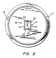
- Heater filament 18 is connected by means of electrical leads 19 and 20 to a source of direct current electrical power. Filament 18 is retained in predetermined spaced relationship from substrate panels 14 and 15 coextensively along the length of panels 14 and 15. Panels 14 and 15 may be maintained in the parallel, fixed, spaced apart relationship as shown by being joined in a subassembly which is placed in chamber 11. Such a subassembly is more clearly illustrated in FIG. 2 as subassembly 22.
- subassenbly 22 comprises a pair of rectangular panels 14 and 15 placed in planar juxtaposed position and retained in spaced apart parallel relationship by means of a short, small diameter quartz tube section 23 positioned at each corner of one panel such as panel 14 to extend perpendicularly from the plane of the panel to engage a complementary corner of the opposite panel 15 in perpendicular relationship.
- a small aperture is provided at each panel corner in axial alignment with the tube section 23.
- a short length of small diameter metal wire 24 such as tungsten wire is inserted through one aperture in one panel to extend through the tube section 23 and project from the opposite aperture in the opposite panel.
- the ends of wire 24 are bent over to retain the wire in the tube sections 23 and to fasten panels 14 and 15 to the tube sections while at the same time to fasten the tube sections to the panels.
- the length of tube sections 23 fixes the spaced apart dimension of the panels 14 and 15 in subassembly 22.
- Subassembly 22 with its plural substrate panels 14 and 15 may be conveniently hung from small J hook supports 25 as illustrated in FIG. 1.
- a predetermined gas mixture for example, a hydrogen/hydrocarbon gas mixture is caused to flow into chamber 11 through gas inlet 16 in closed end 12 and to flow unimpeded between panels or plates 14 and 15 along and in contact with heater 18, and to exit from chamber 11 through a gas exit 17 in closed end 13.
- Heater 18 is provided with sufficient electrical current to cause it to become incandescent. Under these conditions the flow of gas cones into contact with and is activated by incandescent heater 18. The gas flow also comes into contact with panels 14 and 15 which are cooler than heater 18 to cause diamond crystal nucleation and growth on panels 14 and 15, particularly on those opposite surfaces directly exposed to heater filament 18.
- Panels 14 and 15 serve as plural substrate surfaces in CVD apparatus 10, and both are served by one or more heater filaments 18.
- Panels 14 and 15 contain or are manufactured from those materials which are conducive to diamond nucleation and growth in a CVD process.
- the preferred materials are metals which are stable at high temperatures and in the presence of a high carbon content gas.
- the refractory metals represent a class of metals useful for panels 14 and 15, and molybdenum has been used with good results.
- heater filament 18 During operation, heater filament 18 remains at its incandescent temperature subject to some temperature variations brought on by environmental conditions such as minor equipment variations and the like. Temperature variations, particularly during start up from room temperature, cause the heater filament 18 to be subjected to temperature and chemically induced stresses causing flexing and embrittlement of the filament 18 with resultant changes in the spacing between the heater filament and plates 14 and 15. For best results, heater filament 18 should be maintained in a fixed space relationship to panels 14 and 15. For example, a spacing of less than about 1 cm has been found to provide good results.
- heater filament 18 Since heater filament 18 is maintained at its incandescent temperature, its intrinsic strength is significantly reduced and attachment of devices intending to maintain the described spaced relationship tend to cause filament breakage and a short useful life. As a consequence, in one embodiment of this invention a very precise force and leverage means in the form of a weight balancing assembly is utilized to maintain the spaced distance of heater filament 18 constant along the length of panels 14 and 15.
- a weight balancing system employed in the present invention is illustrated in FIG. 1 as weight balancing assembly 26.
- heater filament 18 is maintained above about 2000°C.
- a gas mixture of about 95-99% by volume hydrogen and about 1-5% by volume methane is introduced into reaction chamber 11 to cause a gas flow therein of from about 0.5 cc/min. to about 3 cc/min.
- Operating parameters of gas mixture constituents and proportions, gas flow rate, and electrical power input to heater 18 are retained constant for the appropriate period of time, with the result that panels 14 and 15 become coated with a diamond layer of from about 0.1 mm to 1.0 mm or more in thickness.
- This diamond layer typically mechanically delaminates from substrate panels 14 and 15 during cooling as integral, cohesive, self-supporting diamond sheets or strips.
- the resultant diamond sheets are typically polycrystalline and very highly wear resistant with no significant cleavage planes or soft wear directions. Such diamond sheets are thermally stable and can be heated to high temperature brazing conditions without damage.
- such CVD diamond sheets are cut, for example, with a laser, or machined by means well known in the art, to a size and shape which is roughly equivalent to that of the substrate to which it is to be brazed.
- the thus prepared diamond layer is then placed on top of a sheet of a suitable braze alloy which in turn has been placed on top of a suitable substrate having nearly the desired shape and dimensions of the finished tool.
- Such arrangement is then heated in a furnace maintained at a temperature above the melting point of the braze alloy for a time sufficient to at least partly melt the braze alloy and thereby cause the diamond sheet to strongly adhere to the substrate.
- furnace brazing Such a process is known in the art as furnace brazing. It should be understood, however, that tools of the present invention can be manufactured by methods other than furnace brazing, for example, according to the methods disclosed in U. S. Patent No. 4,225,322 to Knemeyer.
- the braze alloy contain a carbide-former, with chromium being the most preferred of such carbide-formers.
- carbide-forming elements which can be utilized in the preferred braze alloys include, for example, manganese, titanium, tungsten, hafnium, zirconium, vanadium, molybdenum, niobium, and tantalum.
- the braze alloy should have a liquidus above 700 o C but less than 1200 o C, at which temperature thermal degradation of the diamond may commence.
- Representative metals for inclusion in the braze alloy composition include, for example, nickel, cobalt, gold, boron, palladium, silver, copper and the like.
- braze alloys are described in the patent literature.
- One such braze alloy is disclosed in U.S. Patent No. 4,149,881 as consisting essentially of from about 17 to 44 percent by weight of palladium, from about 4 to about 11 percent by weight of chromium, from about 1 to about 4 percent by weight of silicon, from about 1.5 to about 4 percent by weight boron, with the balance being nickel.
- braze alloy is described in U. S. Patent No. 4,396,577 as consisting essentially of 25 to 95 percent by weight of palladium, up to 5 percent by weight of silicon, up to 3.5 percent by weight of boron, and the remainder being cobalt.
- U. S. Patent No. 4,414,178 discloses a braze alloy consisting essentially of 28 to 32 percent by weight of palladium, about 6 to 13 percent by weight of chromium, about 1. to 3.5 percent by weight boron, and the balance being nickel, which is particularly suited for use in the present invention.
- Still another braze alloy suitable for use in the present invention is disclosed in U. S. Patent No. 4,772,294, and which consists essentially of 20 to 80 percent by weight of palladium, 2 to 13 percent by weight of chromium, 1 to 4 percent by weight of boron, and the remainder being nickel.
- brazing alloy patents are hereby incorporated by reference into the present disclosure.
- suitable materials can readily be ascertained by those skilled in the art without undue experimentation.
- the substrate may be any suitable material and is typically a cemented carbide such as cemented tungsten carbide, cemented titanium carbide, cemented tungsten-molybdenum carbide, or cemented tantalum carbide.
- the metal bond material for the carbide is generally selected from the group consisting of cobalt, nickel, iron and mixtures thereof. Cobalt is the bond material of choice in the art as is the use of a cobalt cemented tungsten carbide substrate.
- the most preferred alternative to a cemented carbide substrate is a ceramic substrate such as SIALON.
- tools of the present invention may have several layers of diamond. Such embodiments would be particularly useful for chip control in machining operations or depth of cut control in drill bits.
- Tools manufactured in accordance with the present invention can be used for any application in which prior art tools were used. Such tools may be made of a single element or of a mosiac arrangement.
- the bonding apparatus consisted of a RF heater with the coil around an air-actuated carbide plunger which compresses the diamond layer to the braze layer to the carbide substrate to the apparatus support.
- the RF coil heats the carbide plunger and the heat is transferred to the diamond layer which diffuses it to the braze layer.
- the braze melts and bonds to the diamond and carbide layers.
- This operation is accomplished in a matter of seconds and the endpoint is obtained by a combination of linear displacement of the carbide plunger relative to the system support and the visual detection of braze flow. Temperature quench was obtained by turning off the RF power at the occurrence of braze alloy melting and the end of thinning of the braze as determined by the end of braze flow.
- the resultant brazed sanples were shaped by diamond grinding and polishing operations.
- the 4.5 mm leg length sample and the 6.5 mm leg length sample were brazed into tool shanks.
- the samples were tested against a 390 aluminum workpiece under dry conditions at a surface speed of 2200 SFPM, a 0.020 inch depth of cut and a 0.005 inch ipr feed rate.
- the tools were resharpened twice to test the quality versus diamond relative to depth. Tests were run on each.
- the CVD diamond tools performed as well as to slightly better than polycrystalline diamond tools. Performance was similar after each resharpening.
- the experiment was repeated with slight modification as follows. First, the surfaces were lapped before brazing and second, the braze alloy was quenched more rapidly once it became liquid so as to prevent the alloy from seeping out of the diamond/carbide interface. This resulted in a product which did not suffer from the delamination.
- the parts were cleaned as in Example 1 and then assembled with the diamond, braze alloy and carbide or ceramic (SIALON type) substrate pressed against one another with a weight on top to ensure adequate contact.
- This assembly was placed in a vacuum furnace and heated under a vacuum of about 10-4 torr for about 1.5 hours to 900 o C, held for 15 minutes and quenched. The parts were finished without layer delamination.
- the 60 mm x 19 mm sample was further cut by wire EDM cutting the carbide substrate to the diamond layer and snapping the diamond layer along the cut.
- the diamond did not delaminate and the break followed the EDM cut in the carbide support.
Landscapes
- Chemical & Material Sciences (AREA)
- Engineering & Computer Science (AREA)
- Materials Engineering (AREA)
- Inorganic Chemistry (AREA)
- Mechanical Engineering (AREA)
- Metallurgy (AREA)
- Organic Chemistry (AREA)
- Crystallography & Structural Chemistry (AREA)
- Ceramic Engineering (AREA)
- General Chemical & Material Sciences (AREA)
- Chemical Kinetics & Catalysis (AREA)
- Crystals, And After-Treatments Of Crystals (AREA)
- Polishing Bodies And Polishing Tools (AREA)
- Cutting Tools, Boring Holders, And Turrets (AREA)
- Ceramic Products (AREA)
Applications Claiming Priority (2)
| Application Number | Priority Date | Filing Date | Title |
|---|---|---|---|
| US36682389A | 1989-06-15 | 1989-06-15 | |
| US366823 | 1999-08-04 |
Publications (1)
| Publication Number | Publication Date |
|---|---|
| EP0402671A1 true EP0402671A1 (fr) | 1990-12-19 |
Family
ID=23444699
Family Applications (1)
| Application Number | Title | Priority Date | Filing Date |
|---|---|---|---|
| EP90109870A Withdrawn EP0402671A1 (fr) | 1989-06-15 | 1990-05-23 | Outils avec couche abrasive de diamant de forme large ou irrégulière |
Country Status (6)
| Country | Link |
|---|---|
| EP (1) | EP0402671A1 (fr) |
| JP (1) | JPH0369568A (fr) |
| KR (1) | KR910000303A (fr) |
| CA (1) | CA2012821A1 (fr) |
| IE (1) | IE901296A1 (fr) |
| ZA (1) | ZA901817B (fr) |
Cited By (7)
| Publication number | Priority date | Publication date | Assignee | Title |
|---|---|---|---|---|
| EP0459807A1 (fr) * | 1990-05-30 | 1991-12-04 | Semiconductor Energy Laboratory Co., Ltd. | Revêtement de diamant à usage industriel et méthode pour son obtention |
| EP0492160A1 (fr) * | 1990-12-20 | 1992-07-01 | General Electric Company | Produits symmétriques en diamant et procédé de leur production |
| US5366579A (en) * | 1990-03-26 | 1994-11-22 | Semiconductor Energy Laboratory Co., Ltd. | Industrial diamond coating and method of manufacturing |
| US5500248A (en) * | 1994-08-04 | 1996-03-19 | General Electric Company | Fabrication of air brazable diamond tool |
| US5529805A (en) * | 1994-09-22 | 1996-06-25 | General Electric Company | Method for manufacturing a diamond article |
| US5626909A (en) * | 1994-12-07 | 1997-05-06 | General Electric Company | Fabrication of brazable in air tool inserts |
| US7261753B2 (en) * | 2002-07-26 | 2007-08-28 | Mitsubishi Materials Corporation | Bonding structure and bonding method for cemented carbide element and diamond element, cutting tip and cutting element for drilling tool, and drilling tool |
Families Citing this family (2)
| Publication number | Priority date | Publication date | Assignee | Title |
|---|---|---|---|---|
| JP2008006507A (ja) * | 2006-06-26 | 2008-01-17 | Ebara Corp | ダイヤモンド研磨工具、ダイヤモンド研磨工具の作成方法、ダイヤモンド研磨工具の再生方法 |
| CN119501477B (zh) * | 2024-10-12 | 2026-05-01 | 中国航发贵州黎阳航空动力有限公司 | 一种航空发动机钛合金异形件的加工方法 |
Citations (9)
| Publication number | Priority date | Publication date | Assignee | Title |
|---|---|---|---|---|
| US4224380A (en) * | 1978-03-28 | 1980-09-23 | General Electric Company | Temperature resistant abrasive compact and method for making same |
| US4247305A (en) * | 1979-07-27 | 1981-01-27 | General Electric Company | Abrasive structures and methods of their preparation |
| FR2512430A1 (fr) * | 1981-09-04 | 1983-03-11 | Sumitomo Electric Industries | Agglomere de diamant pour outil et procede de fabrication de cet agglomere |
| US4380471A (en) * | 1981-01-05 | 1983-04-19 | General Electric Company | Polycrystalline diamond and cemented carbide substrate and synthesizing process therefor |
| US4403015A (en) * | 1979-10-06 | 1983-09-06 | Sumitomo Electric Industries, Ltd. | Compound sintered compact for use in a tool and the method for producing the same |
| EP0116403A1 (fr) * | 1983-01-10 | 1984-08-22 | De Beers Industrial Diamond Division (Proprietary) Limited | Produit abrasif |
| US4707384A (en) * | 1984-06-27 | 1987-11-17 | Santrade Limited | Method for making a composite body coated with one or more layers of inorganic materials including CVD diamond |
| EP0254560A1 (fr) * | 1986-07-23 | 1988-01-27 | Sumitomo Electric Industries Limited | Diamant fabriqué en phase gazeuse et son procédé de production |
| US4734339A (en) * | 1984-06-27 | 1988-03-29 | Santrade Limited | Body with superhard coating |
-
1990
- 1990-03-08 ZA ZA901817A patent/ZA901817B/xx unknown
- 1990-03-22 CA CA002012821A patent/CA2012821A1/fr not_active Abandoned
- 1990-04-10 IE IE129690A patent/IE901296A1/en unknown
- 1990-05-23 EP EP90109870A patent/EP0402671A1/fr not_active Withdrawn
- 1990-06-12 JP JP2151763A patent/JPH0369568A/ja active Pending
- 1990-06-14 KR KR1019900008733A patent/KR910000303A/ko not_active Withdrawn
Patent Citations (9)
| Publication number | Priority date | Publication date | Assignee | Title |
|---|---|---|---|---|
| US4224380A (en) * | 1978-03-28 | 1980-09-23 | General Electric Company | Temperature resistant abrasive compact and method for making same |
| US4247305A (en) * | 1979-07-27 | 1981-01-27 | General Electric Company | Abrasive structures and methods of their preparation |
| US4403015A (en) * | 1979-10-06 | 1983-09-06 | Sumitomo Electric Industries, Ltd. | Compound sintered compact for use in a tool and the method for producing the same |
| US4380471A (en) * | 1981-01-05 | 1983-04-19 | General Electric Company | Polycrystalline diamond and cemented carbide substrate and synthesizing process therefor |
| FR2512430A1 (fr) * | 1981-09-04 | 1983-03-11 | Sumitomo Electric Industries | Agglomere de diamant pour outil et procede de fabrication de cet agglomere |
| EP0116403A1 (fr) * | 1983-01-10 | 1984-08-22 | De Beers Industrial Diamond Division (Proprietary) Limited | Produit abrasif |
| US4707384A (en) * | 1984-06-27 | 1987-11-17 | Santrade Limited | Method for making a composite body coated with one or more layers of inorganic materials including CVD diamond |
| US4734339A (en) * | 1984-06-27 | 1988-03-29 | Santrade Limited | Body with superhard coating |
| EP0254560A1 (fr) * | 1986-07-23 | 1988-01-27 | Sumitomo Electric Industries Limited | Diamant fabriqué en phase gazeuse et son procédé de production |
Cited By (13)
| Publication number | Priority date | Publication date | Assignee | Title |
|---|---|---|---|---|
| US5366579A (en) * | 1990-03-26 | 1994-11-22 | Semiconductor Energy Laboratory Co., Ltd. | Industrial diamond coating and method of manufacturing |
| US5254141A (en) * | 1990-05-30 | 1993-10-19 | Semiconductor Energy Laboratory Co., Ltd. | Industrial diamond coating and method of manufacturing the same |
| EP0459807A1 (fr) * | 1990-05-30 | 1991-12-04 | Semiconductor Energy Laboratory Co., Ltd. | Revêtement de diamant à usage industriel et méthode pour son obtention |
| EP0492160A1 (fr) * | 1990-12-20 | 1992-07-01 | General Electric Company | Produits symmétriques en diamant et procédé de leur production |
| US5647878A (en) * | 1994-08-04 | 1997-07-15 | General Electric Company | Fabrication of brazable in air diamond tool inserts and inserts fabricated thereby |
| US5500248A (en) * | 1994-08-04 | 1996-03-19 | General Electric Company | Fabrication of air brazable diamond tool |
| US5529805A (en) * | 1994-09-22 | 1996-06-25 | General Electric Company | Method for manufacturing a diamond article |
| US5626909A (en) * | 1994-12-07 | 1997-05-06 | General Electric Company | Fabrication of brazable in air tool inserts |
| US7261753B2 (en) * | 2002-07-26 | 2007-08-28 | Mitsubishi Materials Corporation | Bonding structure and bonding method for cemented carbide element and diamond element, cutting tip and cutting element for drilling tool, and drilling tool |
| CN100358670C (zh) * | 2002-07-26 | 2008-01-02 | 三菱麻铁里亚尔株式会社 | 硬质合金和金刚石件的熔合结构和方法及钻具与其切削件 |
| US7621974B2 (en) * | 2002-07-26 | 2009-11-24 | Mitsubishi Materials Corporation | Bonding structure and bonding method for cemented carbide element and diamond element, cutting tip and cutting element for drilling tool, and drilling tool |
| US8147573B2 (en) | 2002-07-26 | 2012-04-03 | Mitsubishi Materials Corporation | Bonding structure and bonding method for cemented carbide element and diamond element, cutting tip and cutting element for drilling tool, and drilling tool |
| US8728184B2 (en) | 2002-07-26 | 2014-05-20 | Mitsubishi Materials Corporation | Bonding structure and bonding method for cemented carbide element and diamond element, cutting tip and cutting element for drilling tool, and drilling tool |
Also Published As
| Publication number | Publication date |
|---|---|
| JPH0369568A (ja) | 1991-03-25 |
| CA2012821A1 (fr) | 1990-12-15 |
| IE901296L (en) | 1990-12-15 |
| ZA901817B (en) | 1991-04-24 |
| KR910000303A (ko) | 1991-01-29 |
| IE901296A1 (en) | 1991-01-02 |
Similar Documents
| Publication | Publication Date | Title |
|---|---|---|
| US4239502A (en) | Diamond and cubic boron nitride grinding wheels with improved silver alloy bonds | |
| EP0694510B1 (fr) | Braser d'un film de diamant à carbure de tungstène | |
| US4670025A (en) | Thermally stable diamond compacts | |
| AU611210B2 (en) | Brazed thermally-stable polycrystalline diamond compact workpieces and their fabrication | |
| US5529805A (en) | Method for manufacturing a diamond article | |
| US5264071A (en) | Free standing diamond sheet and method and apparatus for making same | |
| US5647878A (en) | Fabrication of brazable in air diamond tool inserts and inserts fabricated thereby | |
| US4931363A (en) | Brazed thermally-stable polycrystalline diamond compact workpieces | |
| EP0329955A2 (fr) | Fixation d'arêtes tranchantes thermostables sur des outils en carbides | |
| KR100210900B1 (ko) | 본딩 공구 | |
| US4496372A (en) | Abrasive bodies | |
| EP0101259A1 (fr) | Corps abrasifs | |
| EP0104063B1 (fr) | Corps abrasifs comprenant du nitrure de bore | |
| EP0116403B1 (fr) | Produit abrasif | |
| CN103687829A (zh) | 钎焊的涂布的含金刚石材料 | |
| IE921793A1 (en) | Chemically bonded adherent coating for abrasive compacts and¹method for making same | |
| IE901296A1 (en) | Tools Employing A Large Or Irregularly Shaped Diamond¹Abrasive Layer | |
| JP2012525274A (ja) | 物品の取り付け方法又は物品の取り付けを改善する方法 | |
| CA1086509A (fr) | Diamants et nitrure de bore cubique reunis a un support metallique par un alliage d'ag-mn-zr | |
| GB2163144A (en) | Thermally stable diamond compacts | |
| EP3129182B1 (fr) | Assemblage brase de superabrasif avec un joint de brasage de métal actif ayant une couche de relaxation des contraintes ; methode de fabrication d'un tel assemblage | |
| JPH07228962A (ja) | 硬質層被覆部材 | |
| EP0206652A2 (fr) | Méthode de fabrication d'une ébauche d'un foret | |
| JPH07196379A (ja) | 気相合成ダイヤモンドろう付け工具およびその製造方法 | |
| EP0706850B1 (fr) | Compacts de nitrure de bore cubique contenant du cobalt, aptes au brasage |
Legal Events
| Date | Code | Title | Description |
|---|---|---|---|
| PUAI | Public reference made under article 153(3) epc to a published international application that has entered the european phase |
Free format text: ORIGINAL CODE: 0009012 |
|
| AK | Designated contracting states |
Kind code of ref document: A1 Designated state(s): AT BE CH DE FR GB LI SE |
|
| 17P | Request for examination filed |
Effective date: 19910523 |
|
| 17Q | First examination report despatched |
Effective date: 19921104 |
|
| STAA | Information on the status of an ep patent application or granted ep patent |
Free format text: STATUS: THE APPLICATION IS DEEMED TO BE WITHDRAWN |
|
| 18D | Application deemed to be withdrawn |
Effective date: 19941201 |