EP0403174B1 - Circuit amplificateur différentiel à grande vitesse de fonctionnement - Google Patents
Circuit amplificateur différentiel à grande vitesse de fonctionnement Download PDFInfo
- Publication number
- EP0403174B1 EP0403174B1 EP90306261A EP90306261A EP0403174B1 EP 0403174 B1 EP0403174 B1 EP 0403174B1 EP 90306261 A EP90306261 A EP 90306261A EP 90306261 A EP90306261 A EP 90306261A EP 0403174 B1 EP0403174 B1 EP 0403174B1
- Authority
- EP
- European Patent Office
- Prior art keywords
- fet
- source
- voltage
- fets
- drain
- Prior art date
- Legal status (The legal status is an assumption and is not a legal conclusion. Google has not performed a legal analysis and makes no representation as to the accuracy of the status listed.)
- Expired - Lifetime
Links
- 230000005669 field effect Effects 0.000 claims description 3
- 238000010586 diagram Methods 0.000 description 6
- 230000035945 sensitivity Effects 0.000 description 3
- JBRZTFJDHDCESZ-UHFFFAOYSA-N AsGa Chemical compound [As]#[Ga] JBRZTFJDHDCESZ-UHFFFAOYSA-N 0.000 description 2
- 229910001218 Gallium arsenide Inorganic materials 0.000 description 2
- 238000010276 construction Methods 0.000 description 2
- 230000001737 promoting effect Effects 0.000 description 2
- 239000004065 semiconductor Substances 0.000 description 2
- 230000033228 biological regulation Effects 0.000 description 1
- 150000001875 compounds Chemical class 0.000 description 1
- 230000007423 decrease Effects 0.000 description 1
- 230000006866 deterioration Effects 0.000 description 1
- 230000000694 effects Effects 0.000 description 1
- 238000004088 simulation Methods 0.000 description 1
- 239000000758 substrate Substances 0.000 description 1
- 230000001131 transforming effect Effects 0.000 description 1
Images




Classifications
-
- H—ELECTRICITY
- H03—ELECTRONIC CIRCUITRY
- H03F—AMPLIFIERS
- H03F3/00—Amplifiers with only discharge tubes or only semiconductor devices as amplifying elements
- H03F3/45—Differential amplifiers
- H03F3/45071—Differential amplifiers with semiconductor devices only
- H03F3/45076—Differential amplifiers with semiconductor devices only characterised by the way of implementation of the active amplifying circuit in the differential amplifier
- H03F3/45376—Differential amplifiers with semiconductor devices only characterised by the way of implementation of the active amplifying circuit in the differential amplifier using junction FET transistors as the active amplifying circuit
- H03F3/45381—Long tailed pairs
- H03F3/45385—Non-folded cascode stages
-
- H—ELECTRICITY
- H03—ELECTRONIC CIRCUITRY
- H03F—AMPLIFIERS
- H03F2203/00—Indexing scheme relating to amplifiers with only discharge tubes or only semiconductor devices as amplifying elements covered by H03F3/00
- H03F2203/45—Indexing scheme relating to differential amplifiers
- H03F2203/45024—Indexing scheme relating to differential amplifiers the differential amplifier amplifying transistors are cascode coupled transistors
-
- H—ELECTRICITY
- H03—ELECTRONIC CIRCUITRY
- H03F—AMPLIFIERS
- H03F2203/00—Indexing scheme relating to amplifiers with only discharge tubes or only semiconductor devices as amplifying elements covered by H03F3/00
- H03F2203/45—Indexing scheme relating to differential amplifiers
- H03F2203/45186—Indexing scheme relating to differential amplifiers the differential amplifier contains clamping components in the load circuit
-
- H—ELECTRICITY
- H03—ELECTRONIC CIRCUITRY
- H03F—AMPLIFIERS
- H03F2203/00—Indexing scheme relating to amplifiers with only discharge tubes or only semiconductor devices as amplifying elements covered by H03F3/00
- H03F2203/45—Indexing scheme relating to differential amplifiers
- H03F2203/45244—Indexing scheme relating to differential amplifiers the differential amplifier contains one or more explicit bias circuits, e.g. to bias the tail current sources, to bias the load transistors
-
- H—ELECTRICITY
- H03—ELECTRONIC CIRCUITRY
- H03F—AMPLIFIERS
- H03F2203/00—Indexing scheme relating to amplifiers with only discharge tubes or only semiconductor devices as amplifying elements covered by H03F3/00
- H03F2203/45—Indexing scheme relating to differential amplifiers
- H03F2203/45641—Indexing scheme relating to differential amplifiers the LC being controlled, e.g. by a signal derived from a non specified place in the dif amp circuit
Definitions
- the present invention relates to a differential amplifying circuit of the type using field effect transistors (FETs) and applicable to semiconductor integrated circuits or similar circuitry. More particularly, the present invention is concerned with a differential amplifying FET circuit with a common source connection circuit formed on a compound semiconductor (for example, gallium arsenide) substrate.
- FETs field effect transistors
- a differential amplifying circuit as described above has been proposed in various forms in the past. To better understand the present invention, a brief reference will be made to some prior art differential amplifying circuits.
- FIG. 1 shows a prior art differential amplifying circuit with input terminals 10 and 12.
- An input voltage VI and a reference voltage VR1 are applied to the input terminals 10 and 12, respectively.
- a differential input section 14 is connected to the input terminals 10 and 12 and has a pair of enhancement type FETs 16 and 18.
- the FET 16 is turned on and off by the input voltage VI, while the FET 18 is turned on and off by the reference voltage VR1.
- the FETS 16 and 18 have drains connected to a load section 20, and sources connected to a negative power source voltage VSS via an enhancement type FET 22. This FET 22 plays the role of a constant current source.
- the load section 20 has a depletion type FET 24 connected between a positive power source voltage VDD and the drain of the FET 16, and a depletion type FET 26 connected between the power source voltage VDD and the drain of the FET 18.
- the FETs 24 and 26 serve as load elements.
- Output terminals 28 and 30 on which output voltages outl and out2 appear, respectively, are connected to the drains of the FETs 16 and 1 8, respectively.
- the reference numeral 32 designates an input terminal assigned to a reference voltage VR2.
- the prior art differential amplifying circuit having the above construction uses the FETs 24 and 26 as load elements and selects a saturation drain current of such elements which is substantially one half the current of the constant current source 22.
- a drawback with this configuration is that when the input voltage VI having a great amplitude arrives, the resultant output waveform appears stepwise and is thereby degraded.
- FIG. 2 shows another prior art differential amplifying circuit which is disclosed in JP-B-89007522.
- the same components are designated by like reference numerals, and redundant description will be avoided for simplicity.
- the circuit of FIG. 2 is distinguishable over the circuit of FIG. 1 in that depletion type FETs 40 and 42 are provided in place of the load FETs 24 and 26, and that Zener diodes 44 and 46 are respectively connected in parallel with the FETs 40 and 42 in opposite direction.
- the reference numerals 47 and 48 designate input terminals assigned to input voltages VI1 and VI2, respectively.
- a differential amplifier circuit which comprises a first input port for receiving an input voltage; a first field effect transistor having a drain, a source and a gate which is responsive to said input voltage to control conduction between said drain and said source; a second FET having a drain, a source and a gate which is responsive to a first reference voltage to control conduction between said drain and said source of said second FET, said source of said second FET being connected to said source of said first FET; a constant current source connected to said sources of said first and second FETs for supplying a constant current from said sources of said first and second FETs to a low potential power source; a third FET having a drain connected to a high potential power source and having a source connected to a first output port to act as a
- a differential amplifying circuit as defined above with reference to an IEEE conference paper, is characterized in that said third FET has a gate connected to said first node which is connected to said drain of said first FET and said fourth FET has a gate connected to said second node which is connected to said drain of said second FET.
- the third and fourth FETs each is implemented as a depletion type FET.
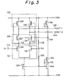
- FIG. 3 shows a differential amplifying circuit embodying the present invention.
- the circuit has an input terminal 110 to which an input voltage VI is applied, and a differential input section 112 connected to the input terminal 110.
- the differential input section 112 is made up of enhancement type FETs 114 and 116.
- the enhancement type FET 114 is connected to the input terminal 110, while the enhancement type FET 116 is connected to a node N1 on which a first reference voltage VR1 appears.
- Resistors 118 and 120 are connected between the node NI and a high potential power source VDD and between the node NI and a low potential power source VSS, respectively.
- the drains of the FETs 114 and 116 are connected at nodes N2 and N3, respectively, to a load section 122 and a switch section 124.
- the sources of the FETs 114 and 116 are connected to the low potential power source VSS via an enhancement type FET 126 which plays the role of a constant current source.
- the load section 122 has a depletion type FET 128 which is connected to the node N2 at the gate thereof, and a depletion type FET/30 connected to the node N3 at the gate thereof.
- the FETs 128 and 130 serve as load elements.
- the source voltage VDD is connected to the drains of the FETs 128 and 130, while the switch section 124 is connected to the sources of the FETs 128 and 130.
- the switch section 124 has an enhancement type FET 132 whose drain is connected to the source of the FET 128, and an enhancement type FET 134 whose drain is connected to the source of the FET 130.
- the gates of the FETs 132 and 134 are connected commonly to a node N4 which is held at a second reference voltage VR2.
- a depletion type FET 136 adapted for a load is connected between the node N4 and the power source voltage VDD.
- the drain of the FET 132 is connected to an output terminal 138 assigned to an output voltage OUTl, while the drain of the FET 134 is connected to an output terminal 140 assigned to an output voltage OUT2.
- a depletion type FET 142 and an enhancement type FET 144 generate a constant voltage.
- the FET or constant current source 126 causes a constant current to flow at all times between the drain and the source thereof on the basis of the constant voltage which is generated by the FETs 142 and 144 as mentioned above.
- the gate of the FET 126 is connected to the gates of the FETs 142 and 144 which are in turn connected to a node N5.
- the FETs 142 and 144 are connected in series between the node N4 and the power source voltage VSS via the node N5.
- the differential input section 112 serves the function of a circuit for controlling the FETs 114 and 116 on and off by detecting a difference between the reference voltage VR1 and the input voltage VI.
- the FETs 132 and 134 perform switching operations on the basis of the reference voltage VR2 so as to change the state of current flow sharply, whereby the logical levels of the output terminals 138 and 140 are reproduced surely and rapidly.
- the FET 128 since the gate voltage of the FET 128 is equal to the voltage on the node N2, the FET 128 is turned off when the voltage on the node N2 decreases beyond a predetermined value. Then, a current which does not exceed the capacity of the FET 126 flows into the amplifying circuit via the output terminal 138 because the FETs 114 and 132 have been turned on.
- the current coming in via the output terminal 138 turns off the FET 116 and thereby increases the voltage on the node N3.
- the FET 124 is turned off with the result that the output voltage OUT2 is turned from the low level to the high level, as shown in FIG. 4.
- the gate voltage of the FET 130 is equal to the voltage appearing on the node N3, the FET 130 turns off at the instant when the voltage on the node N3 rises above a predetermined value.
- the FETs 116 and 134 are in their OFF state, the current flows out to a succeeding circuit, not shown, via the output terminal 140 within the range which the FET 130 accommodates.
- the FET 114 On the turn of the input voltage VI from a high level to a low level, the FET 114 is turned off to in turn increase the voltage appearing on the node N2.
- the FET 132 When the voltage on the node N2 increases nearly to the second reference voltage VR2, the FET 132 is turned off and, therefore, the output voltage OUT1 is caused into a high level, as shown in FIG. 4. Since the gate voltage of the FET 128 is equal to the voltage on the node N2, the FET 128 is turned on when the voltage on the node N2 increases beyond a predetermined value. At this time, the FETs 114 and 132 are in their OFF state, so that the current flows out to the succeeding circuit via the output terminal 138 within the range determined by the capacity of the FET 128.
- the FET 116 On the outflow of the current as stated above, the FET 116 is turned on to lower the voltage on the node N3.
- the FET 134 is turned on to cause the output voltage OU2 into a low level, as shown in FIG. 4. Since the gate voltage of the FET 130 is equal to the voltage appearing on the node N3, the FET 130 is turned off when the voltage on the node N3 drops beyond a predetermined value. At this moment, the FETs 116 and 134 remain turned off and, hence, a current flows into the amplifying circuit via the output terminal 140 within the range determined by the drive capacity of the FET 126.
- FIG. 5 is a graph comparing the operation of the illustrative embodiment with that of the prior art circuitry of FIG. 1. Specifically, the curves shown in FIG. 5 simulate the relationship between the current and output voltage on the output terminal and the time, on the assumption that the constant current sources of the circuits shown in FIGS. 1 and 3 are the same, and that the load acting on the output terminal is 0.3 picofarad.
- curves labeled X and Y are associated with the circuits of FIGS. 3 and 1, respectively.
- the operation X of the illustrative embodiment achieves greater incoming and outgoing currents than the operation Y of the prior art, because the FETs 128, 130, 132 and 134 turn on and off. Such incoming and outgoing currents allow the output voltage level to settle rapidly.
- an arrangement may be made such that the first reference voltage VR1 coincides with the center of the levels of the input voltage VI, and the second reference voltage VR2 coincides with the center of the logical amplitude levels which are determined by the current ratio in the conductive state of the FETs 114, 116, 128, 130 and 126. Then, the on-off operations of the FETs 128, 130, 132 and 134 serve to set cause the logical levels of the nodes N2 and N3 or those of the output terminals 138 and 140 to settle more rapidly. This is successful in further promoting high-speed operations and in increasing the sensitivity.
- the conduction of the FET 128 is controlled by the voltage appearing on the node N2, while the conduction of the FET 130 is controlled by the voltage appearing on the node N3.
- the FETs 128 and 130 serving as load elements are implemented as depletion type FETs the ON resistance of which is comparatively small, a great current can be fed to the succeeding circuit and, yet, the power consumption is reduced.
- FIG. 6 an alternative embodiment of the differential amplifying circuit in accordance with the present invention is shown.
- the same components as those shown in FIG. 3 are designated by like reference numerals, and redundant description will be avoided for simplicity.
- the circuit of FIG. 6 differs from the circuit of FIG. 3 in that the resistors 118 and 120 for generating the first reference voltage VR1 are omitted, and that an input voltage VI ⁇ opposite in phase to the input voltage VI coming in from the outside is applied to the gate of the FET 116. Specifically, the input voltage VI ⁇ is applied to a second input terminal 146.
- the alternative embodiment is essentially the same as the previous embodiment.
- FIG. 7 is a diagram showing an input circuit which is a specific application of the illustrative embodiments state above with reference to FIGS. 3 and 6.
- the same components are designated by like reference numerals, and redundant description will be avoided for simplicity.
- the input circuit has an input terminal 150 to which an input voltage VI is applied, and an output terminal 152.
- a differential amplifying circuit 154, a level shifting circuit 156, a differential amplifying circuit 158, and a level shifting circuit 160 are cascaded in this order between the input terminal 150 and the output terminal 152.
- the differential amplifying circuits 154 and 158 are implemented by the illustrative embodiments shown in FIGS. 3 and 6, respectively.
- the level shifting circuit 156 is made up of a series connection of normally OFF FETs 156a and 156b intervening between power source voltages VDD and VSS, and a series connection of normally OFF FETs 156c and 156d also intervening between the power source voltages VDD and VSS.
- the level shifting circuit 156 has a function of lowering the voltage to below the input voltage VI.
- the gates of the FETs 156a and 156c are respectively connected to the output voltages OUT1 and OUT2 of the differential amplifying circuit 154.
- the gates of the FETs 156b and 156d are connected to the gate of the FET 144 of the differential amplifier 154.
- the output voltage between the FETs 156a and 156b and the output voltage between the FETs 156c and 156d are connected to the differential amplifier 158, while the output voltage of the differential amplifier 158 is in turn connected to the level shifting circuit 160.
- the level shifting circuit 160 has an enhancement type FET 160a, a diode 160b for shifting the level, and a depletion type FET 160c adapted for a load.
- the FET 160a, diode 160b and FET 160c are connected in series between the power source voltages VDD and VSS. Also connected in series between the power source voltages VDD and VSS are a depletion type FET 160d, a diode 160e, and an enhancement type FET 160f.
- the level shifting circuit 160 is connected to the output terminal 152 between the diode 160e and the enhancement type FET 160f.
- the input circuit shown in FIG. 7 is implemented as an input level transforming circuit, and that it is used to transform a voltage level width from the ECL level (0.3 volt in peak-to-peak value) to the DCFL level (0.6 volt in peak-to-peak value) using gallium arsenide.
- a differential amplifying circuit in accordance with the present invention has a fifth switching FET connected between the first switching FET and the third load FET, and a sixth switching FET connected between the second switching FET and the fourth load FET.
- the fifth and sixth FETs are turned on and off to change the amount of current flow sharply, so that the logical levels of various nodes settle within a short period of time and, in addition, the sensitivity is enhanced.
- the conduction of the third FET and that of the fourth FET are controlled by voltages appearing on first and second nodes, respectively. Hence, even when a circuit having a great load capacitance is connected to the output side and requires a great current, a sufficient current is insured up to the limit which depends on the drive capacity of the load FETs and the supply capacity of a constant current source. This is successful in promoting rapid operations.
- the third and fourth FETs as depletion type FETs whose ON resistance is relatively small, it is possible to feed a great current to a succeeding circuit while achieving a power saving effect.
- the enhancement type FETs 114, 116, 132 and 134 of the illustrative embodiments may be replaced with depletion type FETs.
- the enhancement type FETs 114 and 116 are replaced with depletion type FETs, it is necessary to lower the reference voltage VR1 to a level at which the FETs 114 and 116 are operable.
- the enhancement type FET 126 serving as a constant current source may be replaced with a FET whose gate and source are short-circuited or even with a resistor.
Landscapes
- Engineering & Computer Science (AREA)
- Power Engineering (AREA)
- Logic Circuits (AREA)
- Amplifiers (AREA)
Claims (6)
- Circuit amplificateur différentiel comprenant:un premier accès d'entrée pour recevoir une tension d'entrée;un premier transistor à effet de champ (TEF) (114) ayant un drain, une source et une grille qui est sensible à ladite tension d'entrée (VI) pour commander la conduction entre ledit drain et ladite source;un deuxième TEF (116) ayant un drain, une source et une grille qui est sensible à une première tension de référence (VRI) pour commander la conduction entre ledit drain et ladite source dudit deuxième TEF (116), ladite source dudit deuxième TEF (116) étant connectée à ladite source dudit premier TEF (114);une source (126) de courant constant connectée auxdites sources desdits premier et deuxième TEF (114, 116) pour fournir un courant constant desdites sources desdits premier et deuxième TEF (114, 116) à une source de puissance (VSS) à potentiel bas;un troisième TEF (128) ayant un drain connecté à une source (VDD) de puissance à potentiel élevé et ayant une source connectée à un premier accès de sortie (OUT1) pour jouer le rôle de charge;un quatrième TEF (130) ayant un drain connecté à ladite source de puissance à potentiel élevé (VDD) et ayant une source connectée à une deuxième sortie (OUT2) pour jouer le rôle de charge;un cinquième TEF (132) ayant un drain connecté à ladite source dudit troisième TEF (128) et une source connectée à un premier noeud (N2), ledit cinquième TEF (132) ayant une grille qui est sensible à une deuxième tension de référence (VR2) pour commander la conduction entre ledit drain et ladite source dudit cinquième TEF (132); etun sixième TEF (134) ayant un drain connecté à ladite source dudit quatrième TEF (130) et ayant une source connectée à un deuxième noeud (N3), ledit sixième TEF (134) ayant une grille qui est connectée à ladite grille dudit cinquième TEF (132) et qui est sensible à ladite deuxième tension de référence (VR2) pour commander la conduction entre ledit drain et ladite source dudit sixième TEF (134), ladite deuxième tension de référence (VR2) étant indépendante de la conduction desdits premier à sixième TEF (114, 116, 128, 130, 132, 134), caractérisé en ce que ledit troisième TEF (128) a une grille connectée à un premier noeud (N2) qui est connecté audit drain dudit premier TEF (114) et en ce que ledit quatrième TEF (130) a une grille connectée à un deuxième noeud (N3) qui est connecté audit drain dudit deuxième TEF (116).
- Circuit selon la revendication 1, comprenant en outre un deuxième accès d'entrée connecté à ladite grille dudit deuxième TEF (116) pour recevoir une tension (V1) qui est en opposition de phase par rapport à ladite tension d'entrée (V1) afin de fournir à ladite grille dudit deuxième TEF (116) une première tension de référence (VR1).
- Circuit selon la revendication 1 ou 2, dans lequel lesdits troisième et quatrième TEF (128, 130) comprennent chacun un TEF du type à déplétion.
- Circuit selon la revendication 1, 2 ou 3, dans lequel lesdits premier, deuxième, cinquième et sixième TEF (114, 116, 132, 134) comprennent chacun un TEF du type à enrichissement.
- Circuit selon la revendication 1, 2 ou 3, dans lequel lesdits premier, deuxième, cinquième et sixième TEF (114, 116, 132, 134) comprennent chacun un TEF du type à déplétion.
- Circuit selon l'une quelconque des revendications précédentes, dans lequel ladite source (126) de courant constant comprend un TEF du type à enrichissement.
Applications Claiming Priority (2)
| Application Number | Priority Date | Filing Date | Title |
|---|---|---|---|
| JP148749/89 | 1989-06-12 | ||
| JP1148749A JP2544808B2 (ja) | 1989-06-12 | 1989-06-12 | 差動増幅回路 |
Publications (3)
| Publication Number | Publication Date |
|---|---|
| EP0403174A2 EP0403174A2 (fr) | 1990-12-19 |
| EP0403174A3 EP0403174A3 (fr) | 1991-07-03 |
| EP0403174B1 true EP0403174B1 (fr) | 1996-04-24 |
Family
ID=15459770
Family Applications (1)
| Application Number | Title | Priority Date | Filing Date |
|---|---|---|---|
| EP90306261A Expired - Lifetime EP0403174B1 (fr) | 1989-06-12 | 1990-06-08 | Circuit amplificateur différentiel à grande vitesse de fonctionnement |
Country Status (4)
| Country | Link |
|---|---|
| US (1) | US5065111A (fr) |
| EP (1) | EP0403174B1 (fr) |
| JP (1) | JP2544808B2 (fr) |
| DE (1) | DE69026648T2 (fr) |
Families Citing this family (9)
| Publication number | Priority date | Publication date | Assignee | Title |
|---|---|---|---|---|
| US6320429B1 (en) | 1991-06-28 | 2001-11-20 | Fuji Electric Co., Ltd. | Integrated circuit having a comparator circuit including at least one differential amplifier |
| JPH0514073A (ja) * | 1991-06-28 | 1993-01-22 | Fuji Electric Co Ltd | 差動増幅器及び比較器 |
| JP3516307B2 (ja) * | 1992-12-24 | 2004-04-05 | ヒュンダイ エレクトロニクス アメリカ | デジタルトランジスタで構成される差動アナログトランジスタ |
| US5514902A (en) * | 1993-09-16 | 1996-05-07 | Mitsubishi Denki Kabushiki Kaisha | Semiconductor device having MOS transistor |
| JP3609260B2 (ja) * | 1998-07-17 | 2005-01-12 | 沖電気工業株式会社 | 半導体装置の増幅回路 |
| US6377121B1 (en) * | 2000-09-29 | 2002-04-23 | Intel Corporation | Dynamic cascoding technique for operational amplifiers |
| JP2002124835A (ja) * | 2000-10-13 | 2002-04-26 | Seiko Epson Corp | 演算増幅回路、定電圧回路および基準電圧回路 |
| JP4054804B2 (ja) * | 2002-04-23 | 2008-03-05 | ナノパワーソリューション株式会社 | 雑音除去回路 |
| JP4582705B2 (ja) * | 2005-03-17 | 2010-11-17 | 株式会社リコー | ボルテージレギュレータ回路 |
Family Cites Families (4)
| Publication number | Priority date | Publication date | Assignee | Title |
|---|---|---|---|---|
| FR1395336A (fr) * | 1964-05-13 | 1965-04-09 | Const Radio Electr Et Electron | Amplificateur symétrique de puissance à liaison directe |
| JPS59100626A (ja) * | 1982-11-30 | 1984-06-09 | Fujitsu Ltd | 電流切り換え型論理回路 |
| US4533877A (en) * | 1983-12-29 | 1985-08-06 | At&T Bell Laboratories | Telecommunication operational amplifier |
| JPS647522A (en) * | 1987-06-30 | 1989-01-11 | Oki Electric Ind Co Ltd | X-ray mask and manufacture thereof |
-
1989
- 1989-06-12 JP JP1148749A patent/JP2544808B2/ja not_active Expired - Fee Related
-
1990
- 1990-06-08 DE DE69026648T patent/DE69026648T2/de not_active Expired - Fee Related
- 1990-06-08 EP EP90306261A patent/EP0403174B1/fr not_active Expired - Lifetime
- 1990-06-08 US US07/535,029 patent/US5065111A/en not_active Expired - Lifetime
Also Published As
| Publication number | Publication date |
|---|---|
| US5065111A (en) | 1991-11-12 |
| JP2544808B2 (ja) | 1996-10-16 |
| EP0403174A3 (fr) | 1991-07-03 |
| DE69026648T2 (de) | 1996-12-19 |
| EP0403174A2 (fr) | 1990-12-19 |
| DE69026648D1 (de) | 1996-05-30 |
| JPH0313120A (ja) | 1991-01-22 |
Similar Documents
| Publication | Publication Date | Title |
|---|---|---|
| KR920001634B1 (ko) | 중간전위 발생회로 | |
| US6885234B2 (en) | Resistance load source follower circuit | |
| EP0594305B1 (fr) | Circuit comparateur | |
| US5469085A (en) | Source follower using two pairs of NMOS and PMOS transistors | |
| JPH08195631A (ja) | センス増幅器 | |
| US6586995B1 (en) | Amplifier | |
| US5128556A (en) | Current-switching type logic circuit | |
| US5065111A (en) | Differential amplifying circuit operable at high speed | |
| EP0427557B1 (fr) | Un circuit amplificateur | |
| US4336503A (en) | Driver circuit having reduced cross-over distortion | |
| US5479116A (en) | Level conversion circuits for converting a digital input signal varying between first and second voltage levels to a digital output signal varying between first and third voltage levels | |
| US5864245A (en) | Output circuit with overvoltage protection | |
| US6236195B1 (en) | Voltage variation correction circuit | |
| US4937474A (en) | Low power, high noise margin logic gates employing enhancement mode switching FETs | |
| US4743957A (en) | Logic integrated circuit device formed on compound semiconductor substrate | |
| EP0529545B1 (fr) | Circuits intégrés CMOS pour décalage de niveau | |
| US5134319A (en) | Bicmos differential amplifier having improved switching speed | |
| JPS625725A (ja) | スイツチング電界効果トランジスタの制御ゲ−トに論理信号を加える論理回路 | |
| US6175277B1 (en) | Bias network for CMOS power devices | |
| JP3967248B2 (ja) | レベルシフト回路 | |
| US5173622A (en) | Source coupled logic circuit with reduced power consumption | |
| US5004938A (en) | MOS analog NOR amplifier and current source therefor | |
| US6459332B2 (en) | Digitally-operated analog buffer amplifiers | |
| JP3192049B2 (ja) | バッファ回路 | |
| JP2545712B2 (ja) | ガリウム砒素半導体集積回路 |
Legal Events
| Date | Code | Title | Description |
|---|---|---|---|
| PUAI | Public reference made under article 153(3) epc to a published international application that has entered the european phase |
Free format text: ORIGINAL CODE: 0009012 |
|
| AK | Designated contracting states |
Kind code of ref document: A2 Designated state(s): DE FR GB |
|
| PUAL | Search report despatched |
Free format text: ORIGINAL CODE: 0009013 |
|
| AK | Designated contracting states |
Kind code of ref document: A3 Designated state(s): DE FR GB |
|
| 17P | Request for examination filed |
Effective date: 19911121 |
|
| 17Q | First examination report despatched |
Effective date: 19940209 |
|
| GRAH | Despatch of communication of intention to grant a patent |
Free format text: ORIGINAL CODE: EPIDOS IGRA |
|
| GRAA | (expected) grant |
Free format text: ORIGINAL CODE: 0009210 |
|
| AK | Designated contracting states |
Kind code of ref document: B1 Designated state(s): DE FR GB |
|
| REF | Corresponds to: |
Ref document number: 69026648 Country of ref document: DE Date of ref document: 19960530 |
|
| ET | Fr: translation filed | ||
| PLBE | No opposition filed within time limit |
Free format text: ORIGINAL CODE: 0009261 |
|
| STAA | Information on the status of an ep patent application or granted ep patent |
Free format text: STATUS: NO OPPOSITION FILED WITHIN TIME LIMIT |
|
| 26N | No opposition filed | ||
| REG | Reference to a national code |
Ref country code: GB Ref legal event code: IF02 |
|
| PGFP | Annual fee paid to national office [announced via postgrant information from national office to epo] |
Ref country code: DE Payment date: 20060601 Year of fee payment: 17 |
|
| PGFP | Annual fee paid to national office [announced via postgrant information from national office to epo] |
Ref country code: GB Payment date: 20060607 Year of fee payment: 17 |
|
| PGFP | Annual fee paid to national office [announced via postgrant information from national office to epo] |
Ref country code: FR Payment date: 20060608 Year of fee payment: 17 |
|
| GBPC | Gb: european patent ceased through non-payment of renewal fee |
Effective date: 20070608 |
|
| REG | Reference to a national code |
Ref country code: FR Ref legal event code: ST Effective date: 20080229 |
|
| PG25 | Lapsed in a contracting state [announced via postgrant information from national office to epo] |
Ref country code: DE Free format text: LAPSE BECAUSE OF NON-PAYMENT OF DUE FEES Effective date: 20080101 |
|
| PG25 | Lapsed in a contracting state [announced via postgrant information from national office to epo] |
Ref country code: GB Free format text: LAPSE BECAUSE OF NON-PAYMENT OF DUE FEES Effective date: 20070608 |
|
| PG25 | Lapsed in a contracting state [announced via postgrant information from national office to epo] |
Ref country code: FR Free format text: LAPSE BECAUSE OF NON-PAYMENT OF DUE FEES Effective date: 20070702 |