EP0403268B1 - Gerät zur Kompensierung von Videosignalen - Google Patents
Gerät zur Kompensierung von Videosignalen Download PDFInfo
- Publication number
- EP0403268B1 EP0403268B1 EP90306463A EP90306463A EP0403268B1 EP 0403268 B1 EP0403268 B1 EP 0403268B1 EP 90306463 A EP90306463 A EP 90306463A EP 90306463 A EP90306463 A EP 90306463A EP 0403268 B1 EP0403268 B1 EP 0403268B1
- Authority
- EP
- European Patent Office
- Prior art keywords
- converter
- output
- signal
- video signal
- screen
- Prior art date
- Legal status (The legal status is an assumption and is not a legal conclusion. Google has not performed a legal analysis and makes no representation as to the accuracy of the status listed.)
- Expired - Lifetime
Links
Images









Classifications
-
- G—PHYSICS
- G09—EDUCATION; CRYPTOGRAPHY; DISPLAY; ADVERTISING; SEALS
- G09G—ARRANGEMENTS OR CIRCUITS FOR CONTROL OF INDICATING DEVICES USING STATIC MEANS TO PRESENT VARIABLE INFORMATION
- G09G3/00—Control arrangements or circuits, of interest only in connection with visual indicators other than cathode-ray tubes
- G09G3/20—Control arrangements or circuits, of interest only in connection with visual indicators other than cathode-ray tubes for presentation of an assembly of a number of characters, e.g. a page, by composing the assembly by combination of individual elements arranged in a matrix no fixed position being assigned to or needed to be assigned to the individual characters or partial characters
- G09G3/34—Control arrangements or circuits, of interest only in connection with visual indicators other than cathode-ray tubes for presentation of an assembly of a number of characters, e.g. a page, by composing the assembly by combination of individual elements arranged in a matrix no fixed position being assigned to or needed to be assigned to the individual characters or partial characters by control of light from an independent source
- G09G3/36—Control arrangements or circuits, of interest only in connection with visual indicators other than cathode-ray tubes for presentation of an assembly of a number of characters, e.g. a page, by composing the assembly by combination of individual elements arranged in a matrix no fixed position being assigned to or needed to be assigned to the individual characters or partial characters by control of light from an independent source using liquid crystals
-
- G—PHYSICS
- G09—EDUCATION; CRYPTOGRAPHY; DISPLAY; ADVERTISING; SEALS
- G09G—ARRANGEMENTS OR CIRCUITS FOR CONTROL OF INDICATING DEVICES USING STATIC MEANS TO PRESENT VARIABLE INFORMATION
- G09G2310/00—Command of the display device
- G09G2310/02—Addressing, scanning or driving the display screen or processing steps related thereto
- G09G2310/0202—Addressing of scan or signal lines
- G09G2310/0221—Addressing of scan or signal lines with use of split matrices
-
- G—PHYSICS
- G09—EDUCATION; CRYPTOGRAPHY; DISPLAY; ADVERTISING; SEALS
- G09G—ARRANGEMENTS OR CIRCUITS FOR CONTROL OF INDICATING DEVICES USING STATIC MEANS TO PRESENT VARIABLE INFORMATION
- G09G2320/00—Control of display operating conditions
- G09G2320/02—Improving the quality of display appearance
-
- G—PHYSICS
- G09—EDUCATION; CRYPTOGRAPHY; DISPLAY; ADVERTISING; SEALS
- G09G—ARRANGEMENTS OR CIRCUITS FOR CONTROL OF INDICATING DEVICES USING STATIC MEANS TO PRESENT VARIABLE INFORMATION
- G09G2320/00—Control of display operating conditions
- G09G2320/02—Improving the quality of display appearance
- G09G2320/0233—Improving the luminance or brightness uniformity across the screen
-
- G—PHYSICS
- G09—EDUCATION; CRYPTOGRAPHY; DISPLAY; ADVERTISING; SEALS
- G09G—ARRANGEMENTS OR CIRCUITS FOR CONTROL OF INDICATING DEVICES USING STATIC MEANS TO PRESENT VARIABLE INFORMATION
- G09G2320/00—Control of display operating conditions
- G09G2320/02—Improving the quality of display appearance
- G09G2320/0271—Adjustment of the gradation levels within the range of the gradation scale, e.g. by redistribution or clipping
- G09G2320/0276—Adjustment of the gradation levels within the range of the gradation scale, e.g. by redistribution or clipping for the purpose of adaptation to the characteristics of a display device, i.e. gamma correction
-
- G—PHYSICS
- G09—EDUCATION; CRYPTOGRAPHY; DISPLAY; ADVERTISING; SEALS
- G09G—ARRANGEMENTS OR CIRCUITS FOR CONTROL OF INDICATING DEVICES USING STATIC MEANS TO PRESENT VARIABLE INFORMATION
- G09G2320/00—Control of display operating conditions
- G09G2320/02—Improving the quality of display appearance
- G09G2320/0285—Improving the quality of display appearance using tables for spatial correction of display data
-
- G—PHYSICS
- G09—EDUCATION; CRYPTOGRAPHY; DISPLAY; ADVERTISING; SEALS
- G09G—ARRANGEMENTS OR CIRCUITS FOR CONTROL OF INDICATING DEVICES USING STATIC MEANS TO PRESENT VARIABLE INFORMATION
- G09G2320/00—Control of display operating conditions
- G09G2320/04—Maintaining the quality of display appearance
- G09G2320/041—Temperature compensation
-
- G—PHYSICS
- G09—EDUCATION; CRYPTOGRAPHY; DISPLAY; ADVERTISING; SEALS
- G09G—ARRANGEMENTS OR CIRCUITS FOR CONTROL OF INDICATING DEVICES USING STATIC MEANS TO PRESENT VARIABLE INFORMATION
- G09G3/00—Control arrangements or circuits, of interest only in connection with visual indicators other than cathode-ray tubes
- G09G3/20—Control arrangements or circuits, of interest only in connection with visual indicators other than cathode-ray tubes for presentation of an assembly of a number of characters, e.g. a page, by composing the assembly by combination of individual elements arranged in a matrix no fixed position being assigned to or needed to be assigned to the individual characters or partial characters
- G09G3/34—Control arrangements or circuits, of interest only in connection with visual indicators other than cathode-ray tubes for presentation of an assembly of a number of characters, e.g. a page, by composing the assembly by combination of individual elements arranged in a matrix no fixed position being assigned to or needed to be assigned to the individual characters or partial characters by control of light from an independent source
- G09G3/36—Control arrangements or circuits, of interest only in connection with visual indicators other than cathode-ray tubes for presentation of an assembly of a number of characters, e.g. a page, by composing the assembly by combination of individual elements arranged in a matrix no fixed position being assigned to or needed to be assigned to the individual characters or partial characters by control of light from an independent source using liquid crystals
- G09G3/3611—Control of matrices with row and column drivers
Definitions
- the present invention relates to a video signal compensation apparatus for compensating the video signal inputted to the dot-matrix type display with the aim of improving display non-uniformity.
- the input voltage-intensity characteristic of the liquid crystal panel has a non-linear characteristic
- the video signal is converted to carry out compensation of the display non-uniformity.
- the compensation processings are to be carried out independently by the video signals R, G and B, respectively (e.g. Japanese Patent Publication KOKAI (Unexamined) No. 62-209418).
- European Patent Application EP-A-0303510 discloses a liquid crystal display device comprising: a group of common electrodes formed on one substrate of a pair of substrates for sandwiching a liquid crystal layer; a group of segment electrodes formed on the other substrate of the pair of substrates; wherein a multiplex driving is achieved successively by applying a common voltage waveform comprising selective voltage and non-selective voltage to the group of common electrodes and applying a segment voltage waveform comprising an ON voltage and an OFF voltage to the group of segment electrodes; and wherein at least one of the common voltage waveform and the segment voltage waveform is changed in accordance with the pattern of drawings and/or characters displayed in the liquid crystal display device.
- Such a device it is intended to provide a uniform display without any contrast cross-talk by extracting the rule of the display content quantitatively, so that the compensation corresponds to the extraction.
- a compensation based on the difference between the numbers of ON pixels in adjacent common electrodes, such a device is able to compensate for zebra cross-talk.
- the single panel color filter type display includes the following drawbacks;
- the display non-uniformity characteristics at the individual screen positions differ from one another. Accordingly, it has not been possible to perform compensations effective for the whole screen by compensating the video signal by using a look-up-table stored only 1 table data for the whole screen.
- An object of embodiments of the present invention is to perform an effective compensation to the whole screen by splitting the display screen, converting the video signal by the split region of the screen, and then displaying an image on a screen, in a dot-matrix type display.
- a display apparatus comprising a dot matrix type display panel for displaying a video signal on a pixel by pixel basis for a dot clock and horizontal and vertical synchronous signals, and a video signal compensation apparatus for compensating the video signal
- said signal compensation apparatus comprises: a dot counter for counting said dot clock and outputting a first count signal indicative of a horizontal screen position; a line counter for counting said horizontal synchronous signal and outputting a second count signal indicative of a vertical screen position; a screen split control means for producing from said first and second count signal a signal indicative of a screen split region which is one of a plurality of screen split regions in the whole screen of the dot matrix type display panel; and a correction processing means responsive to said signal outputted from said screen split control means for correcting an input video signal for each of the plurality of split regions on a video signal level versus screen brightness characteristic curve of the dot matrix type display panel in each of the plurality of screen split regions so as to correct a display non
- Fig. 1 shows a construction of the liquid crystal display device using the video signal compensation apparatus in the first embodiment of the present invention.
- the numeral 10 denotes a video signal compensation apparatus, 11 a correction processing means, 11a an A/D (Analog-Digital) converter, 11b a look-up-table memory, 11c a D/A (Digital-Analog) converter, 12 an screen split control means, 12a a horizontal split bit selection circuit, 12b a vertical split bit selection circuit, 13 a dot counter, and 14 a line counter.
- the video input signals [e.g., three basic color signals of R (red), G (green) and B (blue)] are converted into the digital signals with an A/D converter 11a and are inputted to the address (e.g., lower address) of the look-up-table memory 11b, and are subjected to correction by referring to the table.
- the corrected video signals are converted to the analog signals with a D/A converter 11c.
- the signal line driver 15 By inputting to the signal line driver 15, they drive the liquid crystal panel for every selected line by the scanning line driver 16.
- the counter output which has counted the dot clock with the dot counter 13 utilizing the horizontal synchronous signal as a count clear signal is inputted to the horizontal split bit selection circuit 12a, and after having been selected to the upper bit of the counter outputs, inputted to the upper address of the look-up-table memory 11b.
- the counter output which has counted the horizontal synchronous signal with the line counter 14 utilizing the vertical synchronous signal as a count clear signal is inputted to the vertical split bit selection circuit 12b, and after having been selected to the upper bit of the counter outputs, inputted to the address (e.g., upper address) of the look-up-table memory 11b. This makes it possible to refer to the look-up-table to the screen split region.
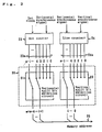
- Fig. 2 shows a construction of the screen split control means 20, which performs connections between the output line 23a of the dot counter 23, the output line 24a of the line counter 24 and the memory address line 25 of the correction processing means.
- screen splitting can be performed in 16 dot width in both horizontal and vertical directions.
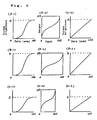
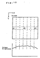
- the maximum screen brightness output indicates the levels as shown in Fig. 3 at the measured points A, B and C which denote the representative points of the screen split region, and the respective video signal level - screen brightness characteristics differ as in Fig. 4 (A-1), (B-1) and (C-1).
- the plural correction data e.g., input and output data having 8 bit width
- the video signal can be converted by using the correction data for every screen split region, so that there can be obtained an effect which makes it possible to perform a linearity correction effective for the whole screen.
- the correction data to be stored in the look-up-table memory can be the data as shown below.
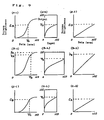
- the maximum screen brightness output indicates the level similar to that of Fig. 3 at the measuring points A, B and C which show the representative points in the screen split region and the respective video signal level - screen brightness characteristics are as in Fig. 5 (A-1), (B-1) and (C-1) . Since in this case the minimum output level in the maximum screen brightness output level by the screen split area is the value c at the measuring point C, this value c is taken as a normalization level. Assuming the plural correction data (e.g., input and output data having 8 bit width) stored in the look-up-table memory by the screen split region to be the data [shown in Fig.
- the correction data to be stored in the look-up-table memory can be the data as shown below.
- the video signal level - screen brightness characteristics at the measured points A, B and C are as in Fig. 9 (A-1), (B-1) and (C-1).
- the normalization levels by screen split area are a B , b B and c B at the measuring points A, B and C.
- screen split area e.g., input and output data having 8 bit width
- the screen split control means can be of the construction as shown below.
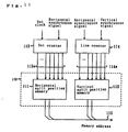
- Fig. 11 shows a construction of the screen split control means 110, which is furnished with a horizontal split position memory 111 for outputting a signal to show the horizontal split position by the count value inputted from the output line 113a of the dot counter 113 and a vertical split position memory 112 for outputting a signal to show the vertical split position by the count value inputted from the output line 114a of the line counter 114.
- the image split width can be optionally set to exercise the video signal compensation by the screen split region.
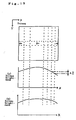
- Fig. 15 (a) as the screen split can be set by the variation ( ⁇ I) of the maximum screen brightness level, the maximum screen brightness output after the compensation conversion becomes as shown in Fig. 15 (b), by which there can be obtained such effects that the difference of brightnesss in the screen split regions decreases and the difference of color in the case of mixing the three basic colors also decreases among the screen split regions.
- screen split control means may have the construction as shown below.
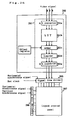
- Fig. 16 shows a construction of the screen split control means 160, which is furnished with a horizontal split position memory 161 for outputting a signal to show the horizontal split position by the count value inputted from the output line 163a of the dot counter 163, a vertical split position memory 162 for outputting a signal to show the vertical split position by the count value inputted from the output line 164a of the line counter 164, and a block address memory 166 connected to the horizontal split position memory 161 and the vertical split position memory 162 for carrying out correspondence between the screen split region and the memory address.
- the video signal compensation can be performed by the screen split region.
- the output of the horizontal split position memory 161 is 2 bits, which outputs the values of "00" - "11” as shown in Fig. 13
- the output of the vertical split position memory 162 is 2 bits, which outputs the values of "00" - "11” as shown in Fig. 14.
- the output of the block address memory 166 when it is set to 2 bit width as shown in Fig.
- the said 2 bit output is inputted as a memory address of the correction processing means. Accordingly, there can be obtained an effect that, in altering a correction data in a certain screen split region to a correction data in other screen split region, only the content of the block address memory 166 may be altered.
- the content of the block address memory 166 is very small in comparison with the correction data amount of the look-up-table memory or the like in the correction processing means, easy and high speed alteration can be realized.
- the same correction data can be used for the different screen split regions.
- the screen split regions shown by the same hatching in Fig. 18 indicate the case where the compensation conversion were carried out by using the same correction data.
- the number of the look-up-table requires only one-severalth of the number of the screen split regions (e.g., 1/4 in Fig. 18), with the result that the size of the look-up-table may be brought to one-severalth.
- the correction processing means can be of the following construction
- Fig. 19 shows a construction of the correction processing means 190, in which the video input signals (e.g., the three basic colors R, G and B) are converted to the digital signals with the A/D converter 191 and inputted to the multiplier 192, and are subjected to correction by being multiplied with the correction data from the block memory 193.
- the corrected video signal is converted to an analog signal with the D/A converter 194 and then inputted to the signal line driver.
- the video signal compensation can be carried out by using the correction data by the screen split region.
- the correction processing means an example of storing the corrected addition data by the screen split region in the block memory and converting the video signal by using an adder instead of the multiplier, an example of being provided with a voltage adder for performing addition to the video signal by means of a signal in which the output of the block memory storing the corrected addition data of the video signal by screen split region is subjected to D/A conversion, etc. can be readily analogized.
- Fig. 20 shows a construction of the liquid crystal display device using the video signal compensation apparatus in the second embodiment of the present invention.
- the numeral 200 denotes a video signal compensation apparatus, 201 a correction processing means, 201a an A/D converter, 201b a look-up-table memory, 201c a D/A converter, 201da voltage adder, 202 is a temperature control means, 202a is a temperature distribution position memory, 203 is an A/D converter, and 204 is a temperature detector.
- the video input signals (e.g., three basic color signals of R, G and B) are converted into the digital signals with an A/D converter 201a, after which they are inputted to the address (e.g., lower address) of the look-up-table memory 201b and subjected to correction by referring to the table.
- the corrected video signals are converted to the analog signals with a D/A converter 201c, after which they are further incorporated with an offset voltage by the voltage adder 241 in being added the offset voltage V AO which is in agreement with the threshold voltage which shows the rising position of the video signal level - screen brightness characteristic by the voltage adder 201d.
- the video signals are inputted to the signal line driver 205, on which they drive the liquid crystal panel 207 by the selected line by the scanning line driver 206.
- the temperature data obtained by converting the results obtained by measuring the temperature of the liquid crystal panel with the temperature detector 204 into a digital signal with the A/D converter 203 is inputted to the address (e.g., the upper address) input of the look-up-table memory 201b as its table number output after referring to the temperature distribution position memory 202a.
- the address e.g., the upper address
- the look-up-table memory 201b As its table number output after referring to the temperature distribution position memory 202a.
- the temperature is set by each case of the showing of the certain threshold voltage variation, and the table number for said temperature level is stored in the temperature distribution position memory 202a. And also, in order to prepare the correction data to be stored in the look-up-table memory 201, measurement of the video signal level - screen brightness characteristic at the said temperature level is carried out.
- the table for said variation can be arbitrarily selected, and by converting the video signal in reference to said table, there can be obtained an effect which makes it possible to perform an effective linearity compensation.
- the correction processing means can be of the following construction:
- Fig. 22 shows a construction of the correction processing means 220, in which the video input signals (e.g., the three basic colors R, G and B) are converted to the digital signals (e.g., data of 8 bits per color) with the A/D converter 221 and inputted to the address of the look-up-table memory 222, and are subjected to correction by referring to the table.
- the bit width of the output data is larger than the bit width of the input data (e.g., the output data having 9 bit width).
- the value corresponding to the temperature variation of the liquid crystal panel is subtracted by the subtractor 223, after which, in order to obtain agreement with the bit width of the input data of the look-up-table memory 222, it is subjected to limitation of the maximum value and the minimum value with the limiter 225 and converted to the analog signal by the D/A converter 226. Further, after addition of an offset voltage V AO which is in agreement with the threshold voltage which shows the rising position of the video signal level - screen brightness characteristic by the voltage adder 227, the video signals are inputted to the signal line driver.
- the subtraction amount generation memory 52d storing the data for correlating the output data from the temperature control means with the subtraction amount in the subtractor, the subtraction amount of said output is subtracted from the output data of the look-up-table memory 52e.
- the subtraction amount for the variation can be arbitrarily selected and subtracted from the compensation conversion output in the look-up-table memory, so that there can be obtained an effect which makes it possible to perform an effective linearity correction by the increase in the capacity of the look-up-table memory to only about two times.
- Fig. 24 shows a construction of the liquid crystal display device using the video signal compensation apparatus in the third embodiment of the present invention.
- the numeral 240 denotes a video signal compensation apparatus
- 241 a correction processing means 241a an A/D converter
- 241b a lock-up-table memory
- 241c a D/A converter
- 241d and 241e are voltage adders
- 242 is an offset voltage control means
- 242a is a voltage distribution position memory
- 243 is an A/D converter
- 244 is a voltage variable circuit.
- the video input signals (eg., three basic color signals of R, G and B) are converted into the digital signals with an A/D converter 241a, after which they are inputted to the address (eg., lower address) of the look-up-table memory 241b and subjected to correction by referring to the table.
- the corrected video signals are converted to the analog signals with a D/A converter 241c, after which they are further added with the offset voltage by the voltage adder 241d in being added with the offset voltage V AO which is in agreement with the threshold voltage which shows the rising position of the video signal level - screen brightness characteristic by the voltage adder 241e so that the screen brightness level at the time when the video signal level is low increases.
- This offset voltage is generated by the voltage variable circuit 244.
- the signal line driver 245 After inputting to the signal line driver 245, they drive the liquid crystal panel 247 for every selected line by the scanning line driver 246. Also, the table number of the output of the voltage data obtained by converting the offset voltage generated in the voltage variable circuit 244 into a digital signal by the A/D converter 243 is inputted to the address (eg., the upper address) of the look-up-table memory 241b as its table number output after referring to the voltage distribution position memory 242a. By storing the data correlating between the voltage level with the table number corresponding to the voltage distribution position in the voltage distribution memory 242a, the look-up-table against the offset voltage level can be referred.
- the table number for the offset voltage ⁇ V AO generated in the voltage variable circuit is stored in the table selection memory.
- the table number for said variation can be arbitrarily selected, so that there can be obtained an effect which makes it possible to perform an effective linearity correction by the compensation conversion in reference to said table.
- Fig. 26 shows a construction of the liquid crystal display device using the video signal compensation apparatus in the fourth embodiment of the present invention.
- the numeral 260 denotes a video signal compensation apparatus, 261 a correction processing means, 261a an A/D converter, 261b a lock-up-table memory, 261c an adder, 261d a limiter, 261e a D/A converter, and 262 an offset register.
- the video input signals (e.g., three basic color signals of R, G and B) are converted into the digital signals with an A/D converter 261a, after which they are inputted to the address of the look-up-table memory 261b and subjected to correction by referring to the table.
- the corrected video signals are summed up with the addition value stored in the offset register 262 with the adder 261c, subjected to the maximum value limitation in the limiter 261d, and converted to the analog signals with a D/A converter 261e.
- the signal line driver 265 By inputting to the signal line driver 265, they drive the liquid crystal panel 267 for every selected line by the scanning line driver 266.
- the inverse curve of the characteristic curve is computed to prepare the correction data as shown in Fig. 27 (b) (e.g., input and output data having 8 bit width).
- the addition value which is set on the offset register 262 as shown in Fig. 27 (b) is added by an adder 261c, and the resulting data value higher than "255" is limited to "255" by the limiter circuit 261d.
- the total characteristics of the look-up-table memory 261b, the adder 261c and the limiter 261d becomes as shown in (2) in Fig. 27 (b).
- the said video signal level - screen brightness characteristic becomes as shown in (2) in Fig. 27 (c), in which case, in comparison with the video signal level - screen brightness characteristic (1) in Fig. 27 (c) in the case where the conversion of the look-up-table memory only has been obtained, deterioration of contrast at the half-time level of the video signal can be prevented.
- this paragraph explanation has been given only on a single color, but the relations are the same with respect to other two colors.
- the correction processing means can be of the construction as shown below.
- Fig. 28 shows a construction of the correction processing means 280, in which the video input signals (e.g., three basic color signals of R, G and B) are converted into the digital signals with an A/D converter 281, after which they are first subjected to level conversion by referring to the level conversion RAM 282.
- the conversion data computed in the linear line generating circuit (for example DDA circuit) 286 from the offset value which is an output from the offset register are written by the generation of the writing control signal to the level conversion RAM by the RAM write-in control circuit 285 on receipt of the computation completion signal thereof.
- the video signal data converted by the level conversion RAM 282 is inputted to the address of the look-up-table memory 283, and corrected by referring to the table.
- the corrected video signal is converted to the analog signal by the D/A converter 284 and inputted to the signal line driver 35.
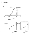
- the measured video signal level - screen brightness characteristic is the characteristic as shown in Fig. 29 (a)
- an inverse curve of the characteristic curve is computed to prepare a correction data as shown in (1) in Fig. 29 (b) (eg., input and output data having 8 bit width).
- the conversion data to be stored in the level conversion RAM 282 for the purpose of the level conversion of the video signal is the linear data as shown in Fig. 29 (c) computed by DDA procedure from the offset value as shown in Fig. 4 (b) as an output from the offset register.
- the total characteristic of the level conversion RAM 282 and look-up-table memory 283 becomes the characteristic as shown in (2) in Fig. 29 (b).
- the video signal level - screen brightness characteristic thereof becomes the characteristic as shown in (2) in Fig. 29 (d), so that, in comparison with the video signal level - screen brightness characteristic [(1) in Fig. 29 (d)] of the case where it has been subjected to the conversion of the look-up-table memory only, fogging of the black level of the video signal can be prevented.
- explanation has been given only on a single color, but the relations are the same with respect to other two colors.
Landscapes
- Engineering & Computer Science (AREA)
- Chemical & Material Sciences (AREA)
- Crystallography & Structural Chemistry (AREA)
- Physics & Mathematics (AREA)
- Computer Hardware Design (AREA)
- General Physics & Mathematics (AREA)
- Theoretical Computer Science (AREA)
- Liquid Crystal Display Device Control (AREA)
- Video Image Reproduction Devices For Color Tv Systems (AREA)
- Control Of Indicators Other Than Cathode Ray Tubes (AREA)
Claims (26)
- Anzeigegerät, das eine Anzeigetafel vom Punktmatrixtyp (15-17, 205-207, 245-247, 265-267) zum Anzeigen eines Videosignals auf einer Basis Pixel für Pixel für einen Punkttakt und für horizontale und vertikale synchrone Signale, und ein Videosignalkompensationsgerät 10, 200, 240, 260 zur Kompensation des Videosignals aufweist,
dadurch gekennzeichnet, daß das Signalkompensationsgerät (10,200) aufweist:
einen Punktzähler (13,23,113,163) zum Zählen des Punkttakts und zum Ausgeben eines ersten Zählsignals, das für eine horizontale Bildschirmposition kennzeichnend ist;
einen Zeilenzähler (14,24,114,164) zum Zählen des horizontalen, synchronen Signals und zum Ausgeben eines zweiten Zählsignals, das für eine vertikale Bildschirmposition kennzeichnend ist;
eine Bildschirmteil-Steuereinrichtung (12,20,110,160) zum Produzieren aus dem ersten und dem zweiten Zählsignal ein Signal, das für einen Bildschirmteilbereich kennzeichnend ist, der einer aus einer Vielzahl Bildschirmteilbereiche in dem gesamten Bildschirm der Anzeigetafel vom Punktmatrixtyp ist; und
eine Korrekturverarbeitungseinrichtung (11,190,201,220,241,261,280), die auf das Signal anspricht, das von der Bildschirmteil-Steuereinrichtung zur Korrektur eines Eingangsvideosignals für jeden der Vielzahl der Teilbereiche basierend auf einer Videosignalpegel-Bildschirmhelligkeitskennlinienkurve der Anzeigetafel vom Punktmatrixtyp in jedem der Vielzahl der Bildschirmteilbereiche entspricht, um so eine Anzeigeungleichmäßigkeit zu korrigieren, die einer Videosignal-Bildschirmhelligkeitskennlinie der Anzeigetafel vom Punktmatrixtyp in jedem der Vielzahl der Bidschirmteilbereiche zugeordnet ist, und ein korrigiertes Videosignal zu der Anzeigetafel vom Punktmatrixtyp ausgibt. - Anzeigegerät nach Anspruch 1, wobei die Bildschirmteil-Steuereinrichtung einen horizontalen Teilbitauswahlschaltkreis, der mit dem Punktzähler zur Auswahl des Bits auf dem oberen Grad als das Bit, das durch die horizontale Teilposition aus den Zählerausgangsbits erneuert werden soll, und einen vertikalen Teilbitauswahlschaltkreis, der mit dem Zeilenzähler zur Auswahl des Bits auf dem oberen Grad als das Bit, das durch die vertikale Teilposition aus den Zählerausgangsbits erneuert werden soll, aufweist, und wobei es die Ausgänge des horizontalen Teilbitauswahlschaltkreises und des vertikalen Teilbitauswahlschaltkreises als die Ausgänge der Bildschirmteilsteuereinrichtung verwendet.
- Anzeigegerät nach Anspruch 1, wobei die Bildschirmteil-Steuereinrichtung einen horizontalen Teilpositionsspeicher, der mit dem Punktzähler zur Erzeugung eines Signals verbunden ist, um die horizontale Teilposition von dem horizontalen Bildschirmpositionssignal zu zeigen, und einen vertikalen Teilpositionsspeicher, der mit dem Punktzähler zur Erzeugung eines Signals verbunden ist, um die vertikale Teilposition von dem vertikalen Bildschirmpositionssignal zu zeigen, aufweist und die Ausgänge des horizontalen Teilpositionsspeichers und des vertikalen Teilpositionsspeichers als die Ausgänge der Bildschirmteil-Steuereinrichtung verwendet.
- Anzeigegerät nach Anspruch 1, wobei die Bildschirmteil-Steuereinrichtung einen horizontalen Teilpositionsspeicher, der mit dem Punktzähler zur Erzeugung eines Signals verbunden ist, um die horizontale Teilposition von der horizontalen Teilposition aus dem horizontalen Bildschirmpositionssignal zu zeigen, einen vertikalen Teilpositionsspeicher, der mit dem Punktzähler zur Erzeugung eines Signals verbunden ist, um die vertikale Teilposition aus dem vertikalen Bildschirmpositionssignal zu erzeugen, und einen Blockadressenspeicher, der mit dem horizontalen Teilpositionsspeicher und dem vertikalen Teilpositionsspeicher zur Erzeugung eines Signals verbunden ist, um den Bildschirmteilbereich aus der horizontalen Teilposition und der vertikalen Teilposition zu zeigen, aufweist, und den Ausgang des Blockadressenspeichers als einen Ausgang der Bildschirmteil-Steuereinrichtung verwendet.
- Anzeigegerät nach Anspruch 1, wobei die Korrekturverarbeitungseinrichtung einen A/D-Wandler zum Konvertieren eines Videosignals in ein digitales Signal, einen Durchsichtstabellenspeicher, der mit dem A/D-Wandler und der Bildschirmteil-Steuereinrichtung zum Speichern der Korrekturdaten für den Bildschirmteilbereich in einer Vielzahl von Tabellen verbunden ist, zum Auswählen der Tabelle durch das Signal von der Bildschirmteilsteuereinrichtung und zum Kompensationskonvertieren des Videosignals von dem A/D-Wandler, und einen D/A-Wandler, der mit der Durchsichtstabelle zum Konvertieren des Ausgangs des Durchsichtstabellenspeichers in ein analoges Signal verbunden ist, aufweist, und wobei der Ausgang des D/A-Wandlers als ein Ausgang der Korrekturverarbeitungseinrichtung verwendet ist.
- Anzeigegerät nach Anspruch 5, wobei die Korrekturdaten, die in der Durchsichtstabelle gespeichert sind, die Daten sind, die durch Messen der Videosignalpegel-Bildschirmhelligkeitskennlinie durch die drei Grundfarben und für den Bildschirmteilbereich und durch Berechnen der inversen Konversionskurve der Kennlinienkurve vorbereitet sind.
- Anzeigegerät nach Anspruch 5, wobei die Korrekturdaten, die in der Durchsichtstabelle gespeichert sind, durch Messen der Videosignalpegel-Bildschirmhelligkeitskennlinie durch die drei Grundfarben und für den Bildschirmteilbereich, durch Berechnen des minimalen Ausgangspegels des maximalen Bildschirmhelligkeitsausgangspegels für den Bildschirmteilbereich und durch Berechnen der inversen Kurve aus der partiellen Kurve von dem Null-Ausgangspegel zu dem minimalen Pegel des Bildschirmhelligkeitsausgangs aus der Kennlinienkurve, vorbereitet sind.
- Anzeigegerät nach Anspruch 5, wobei die Korrekturdaten, die in der Durchsichtstabelle gespeichert sind, Daten sind, die durch Messen der Videosignalpegel-Bildschirmhelligkeitskennlinie durch die drei Grundfarben und durch den Bildschirmteilbereich, durch Berechnen des normalierten Pegels, an dem der gemischte Ausgang der drei Grundfarben des maximalen Bildschirmhelligkeitsausgangspegels durch einen Bildschirmteilbereich eine weiße Farbe wird und durch Berechnen der inversen Konversionskurve aus der partiellen Kurve von dem Null-Ausgangspegel zu dem minimalen Ausgangspegel des Bildschirmhelligkeitsausgangs aus der Kennlinienkurve vorbereitet sind.
- Anzeigegerät nach Anspruch 1, wobei die Korrekturverarbeitungseinrichtung einen A/D-Wandler zum Konvertieren eines Videosignals in ein digitales Signal, einen Blockspeicher, der mit der Bildschirmteil-Steuereinrichtung zum Ausgeben der Korrekturdaten für den Bildschirmteilbereich verbunden ist, einen Multiplier, der mit dem A/D-Wandler und dem Blockspeicher verbunden ist, und einen D/A-Wandler zum Konvertieren des Ausgangs des Multipliers in ein analoges Signal aufweist, und wobei der Ausgang des D/A-Wandlers als ein Ausgang der Korrekturverarbeitungseinrichtung verwendet ist.
- Anzeigegerät nach Anspruch 1, wobei die Korrekturverarbeitungseinrichtung einen A/D-Wandler zum Konvertieren eines Videosignals in ein digitales Signal, einen Blockspeicher, der mit der Bildschirmteil-Steuereinrichtung zum Ausgeben der Korrekturdaten für den Bildschirmteilbereich verbunden ist, einen Addierer, der mit dem A/D-Wandler und dem Blockspeicher verbunden ist, und einen D/A-Wandler zur Konvertierung des Ausgangs des Addierers in ein analoges Signal aufweist, und wobei der Ausgang des D/A-Wandlers als ein Ausgang der Korrekturverarbeitungseinrichtung verwendet wird.
- Anzeigegerät nach Anspruch 1, wobei die Korrekturverarbeitungseinrichtung einen Blockspeicher, der mit der Bildschirmteil-Steuereinrichtung zum Ausgeben der Korrekturdaten für den Bildschirmteilbereich verbunden ist, einen D/A-Wandler, der mit dem Blockspeicher zum Konvertieren der Korrekturdaten in ein analoges Signal verbunden ist, und einen Spannungssteuerverstärker, der mit dem D/A-Wandler zum Verstärken des Videosignals durch den Spannungsausgang des D/A-Wandlers verbunden ist, aufweist, und wobei der Ausgang des Spannungsverstärkers als ein Ausgang der Korrekturverarbeitungseinrichtung verwendet ist.
- Anzeigegerät nach Anspruch 1, wobei die Korrekturverarbeitungseinrichtung einen Blockspeicher, der mit der Bildschirmteil-Steuereinrichtung zum Ausgeben der Korrekturdaten für den Bildschirmteilbereich verbunden ist, einen D/A-Wandler, der mit dem Blockspeicher zum Konvertieren der Korrekturdaten in ein analoges Signal verbunden ist, und einen Spannungsaddierer, der mit dem D/A-Wandler zum Addieren des Spannungsausgangs des D/A-Wandlers in das Videosignal verbunden ist, aufweist, und wobei der Ausgang des Spannungsaddierers als ein Ausgang der Korrekturverarbeitungseinrichtung verwendet ist.
- Anzeigegerät nach Anspruch 1, das weiterhin aufweist: eine Temperaturermittlung (204) zum Messen der Temperatur der Anzeigetafel vom Punktmatrixtyp (205-207); einen A/D-Wandler (203), der mit dem Temperaturdetektor zum Konvertieren des ermittelten Betrags der Temperatur zu einem digitalen Signal verbunden ist; eine Temperatursteuereinrichtung (207), die mit dem A/D-Wandler zum Ausgeben eines Signals für einen Temperaturpegel verbunden ist, wobei die Korrekturverarbeitungseinrichtung (201,220) auf das Ausgangssignal der Temperatursteuereinrichtung zum Korrigieren des Videosignals für den Temperaturpegel anspricht.
- Anzeigegerät nach Anspruch 13, wobei die Temperatursteuereinrichtung einen Temperaturverteilungspositionsspeicher aufweist, der mit dem A/D-Wandler zur Erzeugung eines Signals verbunden ist, das für eine Temperaturverteilungsposition für den Temperaturpegel geeignet ist, und wobei der Ausgang des Temperaturverteilungspositionsspeichers als der Ausgang der Temperatursteuereinrichtung verwendet ist.
- Anzeigegerät nach Anspruch 13, wobei die Korrekturverarbeitungseinrichtung einen A/D-Wandler zum Konvertieren eines Videosignals in ein digitales Signal, einen Durchsichtstabellenspeicher, der mit dem A/D-Wandler und der Temperatursteuereinrichtung zum Speichern der Korrekturdaten für einen Temperaturpegel in einer Vielzahl von Tabellen verbunden ist, zur Auswahl der Tabelle durch das Signal von der Temperatursteuereinrichtung und zur Kompensationskonvertierung des Videosignals von dem A/D-Wandler, einen D/A-Wandler, der mit der Durchsichtstabelle zur Konvertierung des Ausgangs des Durchsichtstabellenspeichers in ein analoges Signal verbunden ist, und einen Spannungsaddierer, der mit dem D/A-Wandler zum Addieren einer spezifischen Spannung verbunden ist, aufweist, und wobei der Ausgang des Spannungsaddierers als ein Ausgang der Korrekturverarbeitungseinrichtung verwendet ist.
- Anzeigegerät nach Anspruch 15, wobei die Korrekturdaten, die in der Durchsichtstabelle gespeichert sind, die Daten sind, die durch Messen der Videosignalpegel-Bildschirmhelligkeitskennlinie für einen individuellen Temperaturpegel der Anzeigetafel vom Punktmatrixtyp für jedes der drei Grundfarbsignale und durch Berechnung der inversen Konvertierungskurve der Kennlinienkurve vorbereitet sind.
- Anzeigegerät nach Anspruch 13, wobei die Korrekturverarbeitungseinrichtung einen A/D-Wandler zum Konvertieren eines Videosignals in ein digitales Signal, einen Durchsichtstabellenspeicher, der mit dem A/D-Wandler zum Speichern von Korrekturdaten in einer Tabelle und zur Kompensationskonvertierung des Videosignals von dem A/D-Wandler zu einer Bitzahl größer als die eingegebene Bitzahl verbunden ist, einen Subtraktionsbetragerzeugungsspeicher zum Ausgeben der Subtraktionsdaten für das Signal von der Temperatursteuereinrichtung, ein Subtrahierglied, das mit dem Durchsichtstabellenspeicher und dem Subtraktionsbetragerzeugungsspeicher verbunden ist, eine Begrenzungseinrichtung, die mit dem Subtrahierglied zum Ausüben einer Begrenzung des Ergebnisses einer Subtraktion verbunden ist, einen D/A-Wandler, der mit der Begrenzungseinrichtung zum Konvertieren des Ausgangs der Begrenzungseinrichtung in ein analoges Signal verbunden ist, und einen Spannungsaddierer, der mit dem D/A-Wandler zum Addieren einer spezifischen Spannung verbunden ist, aufweist, und wobei der Ausgang des Spannungsaddierers als ein Ausgang der Korrekturverarbeitungseinrichtung verwendet ist.
- Anzeigegerät nach Anspruch 1, das weiterhin aufweist: einen spannungsvariablen Schaltkreis (244) zur Erzeugung einer Offsetspannung proportional zu einem vorbestimmten Einstellpegel; einen A/D-Wandler (243), der mit dem spannungsvariablen Schaltkreis zum Konvertieren der Offsetspannung in ein digitales Signal verbunden ist; eine Offsetspannungssteuereinrichtung (242), die mit dem A/D-Wandler zum Ausgeben eines Signals für einen Spannungspegel verbunden ist, wobei die Korrekturverarbeitungseinrichtung (241) auf das Ausgangssignal der Offsetspannungssteuereinrichtung zur Korrektur des Videosignals für den Spannungspegel anspricht.
- Anzeigegerät nach Anspruch 18, wobei die Offsetspannungssteuereinrichtung einen Spannungsverteilungspositionsspeicher aufweist, der mit dem A/D-Wandler zur Erzeugung eines Signals verbunden ist, um die Spannungsverteilungsposition von dem Spannungspegel darzustellen, und wobei der Ausgang des Spannungsverteilungspositionsspeichers als ein Ausgang der Offsetspannungsssteuereinrichtung verwendet ist.
- Anzeigegerät nach Anspruch 18, wobei die Korrekturverarbeitungseinrichtung einen A/D-Wandler zum Konvertieren eines Videosignals in ein digitales Signal, einen Durchsichtstabellenspeicher, der mit einem A/D-Wandler und der Offsetspannungssteuereinrichtung zur Speicherung der Korrekturdaten für einen Temperaturpegel in einer Vielzahl Tabellen verbunden ist, zur Auswahl der Tabelle durch das Signal von der Offsetspannungssteuereinrichtung und zur Kompensationskonvertierung des Videosignals von dem A/D-Wandler, einen D/A-Wandler, der mit dem Durchsichtstabellenspeicher zur Konvertierung des Ausgangs des Durchsichtstabellenspeichers in ein analoges Signal verbunden ist, einen Spannungsaddierer, der mit dem D/A-Wandler und dem spannungsvariablen Schaltkreis zum Addieren einer Offsetspannung zu dem Ausgang des D/A-Wandlers verbunden ist, und einen Spannungsaddierer, der mit dem Spannungsaddierer zum Addieren einer spezifischen Spannung verbunden ist, aufweist, und wobei der Ausgang des Spannungsaddierers als ein Ausgang der Korrekturverarbeitungseinrichtung verwendet ist.
- Anzeigegerät nach Anspruch 20, wobei die Korrekturdaten, die in der Durchsichtstabelle gespeichert sind, die Daten sind, die durch Messen der Videosignalpegel-Bildschirmhelligkeitskennlinie durch einen individuellen Spannungspegel der Anzeigetafel vom Punktmatrixtyp für jede der drei Grundfarbsignale und durch Berechnung der inversen Konversions-Kennlinienkurve vorbereitet sind.
- Anzeigegerät nach Anspruch 1, das weiterhin aufweist: ein Offsetregister zum Ausgeben eines Offsetwerts proportional zu einem vorbestimmten Einstellpegel, wobei die Korrekturverarbeitungseinrichtung (261,280) auf den Offsetwert zur Korrektur des Videosignals durch den Offsetwert anspricht.
- Anzeigegerät nach Anspruch 22, wobei die Korrekturverarbeitungseinrichtung einen A/D-Wandler zum Konvertieren eines Videosignals in ein digitales Signal, einen Durchsichtstabellenspeicher, der mit dem D/A-Wandler zur Speicherung der Korrekturdaten in einer Tabelle verbunden ist, und zur Kompensationskonvertierung des Videosignals von dem A/D-Wandler, einen Addierer, der mit dem Durchsichtstabellenspeicher und dem Offsetregister verbunden ist, eine Begrenzungseinrichtung, die mit dem Addierer zum Ausüben einer Begrenzung des Ergebnisses einer Addition verbunden ist, und einen D/A-Wandler, der mit der Begrenzungseinrichtung zum Konvertieren des Ausgangs der Begrenzungseinrichtung in ein analoges Signal verbunden ist, aufweist, und wobei der Ausgang des D/A-Wandlers als ein Ausgang der Korrekturverarbeitungseinrichtung verwendet ist.
- Anzeigegerät nach Anspruch 23, wobei die Korrekturdaten, die in der Durchsichtstabelle gespeichert sind, Daten sind, die durch Messen der Videosignalpegel-Bildschirmhelligkeitskennlinie der Anzeigetafel vom Punktmatrixtyp für jede der drei Grundfarbsignale und durch Berechnung der inversen Kurve der Kennlinienkurve vorbereitet sind.
- Anzeigegerät nach Anspruch 22, wobei die Korrekturverarbeitungseinrichutng einen A/D-Wandler zum Konvertieren eines Videosignals in ein digitales Signal, einen Pegelkonvertierungs-RAM, der mit dem A/D-Wandler zum Speichern der Konversionsdaten zum Ändern der Pegelverteilung des Videosignals und zur Pegelkonvertierung des Videosignals von dem A/D-Wandler verbunden ist, einen Durchsichtstabellenspeicher, der mit dem Pegelkonvertierungs-RAM zum Speichern der Korrekturdaten in der Tabelle und zur Kompensationskonvertierung des Videosignals von dem Konversions-RAM verbunden ist, einen D/A-Wandler, der mit dem Durchsichtstabellenspeicher zum Konvertieren des Ausgangs des Durchsichtstabellenspeichers in ein analoges Signal verbunden ist, einen Linearzeilenerzeugungsschaltkreis, der mit dem Offsetregister zur Erzeugung einer linearen Zeile, deren Gradient gemäß dem Offsetwert variiert, verbunden ist, und zur Berechnung der Konvertierungsdaten und zum Ausgeben zu dem Pegelkonvertierungs-RAM verbunden ist, und einen RAM-Einschreibsteuerschaltkreis, der mit dem linearen Zeilenerzeugungsschaltkreis zum Ausgeben eines Einschreibsteuersignals zu dem Pegelkonvertierungs-RAM durch das Signal eines Abschlusses einer Berechnung der Konvertierungsdaten verbunden ist, und wobei der Ausgang des D/A-Wandlers als der Ausgang der Korrekturverarbeitungseinrichtung verwendet ist.
- Anzeigegerät nach Anspruch 25, wobei die Korrekturdaten, die in der Durchsichtstabelle gespeichert sind, die Daten sind, die durch Messung der Videosignalpegel-Bildschirmhelligkeitskennlinie einer Anzeigetafel vom Punktmatrixtyp für jedes der drei Grundfarbsignale und durch Berechnung der inversen Konversionskurve der Kennlinienkurve vorbereitet sind.
Applications Claiming Priority (4)
| Application Number | Priority Date | Filing Date | Title |
|---|---|---|---|
| JP1153391A JP2512152B2 (ja) | 1989-06-15 | 1989-06-15 | 映像信号補正装置 |
| JP153391/89 | 1989-06-15 | ||
| JP175854/89 | 1989-07-07 | ||
| JP1175854A JPH0340674A (ja) | 1989-07-07 | 1989-07-07 | ドットマトリクス表示装置 |
Publications (3)
| Publication Number | Publication Date |
|---|---|
| EP0403268A2 EP0403268A2 (de) | 1990-12-19 |
| EP0403268A3 EP0403268A3 (de) | 1992-08-19 |
| EP0403268B1 true EP0403268B1 (de) | 1995-10-11 |
Family
ID=26482024
Family Applications (1)
| Application Number | Title | Priority Date | Filing Date |
|---|---|---|---|
| EP90306463A Expired - Lifetime EP0403268B1 (de) | 1989-06-15 | 1990-06-13 | Gerät zur Kompensierung von Videosignalen |
Country Status (3)
| Country | Link |
|---|---|
| US (1) | US5359342A (de) |
| EP (1) | EP0403268B1 (de) |
| DE (1) | DE69022891T2 (de) |
Families Citing this family (52)
| Publication number | Priority date | Publication date | Assignee | Title |
|---|---|---|---|---|
| EP0462333B1 (de) * | 1990-06-11 | 1994-08-31 | International Business Machines Corporation | Anzeigeeinrichtung |
| FR2678462B1 (fr) * | 1991-06-25 | 1993-12-24 | Sextant Avionique | Dispositif temps reel de presentation d'images de type television sur un ecran de visualisation. |
| US5495287A (en) | 1992-02-26 | 1996-02-27 | Hitachi, Ltd. | Multiple-tone display system |
| JP3672586B2 (ja) * | 1994-03-24 | 2005-07-20 | 株式会社半導体エネルギー研究所 | 補正システムおよびその動作方法 |
| US5703621A (en) * | 1994-04-28 | 1997-12-30 | Xerox Corporation | Universal display that presents all image types with high image fidelity |
| US5668577A (en) * | 1994-08-12 | 1997-09-16 | Sutter; Erich E. | Video circuit for generating special fast dynamic displays |
| FR2726144B1 (fr) * | 1994-10-24 | 1996-11-29 | Valeo Vision | Procede et dispositif d'amelioration de la vision nocturne, notamment pour vehicule automobile |
| KR960024524A (ko) * | 1994-12-21 | 1996-07-20 | 김광호 | 기억소자를 이용한 액정 표시장치의 감마 보정장치 |
| JP3309738B2 (ja) * | 1996-11-01 | 2002-07-29 | 松下電器産業株式会社 | 画像表示装置 |
| US6020868A (en) * | 1997-01-09 | 2000-02-01 | Rainbow Displays, Inc. | Color-matching data architectures for tiled, flat-panel displays |
| CN1145064C (zh) * | 1997-04-18 | 2004-04-07 | 精工爱普生株式会社 | 电光装置及其驱动电路、驱动方法和相关电子设备 |
| US6320592B1 (en) * | 1997-06-30 | 2001-11-20 | Sun Microsystems, Inc. | Method and apparatus for separating image data from a color system in image processing |
| TW522354B (en) * | 1998-08-31 | 2003-03-01 | Semiconductor Energy Lab | Display device and method of driving the same |
| US6438273B1 (en) * | 1998-12-23 | 2002-08-20 | Xerox Corporation | Method and apparatus for using rotatable templates within look-up tables to enhance image reproduction |
| US6670938B1 (en) * | 1999-02-16 | 2003-12-30 | Canon Kabushiki Kaisha | Electronic circuit and liquid crystal display apparatus including same |
| JP3632505B2 (ja) | 1999-06-18 | 2005-03-23 | セイコーエプソン株式会社 | 画像表示装置 |
| US6876339B2 (en) * | 1999-12-27 | 2005-04-05 | Semiconductor Energy Laboratory Co., Ltd. | Semiconductor device and driving method thereof |
| JP3763397B2 (ja) * | 2000-03-24 | 2006-04-05 | シャープ株式会社 | 画像処理装置、画像表示装置、パーソナルコンピュータ、画像処理方法 |
| US7030846B2 (en) * | 2001-07-10 | 2006-04-18 | Samsung Electronics Co., Ltd. | Color correction liquid crystal display and method of driving same |
| DE10158541A1 (de) * | 2001-11-29 | 2003-06-12 | Siemens Ag | Schaltungsanordnung zur Ansteuerung eines monochromen Flachbildschirms und Verfahren zur Verminderung der Wolkigkeit eines monochromen Flachbildschirms sowie Flachbildschirm |
| US7129920B2 (en) * | 2002-05-17 | 2006-10-31 | Elcos Mircrodisplay Technology, Inc. | Method and apparatus for reducing the visual effects of nonuniformities in display systems |
| EP1367558A3 (de) * | 2002-05-29 | 2008-08-27 | Matsushita Electric Industrial Co., Ltd. | Bildanzeigeverfahren und Vorrichtung mit Luminanzseinstellung einer Lichtquelle |
| EP1424672A1 (de) * | 2002-11-29 | 2004-06-02 | Barco N.V. | Verfahren und Vorrichtung zur Korrektur von Ungleichmässigkeiten von Pixeln einer Matrixanzeige |
| WO2005015533A1 (en) * | 2003-08-11 | 2005-02-17 | Koninklijke Philips Electronics, N.V. | Uniformity correction of black and white states in liquid crystal displays |
| JP4114655B2 (ja) * | 2003-11-12 | 2008-07-09 | セイコーエプソン株式会社 | 輝度ムラの補正方法、輝度ムラの補正回路、電気光学装置および電子機器 |
| US7420538B2 (en) * | 2003-12-03 | 2008-09-02 | Sharp Kabushiki Kaisha | Liquid crystal display device and driving device thereof, and method for driving liquid crystal display device |
| JP4834295B2 (ja) * | 2004-01-09 | 2011-12-14 | 株式会社東芝 | 映像表示装置および映像表示方法 |
| EP1587049A1 (de) * | 2004-04-15 | 2005-10-19 | Barco N.V. | Verfahren und Vorrichtung zur Verbesserung der Übereinstimmung einer Anzeigetafel mit einem Anzeigestandard vollflächig und für verschiedene Blickwinkel |
| EP1645798B1 (de) | 2004-09-15 | 2012-03-28 | Research In Motion Limited | Verfahren und Vorrichtung zur Herstellung einer gleichmässigen Rückbeleuchtung |
| US7113670B2 (en) * | 2004-09-15 | 2006-09-26 | Research In Motion Limited | Method and device to improve backlight uniformity |
| DE602004024895D1 (de) | 2004-10-25 | 2010-02-11 | Barco Nv | Optische Korrektur für Leuchtpaneele mit hoher Gleichmäßigkeit |
| KR100593537B1 (ko) * | 2005-03-22 | 2006-06-28 | 엘지전자 주식회사 | 플라즈마 디스플레이 패널의 화질 개선을 위한신호처리장치 및 그 방법 |
| US7639849B2 (en) | 2005-05-17 | 2009-12-29 | Barco N.V. | Methods, apparatus, and devices for noise reduction |
| DE102005028916A1 (de) * | 2005-06-22 | 2007-01-04 | Siemens Ag | Verfahren zum Einstellen der Leuchtdichte eines auf einer LCD-Anzeige eines LCD-Displaymoduls darstellbaren Bildes |
| TWI276864B (en) * | 2005-12-16 | 2007-03-21 | Innolux Display Corp | Display system |
| KR20070118371A (ko) * | 2006-06-12 | 2007-12-17 | 삼성전자주식회사 | 디스플레이장치 및 그 제어방법 |
| US20080117231A1 (en) | 2006-11-19 | 2008-05-22 | Tom Kimpe | Display assemblies and computer programs and methods for defect compensation |
| RU2468450C2 (ru) * | 2007-07-11 | 2012-11-27 | Сони Корпорейшн | Устройство дисплея и способ управления устройством дисплея |
| CN101765874B (zh) * | 2008-05-28 | 2014-09-10 | 松下电器产业株式会社 | 显示装置、显示装置的制造方法及控制方法 |
| JP2010127994A (ja) * | 2008-11-25 | 2010-06-10 | Sony Corp | 補正値算出方法、表示装置 |
| CN106375553B (zh) * | 2016-08-24 | 2019-09-17 | 武汉华星光电技术有限公司 | 显示屏组合及具有该显示屏组合的移动终端 |
| US11030942B2 (en) | 2017-10-13 | 2021-06-08 | Jasper Display Corporation | Backplane adaptable to drive emissive pixel arrays of differing pitches |
| US10951875B2 (en) | 2018-07-03 | 2021-03-16 | Raxium, Inc. | Display processing circuitry |
| US11710445B2 (en) | 2019-01-24 | 2023-07-25 | Google Llc | Backplane configurations and operations |
| US11637219B2 (en) | 2019-04-12 | 2023-04-25 | Google Llc | Monolithic integration of different light emitting structures on a same substrate |
| US11238782B2 (en) | 2019-06-28 | 2022-02-01 | Jasper Display Corp. | Backplane for an array of emissive elements |
| US11626062B2 (en) | 2020-02-18 | 2023-04-11 | Google Llc | System and method for modulating an array of emissive elements |
| WO2021207129A1 (en) | 2020-04-06 | 2021-10-14 | Raxium, Inc. | Display assemblies |
| US11538431B2 (en) | 2020-06-29 | 2022-12-27 | Google Llc | Larger backplane suitable for high speed applications |
| US12573349B2 (en) | 2020-06-29 | 2026-03-10 | Google Llc | Efficient image data delivery for an array of pixel memory cells |
| JP7720395B2 (ja) | 2020-12-21 | 2025-08-07 | グーグル エルエルシー | オートビュー3dディスプレイ用の高密度画素アレイ |
| TW202303555A (zh) | 2021-07-14 | 2023-01-16 | 美商谷歌有限責任公司 | 用於脈寬調變的背板和方法 |
Family Cites Families (17)
| Publication number | Priority date | Publication date | Assignee | Title |
|---|---|---|---|---|
| JPS5917430B2 (ja) * | 1977-10-31 | 1984-04-21 | シャープ株式会社 | マトリツクス型液晶表示装置 |
| US4386345A (en) * | 1981-09-22 | 1983-05-31 | Sperry Corporation | Color and brightness tracking in a cathode ray tube display system |
| JPS6194087A (ja) * | 1984-10-15 | 1986-05-12 | 松下電器産業株式会社 | 表示装置 |
| JPH0680477B2 (ja) * | 1985-02-06 | 1994-10-12 | キヤノン株式会社 | 液晶表示パネル及び駆動方法 |
| JPS61213896A (ja) * | 1985-03-19 | 1986-09-22 | 株式会社 アスキ− | デイスプレイコントロ−ラ |
| JPS61219023A (ja) * | 1985-03-23 | 1986-09-29 | Sharp Corp | 液晶表示装置 |
| JPS61243495A (ja) * | 1985-04-20 | 1986-10-29 | 三洋電機株式会社 | 液晶表示装置の表示むら補償方法 |
| US4827255A (en) * | 1985-05-31 | 1989-05-02 | Ascii Corporation | Display control system which produces varying patterns to reduce flickering |
| US4825201A (en) * | 1985-10-01 | 1989-04-25 | Mitsubishi Denki Kabushiki Kaisha | Display device with panels compared to form correction signals |
| JPS62209418A (ja) * | 1986-03-10 | 1987-09-14 | Fujitsu Ltd | アクテイブマトリクス型液晶表示装置 |
| JPS6337785A (ja) * | 1986-07-31 | 1988-02-18 | Toshiba Electric Equip Corp | 映像表示装置 |
| JPS63148781A (ja) * | 1986-12-12 | 1988-06-21 | Nec Corp | 液晶表示装置 |
| JPS63270167A (ja) * | 1987-04-30 | 1988-11-08 | Fuji Photo Film Co Ltd | 画像形成方法 |
| GB2207271B (en) * | 1987-06-15 | 1991-06-05 | Graphic Forming Ltd | Resilient edging strip and display panel |
| JP2906057B2 (ja) * | 1987-08-13 | 1999-06-14 | セイコーエプソン株式会社 | 液晶表示装置 |
| US4888599A (en) * | 1987-10-23 | 1989-12-19 | Rockwell International Corp. | Real time apparatus for adjusting contrast ratio of liquid crystal displays |
| ATE116466T1 (de) * | 1987-10-26 | 1995-01-15 | Canon Kk | Treiberschaltung. |
-
1990
- 1990-06-13 DE DE69022891T patent/DE69022891T2/de not_active Expired - Fee Related
- 1990-06-13 EP EP90306463A patent/EP0403268B1/de not_active Expired - Lifetime
-
1993
- 1993-02-01 US US08/011,828 patent/US5359342A/en not_active Expired - Fee Related
Also Published As
| Publication number | Publication date |
|---|---|
| EP0403268A2 (de) | 1990-12-19 |
| US5359342A (en) | 1994-10-25 |
| DE69022891D1 (de) | 1995-11-16 |
| EP0403268A3 (de) | 1992-08-19 |
| DE69022891T2 (de) | 1996-05-15 |
Similar Documents
| Publication | Publication Date | Title |
|---|---|---|
| EP0403268A2 (de) | Gerät zur Kompensierung von Videosignalen | |
| TWI859379B (zh) | 色差補償電路及應用該色差補償電路的用於顯示器的驅動裝置 | |
| US6765551B2 (en) | Column electrode driving circuit for use with image display device and image display device incorporating the same | |
| CN101317212B (zh) | 用于驱动显示元件的显示设备和方法 | |
| JP3277121B2 (ja) | 液晶デイスプレイの中間表示駆動方式 | |
| US7202879B2 (en) | Image processing method, image processing apparatus, electronic device, image processing program, and recording medium on which the same program is recorded | |
| JP2512152B2 (ja) | 映像信号補正装置 | |
| CN110189720B (zh) | 四色像素的白平衡参数生成方法和显示装置 | |
| KR20150081085A (ko) | 표시 패널의 영상 보정 방법, 이를 포함하는 표시 패널의 구동 방법 및 이를 수행하기 위한 표시 장치 | |
| US6489938B1 (en) | Matrix display apparatus and plasma addressed display apparatus | |
| CN118016017B (zh) | 显示面板的显示补偿方法、装置及显示设备 | |
| KR20030093129A (ko) | 화상 처리 장치, 화상 처리 방법, 화상 표시 장치, 및이동 전자 기기 | |
| WO2024178902A1 (zh) | 显示面板的亮度补偿方法及亮度补偿装置及显示装置 | |
| KR100363021B1 (ko) | 디스플레이장치 | |
| CN116844485B (zh) | 显示屏电压降补偿方法、装置、设备及存储介质 | |
| US11900854B1 (en) | Display device and method for driving display panel | |
| US7663678B2 (en) | Gamma correction, image processing method and program, gamma correction circuit, image processing apparatus, and display apparatus | |
| US11450295B2 (en) | Charge compensation circuit, charge compensation method, and display device | |
| US20120001959A1 (en) | Electro-optical device, image processing circuit, and electronic device | |
| TW202125473A (zh) | 色差補償電路及應用該色差補償電路的用於顯示器的驅動裝置 | |
| KR100810567B1 (ko) | 디더링에 의한 액정온실리콘 디스플레이에서의 윤곽의 감소 | |
| US20070109321A1 (en) | Method for compensating a brightness error of a flat panel display | |
| KR100463412B1 (ko) | 의사계조를 표시하는 표시장치 및 이를 표시하는 표시방법 | |
| CN100479486C (zh) | 自动图像修正电路 | |
| CN1971683A (zh) | 平面显示器的亮度补偿方法 |
Legal Events
| Date | Code | Title | Description |
|---|---|---|---|
| PUAI | Public reference made under article 153(3) epc to a published international application that has entered the european phase |
Free format text: ORIGINAL CODE: 0009012 |
|
| AK | Designated contracting states |
Kind code of ref document: A2 Designated state(s): DE FR GB |
|
| PUAL | Search report despatched |
Free format text: ORIGINAL CODE: 0009013 |
|
| AK | Designated contracting states |
Kind code of ref document: A3 Designated state(s): DE FR GB |
|
| 17P | Request for examination filed |
Effective date: 19930215 |
|
| 17Q | First examination report despatched |
Effective date: 19940502 |
|
| GRAA | (expected) grant |
Free format text: ORIGINAL CODE: 0009210 |
|
| AK | Designated contracting states |
Kind code of ref document: B1 Designated state(s): DE FR GB |
|
| REF | Corresponds to: |
Ref document number: 69022891 Country of ref document: DE Date of ref document: 19951116 |
|
| ET | Fr: translation filed | ||
| PLBE | No opposition filed within time limit |
Free format text: ORIGINAL CODE: 0009261 |
|
| STAA | Information on the status of an ep patent application or granted ep patent |
Free format text: STATUS: NO OPPOSITION FILED WITHIN TIME LIMIT |
|
| 26N | No opposition filed | ||
| PGFP | Annual fee paid to national office [announced via postgrant information from national office to epo] |
Ref country code: GB Payment date: 19990609 Year of fee payment: 10 |
|
| PGFP | Annual fee paid to national office [announced via postgrant information from national office to epo] |
Ref country code: FR Payment date: 19990610 Year of fee payment: 10 |
|
| PGFP | Annual fee paid to national office [announced via postgrant information from national office to epo] |
Ref country code: DE Payment date: 19990614 Year of fee payment: 10 |
|
| PG25 | Lapsed in a contracting state [announced via postgrant information from national office to epo] |
Ref country code: GB Free format text: LAPSE BECAUSE OF NON-PAYMENT OF DUE FEES Effective date: 20000613 |
|
| GBPC | Gb: european patent ceased through non-payment of renewal fee |
Effective date: 20000613 |
|
| PG25 | Lapsed in a contracting state [announced via postgrant information from national office to epo] |
Ref country code: FR Free format text: LAPSE BECAUSE OF NON-PAYMENT OF DUE FEES Effective date: 20010228 |
|
| REG | Reference to a national code |
Ref country code: FR Ref legal event code: ST |
|
| PG25 | Lapsed in a contracting state [announced via postgrant information from national office to epo] |
Ref country code: DE Free format text: LAPSE BECAUSE OF NON-PAYMENT OF DUE FEES Effective date: 20010403 |