EP0403836A1 - Schieberegister zur Erzeugung von Impulsen in Sequenz - Google Patents
Schieberegister zur Erzeugung von Impulsen in Sequenz Download PDFInfo
- Publication number
- EP0403836A1 EP0403836A1 EP90110160A EP90110160A EP0403836A1 EP 0403836 A1 EP0403836 A1 EP 0403836A1 EP 90110160 A EP90110160 A EP 90110160A EP 90110160 A EP90110160 A EP 90110160A EP 0403836 A1 EP0403836 A1 EP 0403836A1
- Authority
- EP
- European Patent Office
- Prior art keywords
- shift
- data
- node
- terminal
- clock signal
- Prior art date
- Legal status (The legal status is an assumption and is not a legal conclusion. Google has not performed a legal analysis and makes no representation as to the accuracy of the status listed.)
- Granted
Links
- 230000008878 coupling Effects 0.000 claims 2
- 238000010168 coupling process Methods 0.000 claims 2
- 238000005859 coupling reaction Methods 0.000 claims 2
- 239000003990 capacitor Substances 0.000 description 3
- 230000000295 complement effect Effects 0.000 description 3
- 238000010586 diagram Methods 0.000 description 3
- 238000005070 sampling Methods 0.000 description 2
- 239000000470 constituent Substances 0.000 description 1
- 238000010276 construction Methods 0.000 description 1
- 230000005236 sound signal Effects 0.000 description 1
Images


Classifications
-
- G—PHYSICS
- G11—INFORMATION STORAGE
- G11C—STATIC STORES
- G11C19/00—Digital stores in which the information is moved stepwise, e.g. shift registers
- G11C19/28—Digital stores in which the information is moved stepwise, e.g. shift registers using semiconductor elements
-
- G—PHYSICS
- G11—INFORMATION STORAGE
- G11C—STATIC STORES
- G11C19/00—Digital stores in which the information is moved stepwise, e.g. shift registers
Definitions
- the present invention relates to a shiftregister for shifting a data therethrough in synchronism with a shift clock signal and, more particularly, to a shiftregister used for producing a plurality of continuous pulses in accordance with shifting a data therethrough in synchronism with a shift clock signal.
- a shiftregister is composed of a plurality of a data-shift stages connected in cascade.
- Each of the data-shift stages temporarily holds a data supplied thereto from a preceding stage in synchronism with one of leading and trailing edges of an clock pulse signal.
- the data holding stage produces an output during adjacent two leading or trailing edges of the clock pulse signal. Thereafter, the data holding stage supplies its data to succeeding stage. Accordingly, the shiftregister shifts an input data supplied to the leading data-shift stage toward the last data-shift stage successively in synchronism with the shift clock signal.
- a plurality of pulses generating in sequence can be derived from the shiftregister by providing terminals on respective stages, each of which connects to the succeeding data-shift stage.
- These pulses thus derived can be used as drive pulses for driving transistors.
- An example is to drive transistors for sampling an analog signal such as video signal or audio signal in time sequence.
- Another is to drive transistors for designating a digit or a row to be display in a display panel.
- each of the data-shift stages derives the data in synchronism with the same leading or trailing edges of the shift clock signal, the trailing edge portion of the driving pulse generated from one data-shift stage may overlaps with the leading edge portion of the driving pulse generated from the succeeding data-shift stage. For this reason, there may occur a time period during which two stages both generate drive pulses. This causes that the analog signal is not sampled accurately and two digits or rows of the display panel are simultaneously designated to be displayed.
- an object of the present invention is to provide an improved shiftregister for producing a plurality of pulses in sequence, especially for generating the plurality of pulses without overlapping any portions of consequtive pulses with each other.
- a shiftregister comprises a plurality of data-shift stages connected in cascade, each of which includes a shift-in terminal, a shift-out terminal, first, second and third nodes, a first transfer gate connected between the shift-in terminal and the first node and opened during one logic level period of a shift clock signal, a first hold circuit connected between the first and second nodes to hold a level at the first node during the other logic level period of the shift clock signal, a second transfer gate connected between the second and third nodes and opened during the other logic level period of the shift clock signal, a second hold circuit connected between the third node and the shift-out terminal to hold a level at the third node during one logic level period of the shift clock signal, and a gate circuit coupled to selected ones of the shift-in and shift-out terminals and the first to third node and producing a pulse signal when logic levels at the selected ones are in a predetermined logic level state.
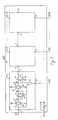
- a shiftregister 100 includes N pieces of data-shift stages 10-1, 10-2, ..., 10-N each including a shift-in terminal 6 and a shift-out terminal 7. These data-shift stages 10-1 to 10-N are coupled in cascade in such a manner that the shift-out terminal 7 of the preceding data-shift stage, 10-1 for example, is connected to the shift-in terminal 6 of the succeeding data-shift stage, i.e. 10-2. However, the shift-in terminal 6 of the leading data-shift stage 10-1 is supplied with input data DI to be shifted.
- the shiftregister 100 is further supplied with a shift clock signal ⁇ .
- An inverter 9 inverts the phase of the shift clock signal ⁇ to produce a complementary shift clock signal ⁇ .
- Each of the data-shift stages 10-1 to 10-N includes a first transfer gate 1 connected between the shift-in terminal 6 and a first node N1, a first data hold circuit 2 connected between the first node N1 and a second node N2, a second transfer gate 3 connected between the second node N2 and a third node N3, and a second data hold circuit 4 connected between the third node N3 and the shift-out terminal 7.
- the first and second transfer gates 1 and 3 are composed of a pair of P-channel and N-channel MOS transistors 1P and 1N and 3P and 3N connected in parallel, respectively.
- the true shift clock signal ⁇ is supplied to the gates of the transistors 1P and 3N and the complementary shift clock signal ⁇ is supplied to the gates of the transistor 1N and 3P. Therefore, the first and second transfer gates 1 and 3 are made open during the low level period and during the high level period of the shift clock signal ⁇ , respectively.
- the first and second data hold circuits 2 and 4 are composed of a pair of inverters 21 and 22 and 41 and 42, respectively, connected in such a manner that the input and output of one inverter 21 or 41 are connected respectively to the output and input of the other inverter 22 and 42.
- the inverters 22 and 42 are of a well-kown clocked-type controlled by the shift clock signals ⁇ and ⁇ .
- the clocked-inverter 22 thus operates during the high level period of the shift clock ⁇ , while the clocked-inverter 24 operates during the low level period thereof. Accordingly, the data hold circuit 2 outputs the inverted data of the data at the node N1 during the low level period of the shift clock signal ⁇ and holds the inverted data during the high level period thereof. On the other hand, the data hold circuit 4 outputs the inverted data of the data at the node N3 during the high level period of the shift clock signal ⁇ and holds the inverted data during the low level period thereof.
- Each of the data-shift stages 10-1 to 10-N further includes a drive pulse output terminal 8 and a NOR gate 5 in accordance with the present invention.
- the NOR gate 5 has a first input node connected to the shift-in terminal 6, a second input node connected to the node N3 and an output node connected to the drive pulse output terminal 8 from which a corresponding one of drive pulses DP1 to DPN is derived.
- the transfer gate 1 In response to the change of the shift clock ⁇ to the high level, the transfer gate 1 is closed and the inverter 22 is activated. Therefore, the nodes N1 and N2 are maintained at the high level and the low level, respectively.
- the transfer gate 3 is made open and the inverter 42 is deactivated, so that the node N3 and the shift-out terminal 7 are changed to the low level and the high level, respectively.
- the node N3 and the shift-out terminal 7 change to the high level and low level, respectively.
- the respective levels at nodes N1, N2 and N3 and the shift-out terminal 7 are maintained until the next input data of the high level is supplied to the shift-in terminal 6.
- the shift-out terminal 7 of the second data-shift stage 10-2 changes to the high level in response to the above succeeding change of the shift clock signal ⁇ to the high level and then changes to the low level in response to a further succeeding change of the signal ⁇ to the high level, as shown in Fig. 2.
- the third data-shift stage 10-3 starts to change the shift-out terminal 7 thereof to the high level.
- the input data DI of the high level is shifted from the leading data-shift stage 10-1 to the last data-shift stage 10-N in order in synchronism with the shift clock signal ⁇ . Since a sequence of pulses are derived from the shift-out terminals 7 of the data-shift stages 10-1 to 10-N, those pulses can be also used as drive pulses. However, as shown by "OT" in Fig. 2, the trailing edge portion of one shift-out pulse overlaps with the leading edge portion of the succeeding shift-out pulse.
- the NOR gate receives the data signals at the shift-in terminal 6 and the node N3 and outputs the drive pulse DP to the terminal 8.
- the drive pulse DP take the high level.
- the drive pulse DP takes the low level.
- the data-shift stages 10-1 to 10-N produce drive pulses DP1 to DPN in order without overlap of successive two pulses, as shown in Fig. 2.
- the shiftregister shown in Fig. 1 is applied to a signal sample and hold circuit.
- An analog signal AI including video information is supplied in common to the respective one ends of N-channel MOS transistors Q1 to Q N which are in turn controlled by the drive pulses DP1 to DPN from the shiftregister 100, respectively.
- the other ends of the transistors Q1 to Q N are connected to capacitors C1 to C N , respectively.
- the transistor Q1 is turned ON by the corresponding drive pulse DP1
- the level of the signal AI is sampled and held by the capacitor C1.
- the level of the signal AI is thus sampled and held in time sequence.
- the level of the signal AI is sampled precisely. If the shift-out pulses at the terminals 7 are used us the drive pulses DP, two transistors, Q1 and Q2 for example, are turned ON during the period OT shown in Fig. 2, so that the level of the signal AI is subjected to the capacitance-division by the capacitors C1 and C2, the precise level sampling operation being thereby performed.
- Fig. 3 there is shown another embodiment of the present invention, in which the same constituents as those shown in Fig. 1 are denoted by the same reference numerals to omit the further description thereof.
- the first input node of the NOR gate 5 is connected to the node N1. Therefore, a sequence of drive pulses DP1 to DPN are produced in accordance with the timing shown in Fig. 4.
- each of the drive pulses DP1 to DPN are completely separated from one another.
- the pulse width of each drive pulse DP can be controlled by the low level period of the shift clock signal ⁇ .
Landscapes
- Shift Register Type Memory (AREA)
- Liquid Crystal Display Device Control (AREA)
- Control Of Indicators Other Than Cathode Ray Tubes (AREA)
Applications Claiming Priority (2)
| Application Number | Priority Date | Filing Date | Title |
|---|---|---|---|
| JP137099/89 | 1989-05-30 | ||
| JP1137099A JP2639105B2 (ja) | 1989-05-30 | 1989-05-30 | Mos型シフトレジスタ |
Publications (2)
| Publication Number | Publication Date |
|---|---|
| EP0403836A1 true EP0403836A1 (de) | 1990-12-27 |
| EP0403836B1 EP0403836B1 (de) | 1995-08-16 |
Family
ID=15190837
Family Applications (1)
| Application Number | Title | Priority Date | Filing Date |
|---|---|---|---|
| EP90110160A Expired - Lifetime EP0403836B1 (de) | 1989-05-30 | 1990-05-29 | Schieberegister zur Erzeugung von Impulsen in Sequenz |
Country Status (4)
| Country | Link |
|---|---|
| US (1) | US5099502A (de) |
| EP (1) | EP0403836B1 (de) |
| JP (1) | JP2639105B2 (de) |
| DE (1) | DE69021649T2 (de) |
Cited By (1)
| Publication number | Priority date | Publication date | Assignee | Title |
|---|---|---|---|---|
| GB2310062A (en) * | 1996-02-08 | 1997-08-13 | Hyundai Electronics Ind | Memory device and address register therefor |
Families Citing this family (3)
| Publication number | Priority date | Publication date | Assignee | Title |
|---|---|---|---|---|
| JP4956506B2 (ja) | 2008-08-08 | 2012-06-20 | 株式会社東芝 | シフトレジスタ |
| TWI525615B (zh) | 2011-04-29 | 2016-03-11 | 半導體能源研究所股份有限公司 | 半導體儲存裝置 |
| JP6899344B2 (ja) | 2018-02-22 | 2021-07-07 | 株式会社東芝 | 放射線検出器 |
Citations (2)
| Publication number | Priority date | Publication date | Assignee | Title |
|---|---|---|---|---|
| US3578984A (en) * | 1967-12-14 | 1971-05-18 | Plessey Co Ltd | Master/slave switching circuit employing insulated-gate field-effect transistors |
| EP0147103A2 (de) * | 1983-12-05 | 1985-07-03 | Texas Instruments Incorporated | MOS-Durchführung eines Schieberegisterverrieglers |
Family Cites Families (4)
| Publication number | Priority date | Publication date | Assignee | Title |
|---|---|---|---|---|
| US3862440A (en) * | 1972-09-14 | 1975-01-21 | Tokyo Shibaura Electric Co | Pulse transforming circuit arrangements using a clock pulse responsive delayed inverter means |
| US4495628A (en) * | 1982-06-17 | 1985-01-22 | Storage Technology Partners | CMOS LSI and VLSI chips having internal delay testing capability |
| FR2578125B1 (fr) * | 1985-02-28 | 1987-04-10 | Efcis | Bascule bistable statique en technologie cmos |
| JPH0691431B2 (ja) * | 1987-03-02 | 1994-11-14 | 沖電気工業株式会社 | フリツプフロツプ回路用クロツク制御回路 |
-
1989
- 1989-05-30 JP JP1137099A patent/JP2639105B2/ja not_active Expired - Lifetime
-
1990
- 1990-05-29 EP EP90110160A patent/EP0403836B1/de not_active Expired - Lifetime
- 1990-05-29 DE DE69021649T patent/DE69021649T2/de not_active Expired - Fee Related
- 1990-05-30 US US07/530,267 patent/US5099502A/en not_active Expired - Fee Related
Patent Citations (2)
| Publication number | Priority date | Publication date | Assignee | Title |
|---|---|---|---|---|
| US3578984A (en) * | 1967-12-14 | 1971-05-18 | Plessey Co Ltd | Master/slave switching circuit employing insulated-gate field-effect transistors |
| EP0147103A2 (de) * | 1983-12-05 | 1985-07-03 | Texas Instruments Incorporated | MOS-Durchführung eines Schieberegisterverrieglers |
Non-Patent Citations (1)
| Title |
|---|
| PATENT ABSTRACTS OF JAPAN, vol. 11, no. 122 (E-500)[2569], 16th April 1987; & JP-A-61 269 412 (SEIKO EPSON CORP.) 28-11-1986 * |
Cited By (2)
| Publication number | Priority date | Publication date | Assignee | Title |
|---|---|---|---|---|
| GB2310062A (en) * | 1996-02-08 | 1997-08-13 | Hyundai Electronics Ind | Memory device and address register therefor |
| GB2310062B (en) * | 1996-02-08 | 2000-08-23 | Hyundai Electronics Ind | Memory device |
Also Published As
| Publication number | Publication date |
|---|---|
| EP0403836B1 (de) | 1995-08-16 |
| JPH033198A (ja) | 1991-01-09 |
| US5099502A (en) | 1992-03-24 |
| DE69021649T2 (de) | 1996-03-21 |
| DE69021649D1 (de) | 1995-09-21 |
| JP2639105B2 (ja) | 1997-08-06 |
Similar Documents
| Publication | Publication Date | Title |
|---|---|---|
| US3974366A (en) | Integrated, programmable logic arrangement | |
| EP1847983A1 (de) | Zeilentreiberschaltung und organische lichtemittierende Anzeige damit | |
| US5295174A (en) | Shifting circuit and shift register | |
| CN104835466B (zh) | 扫描驱动电路、阵列基板、显示装置及驱动方法 | |
| JPH0377598B2 (de) | ||
| US6788757B1 (en) | Bi-directional shift-register circuit | |
| EP0403836A1 (de) | Schieberegister zur Erzeugung von Impulsen in Sequenz | |
| JPH10334685A (ja) | シフトレジスタ装置、その駆動方法 | |
| US5359636A (en) | Register control circuit for initialization of registers | |
| US4856034A (en) | Semiconductor integrated circuit | |
| US4020362A (en) | Counter using an inverter and shift registers | |
| US4337526A (en) | Monolithically integrable semiconductor memory | |
| JPH0317413B2 (de) | ||
| KR101920871B1 (ko) | 지문 인식 센서 및 그 구동 방법 | |
| EP0350027A3 (de) | Abtast- und Halteschaltung | |
| JP2844770B2 (ja) | シフトレジスタ回路 | |
| US20040051575A1 (en) | Flip flop, shift register, and operating method thereof | |
| EP0590953B1 (de) | Halbleiterspeicheranordnung | |
| SU1488825A1 (ru) | Изобретение относится к автоматике и вычислительной технике и может быть использовано | |
| JP3993270B2 (ja) | シフトレジスタ回路 | |
| JPH01243783A (ja) | 入力データ同期を備えたデジタルチップ | |
| JP2504949B2 (ja) | シフトレジスタ | |
| JPH0498693A (ja) | シフトレジスタ回路 | |
| JPH08297475A (ja) | 液晶表示装置およびその駆動方法 | |
| KR0169389B1 (ko) | 어드레스 데이타와 프리차지신호의 타이밍 불일치에 의한 오동작 방지 디코더 |
Legal Events
| Date | Code | Title | Description |
|---|---|---|---|
| PUAI | Public reference made under article 153(3) epc to a published international application that has entered the european phase |
Free format text: ORIGINAL CODE: 0009012 |
|
| 17P | Request for examination filed |
Effective date: 19900529 |
|
| AK | Designated contracting states |
Kind code of ref document: A1 Designated state(s): DE FR GB |
|
| 17Q | First examination report despatched |
Effective date: 19930921 |
|
| GRAA | (expected) grant |
Free format text: ORIGINAL CODE: 0009210 |
|
| AK | Designated contracting states |
Kind code of ref document: B1 Designated state(s): DE FR GB |
|
| REF | Corresponds to: |
Ref document number: 69021649 Country of ref document: DE Date of ref document: 19950921 |
|
| ET | Fr: translation filed | ||
| PLBE | No opposition filed within time limit |
Free format text: ORIGINAL CODE: 0009261 |
|
| STAA | Information on the status of an ep patent application or granted ep patent |
Free format text: STATUS: NO OPPOSITION FILED WITHIN TIME LIMIT |
|
| 26N | No opposition filed | ||
| PGFP | Annual fee paid to national office [announced via postgrant information from national office to epo] |
Ref country code: FR Payment date: 20000510 Year of fee payment: 11 |
|
| PGFP | Annual fee paid to national office [announced via postgrant information from national office to epo] |
Ref country code: GB Payment date: 20000524 Year of fee payment: 11 |
|
| PGFP | Annual fee paid to national office [announced via postgrant information from national office to epo] |
Ref country code: DE Payment date: 20000529 Year of fee payment: 11 |
|
| PG25 | Lapsed in a contracting state [announced via postgrant information from national office to epo] |
Ref country code: GB Free format text: LAPSE BECAUSE OF NON-PAYMENT OF DUE FEES Effective date: 20010529 |
|
| GBPC | Gb: european patent ceased through non-payment of renewal fee |
Effective date: 20010529 |
|
| PG25 | Lapsed in a contracting state [announced via postgrant information from national office to epo] |
Ref country code: FR Free format text: LAPSE BECAUSE OF NON-PAYMENT OF DUE FEES Effective date: 20020131 |
|
| PG25 | Lapsed in a contracting state [announced via postgrant information from national office to epo] |
Ref country code: DE Free format text: LAPSE BECAUSE OF NON-PAYMENT OF DUE FEES Effective date: 20020301 |