EP0404653A1 - Kopplungssystem mit einer Schnittstelle zwischen mindestens zwei elektronischen Geräten mit verschiedenen Formatzugriffbussen - Google Patents
Kopplungssystem mit einer Schnittstelle zwischen mindestens zwei elektronischen Geräten mit verschiedenen Formatzugriffbussen Download PDFInfo
- Publication number
- EP0404653A1 EP0404653A1 EP90401701A EP90401701A EP0404653A1 EP 0404653 A1 EP0404653 A1 EP 0404653A1 EP 90401701 A EP90401701 A EP 90401701A EP 90401701 A EP90401701 A EP 90401701A EP 0404653 A1 EP0404653 A1 EP 0404653A1
- Authority
- EP
- European Patent Office
- Prior art keywords
- bus
- interface
- circuit
- coupling system
- address
- Prior art date
- Legal status (The legal status is an assumption and is not a legal conclusion. Google has not performed a legal analysis and makes no representation as to the accuracy of the status listed.)
- Withdrawn
Links
Images


Classifications
-
- G—PHYSICS
- G06—COMPUTING OR CALCULATING; COUNTING
- G06F—ELECTRIC DIGITAL DATA PROCESSING
- G06F13/00—Interconnection of, or transfer of information or other signals between, memories, input/output devices or central processing units
- G06F13/38—Information transfer, e.g. on bus
- G06F13/382—Information transfer, e.g. on bus using universal interface adapter
- G06F13/385—Information transfer, e.g. on bus using universal interface adapter for adaptation of a particular data processing system to different peripheral devices
Definitions
- the invention relates to a coupling system with interface between at least two electronic devices having access buses of different format. It relates in particular to a coupling interface allowing exchanges between a microcomputer and one or more measuring devices.
- the simplest solution but the most expensive, consists when one encounters this problem to change at the same time the measuring devices and the computers so as to have devices having connections of identical format. This solution can be justified if the measuring devices themselves are exceeded. Otherwise, the solution adopted consists in changing the interface card which is inside the measuring devices by a new card designed to provide the interface between each measuring device and the chosen microcomputer.
- the first solution could not solve the plaintiff's problem since she had decided to keep the measuring devices she owned.
- this solution consists in designing another interface card to allow exchanges. between each measuring device and the microcomputer and more particularly between the interface card housed in the measuring device and the microcomputer.
- the coupling system with interface according to the invention makes it possible to solve the problem of coupling between two electronic devices having access buses of different format.
- the present invention therefore relates to a coupling system with interface, characterized in that the interface makes it possible to connect the access buses of at least two electronic devices having different formats, one of the devices being a micro- computer, the others being devices of measurement, said interface comprising: first means for adapting the electrical levels of the input-output lines of a first bidirectional bus, second means for adapting the electrical levels of the input-output lines of a second bidirectional bus, means for managing the input-output lines constituting the first bus, second means for managing the input-output lines constituting the second bus, - an internal address bus, an internal data bus and an internal control bus, - means for controlling and managing the internal data, address and control buses.
- the first bidirectional bus is a bus in IEEE 488 format and the second bidirectional bus is a CP bus.
- the interface makes it possible to connect measuring devices of the TKXR7912 type to a microcomputer.
- control and management means comprise: - a microprocessor connected to the internal address, data and control buses, a random access memory capable of containing messages to be transmitted from the microcomputer to the measurement device (s) and vice versa, this memory being connected to the address, data and control buses, - a reprogrammable read-only memory containing a program making it possible to establish the transfer of information between the microcomputer and one of the measuring devices, this memory being connected to the address, data and control buses.
- the time base circuit consists of a circuit of the Z80 CTC type.
- the interface also comprises a logic reset and watchdog circuit connected to the microprocessor and to the first line management means.
- the watchdog logic circuit consists of a network type circuit with programmable logic and the reset logic circuit consists of a circuit of the 74HC423 type.
- the interface comprises, in the case where the microcomputer is connected to several measuring devices, an interface addressing circuit making it possible to address the desired interface.
- the first means for managing the input-output lines are produced by an IEEE 488 bus management micro-controller.
- the second means for managing the input-output lines are produced by one or more circuits of the input-output interface type of the microprocessor.
- the first means for adapting electrical levels comprise a first adapter circuit (of the 75160 type) to which a first set of wires of the first bus is connected, over which address information or data pass, a second adapter circuit ( of type 75161) connected to a second set of wires of the first data bus, over which control signals pass.
- the second means for adapting electrical signals comprise a first adapter circuit (of type 74LS245) to which a first set of wires of the second bus is connected, a second adapter circuit (of type 74LS245) to which is connected a second set of wires of said bus, a third adapter circuit to which a third set of wires of said bus is connected, a fourth programmable logic network circuit connected to a fourth set of wires of said bus.
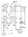
- Figure 1 shows the general block diagram of the invention.
- the system according to the invention makes it possible to carry out a coupling between a microcomputer (or a computer), bearing the reference M0 on this diagram, and one or more measuring devices referenced AM1, AM2, ... AMn.
- the coupling is done by means of interfaces, these interfaces being placed between the access bus 1 of the microcomputer M0 and the access bus of the measuring devices AMn.
- an interface I1 makes it possible to carry out the coupling between the microcomputer M0 and the apparatus AM1
- an interface I2 makes it possible to carry out the same coupling between the microcomputer and the apparatus AM2 ...
- the interface In is used to create the interface between the microcomputer M0 and the device AMn.
- the first bidirectional bus 1 makes it possible to connect the microcomputer to each interface and each interface is connected to a measuring device by the bidirectional bus bearing the reference 2.
- the exchanges between the microcomputer and each of the measuring devices is therefore done by means of buses 1 and 2 via the corresponding interface.
- the microcomputer can address any of the measuring devices via the interface which connects this microcomputer to this measuring device and vice versa.
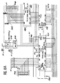
- FIG. 2 shows the general diagram of an interface In, this interface makes it possible to format and transmit information originating from bus 1 to bus 2, and vice versa.
- the wires of bus 1 are connected to a connector J1 and the wires of the bus 2 are connected to a connector J2, these connectors being arranged on the interface card.
- the interface comprises a first circuit 3 making it possible to adapt the electrical level of the input-output lines of the bidirectional bus 1 connected to the connector J1.
- the interface also includes a management circuit 4 for the input-output lines of the bidirectional bus 1 and more specifically of the bidirectional bus 21 for accessing the electrical level adaptation circuit 3.
- the interface also includes a circuit 12 for adapting the electrical levels of the input-output lines of the bidirectional bus 2 and more specifically of the access bus 30 to the connector.
- the input-output lines of bus 2 after adaptation of the electrical levels are divided into three bidirectional buses 24, 25, 26, connected to an input-output line management circuit 11.
- the interface also includes an internal address bus 23, an internal data bus 22 and an internal control bus 27.
- the interface also includes a microprocessor 5, a random access memory 7 of RAM type, a program memory 6, electrically erasable and programmable (EPROM), a time base 10, a clock 9, an address decoding register. 8, a reset and watchdog logic circuit 13 and also a measurement device addressing circuit 14.
- a microprocessor 5 a random access memory 7 of RAM type, a program memory 6, electrically erasable and programmable (EPROM), a time base 10, a clock 9, an address decoding register. 8, a reset and watchdog logic circuit 13 and also a measurement device addressing circuit 14.
- the internal address bus 23 is connected to the input-output line management circuit 11, to the time base circuit 10, to the program memory 6, to the memory 7, to the line management circuit input-output 4, microprocessor 5 and address decoding circuit 8.
- the internal data bus 22 is connected to the two input-output line management circuits 11 and 4, to the two memories 6 and 7, to the time base circuit 10, to the microprocessor 5 and to the device addressing circuit. measurement 14.
- the internal control bus 27 includes a set of control lines on which information is transmitted unidirectionally or bidirectionally between the various elements of the interface card.
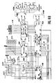
- FIGS. 3a and 3b provide an overview and at the same time detailed of the realization of an interface according to the invention. While retaining an illustrative character, these figures therefore allow the skilled person to implement the invention.
- FIGS. 3a and 3b The various assemblies have been distributed in FIGS. 4, 5, 6, 7, 8A, 8B and 9.
- FIG. 4 represents the diagram of the assemblies J1, 3 and 4 of FIG. 2.
- the terminals B2 to B32 of the connector J1 are connected to the bidirectional bus 1 allowing information to be transmitted between the microcomputer and each interface card.
- wires of this bus referenced 20 inside the card are therefore connected to each of these terminals, a first set of wires constituting a bus 20A is connected to terminals B2 to B9, a second set of wires 20B is connected to terminals B10, 11, 12, 14, 16, 18, 20 and 22, and lines 20C are connected to terminals B13, 15, 17, 19, 21, 23, 24, 31, 32.
- the wires of bus 20C are, either connected to the mechanical ground or to the electrical ground, to the logic ground (at + 5V).
- the assembly 3 is preferably made up of two circuits referenced respectively by 3Z3 and 3Z4 which are circuits for adapting the electrical levels (for example of the SN75 160 A type for one, and SN75 161 A for the other).
- the first bus which consists of 24 lines, was divided into three buses 20A, 20B and 20C, corresponding respectively to data or address lines (bus 20A) to control lines (bus 20B) and to lines of ground or power supply (bus 20C).
- the electrical levels of the bus 20A are adapted by the circuit 3Z3 and the electrical levels of the bus 20B are adapted by the circuit 3Z4.
- the output buses of these two circuits are referenced 21A and 21B.
- the bus 21A therefore consists of 8 lines connected to the output terminals B1 to B8 of the circuit 3Z3.
- the bus 21B is made up of 8 lines connected to the terminals of the exchanges synchronization and control outputs of the 3Z4 circuit.
- the synchronization lines of the exchanges and the control lines correspond to those of a conventional IEEE 488 bus, these lines are lines allowing bidirectional exchanges.
- the information is sequenced by the DAV line which signals that data is available.
- the NDAC line signals that the receiver has not taken the data into account or that the receiver has taken this data into account.
- the NRFD line indicates that one of the devices, either the microcomputer or the measuring device, is not ready to receive data.
- control lines are the ATN line which indicates that the information present on the bus, that is to say the information that will be found on the buses 20A and 21A, is either a functional datum, or an address.
- This line is generally controlled by the bus controller described later.
- the IFC line is used to initialize the interface, the signal transmitted by this line generally being generated by the bus controller, in this case MO.
- the REN line is used to signal the remote control being taken by the bus controller.
- the M0 computer can only communicate with the interface when it has sent a required status signal on this line.
- the EOI line fulfills two functions: an end of transmission function, an identification function.
- the status transmitted by the line is positioned by the transmitter to physically signal the end of a message, the operation of this line can be programmed to choose whether or not to activate it.
- the second role is the identification role which, by positioning the required state on this line, recognizes the requester of the interruption.
- the SRQ line is used to transmit the interrupt request.
- the other lines constituting the bus 20C are assigned to shields, logic ground, mechanical ground, shielding of lines for synchronization of the exchanges.
- the connector J1 constitutes so part of the connector used to connect the microcomputer M0 to the interface cards I1 .... In.
- FIG 4 there is also shown the assembly 4 which performs the function of line management controller.
- this management controller is produced by a micro-processor of the MUPD72 10 type.
- This management controller in fact makes it possible to free the main microprocessor designated by the reference 5, from all the digital filtering sequencing tasks while remaining transparent to this main processor.
- the circuit 4 will in fact make a request to the main processor only on error conditions which it cannot itself resolve.
- the lines of the bus 21A are connected to the terminals DI01 to DI08 of circuit 4.
- the lines of the bus 21B are connected to the terminals IFC up to SRQ as can be seen in FIG. 4.
- the circuit therefore delivers information to these output terminals D0 to D7 on a parallel bus 22 which corresponds to an internal data bus for the interface, but which can, as has already been said, transmit information which are either addresses , or functional data.
- the circuit also uses information on its input terminals RS0 to RS2 which are 3 addressing bits A0, A1, A2 from the microprocessor 5.
- This circuit 4 also uses write and read orders at its terminals WR and RD.
- Circuit 4 also includes a reset terminal RES and a terminal for the clock signal CLK.
- FIG. 5 the assemblies 5, 6 and 7 are shown.
- the interface is built around processor 5, which is of the Z80 CMOS type, clocked with a 4 MHz clock.
- the interface program is contained in the 8 kbyte EPROM memory bearing the reference 6, which is a D27C64 or ⁇ P D27C64 type circuit.
- the various messages and variables are stored in the RAM memory bearing the reference 7 of 8 Kbytes of CMOS technology of the ⁇ PD43 64 type.
- the internal bus 22 is connected to the data inputs D0 to D7 of circuit 5, to the data inputs D0 to D7 of the memory 7 and to the data inputs D0 to D7 of the EPROM memory 6.
- the internal bus 23 is connected to the inputs address A0, A15 of the microprocessor 5 to the address inputs A0, A12 of the RAM memory 7 and to the address inputs A0, A12 of the EPROM memory 6.
- the RAM memory allows messages to be stored by a stack system; it is used to prepare the structure of control messages. This memory also contains the status words.
- the microprocessor Upon detection of the presence of a message in reception, the microprocessor will search the stack for the number of characters relating to the transmitted frame and will transfer them to the working area of the RAM memory.
- the ST3 strap makes it possible to replace the EPROM 6 memory with a compatible RAM memory for maintenance or development needs.
- FIG. 6 represents the assemblies 13 and 9.
- the assembly 13 constitutes a logic reset and watchdog circuit and the assembly 9 performs the clock function of the microprocessor 5 and of the line management controller 4. This clock generates a 4 MHz frequency signal.
- the oscillator placed in the clock starts as soon as the interface is powered up.
- the 13Z5 circuit performs the watchdog function.
- it is a circuit of the 74HC423A type.
- the watchdog allows the microprocessor 5 to run in an application and, as soon as an external execution fault occurs, to reset the entire system in hardware.
- the watchdog therefore generates the RESET reset signal of the interface and of the microprocessor 5 of this interface.
- This 13Z5 circuit is a double monostable, half of a circuit used to widen the slots of the initialization signal and the other half is triggered when the power is turned on: it must be kept under control of the memory program 7 In the absence of maintenance, which corresponds to a stable state, the circuit therefore generates the interface reset signal.
- a programmable logic circuit of the PAL C16L8 type is used to solve the reset problems when the interface is powered up.
- the computer can send this command by the line which is connected to the IFC terminal of circuit 13Z10.
- This line therefore makes it possible to arm the watchdog independently of the microprocessor 5 by means of this programmable logic circuit 13Z10.
- the watchdog 13Z5 is put in an unstable position and is kept there when the power is turned on.
- the microprocessor 5 has the possibility of rearming this dog or not to rearm it.
- the ARMWD line is used to rearm the watchdog during writes to a reserved address.
- the watchdog When the watchdog is not rearmed, its output levels drop down and position the inputs of the PAL13Z10 circuit so that this circuit sends an initialization signal to the whole system.
- the assemblies 8 and 10 are shown.
- the assembly 8 is an address decoding circuit.
- Set 10 is the time base circuit.
- the address decoding circuit 8 makes it possible to generate the addresses of the memory plane and of the peripheral circuits initialized when the interface is powered up. This address decoding circuit generates validations for the input-output line management means formed by the assembly 11.
- This circuit 8 is connected to the internal address bus 23. It is also connected to the reset line, to the microprocessor by control lines, to the memory write lines 6, 7 and to the command line of writing memory 6. It generates the reset signal for the watchdog.
- the time base circuit 10 is connected on the one hand to the internal bus 22, on the other hand to the internal bus 23. This circuit 10 is also connected to certain output terminals of the address decoding circuit 8. It receives the RESET reset signal. It also receives the CLK clock signal.
- FIG. 8A represents the diagram of the assemblies 11A and 12A.
- FIG. 8B represents the diagram of the assemblies 11B, 12B.
- the assembly 11 comprises three peripheral circuits of the TMPZ 84C20P type connected to the internal address bus 23 and to the internal data bus 22. This assembly 11 constitutes a circuit for managing the input-output lines on the measuring device side.
- the three input-output peripherals bear the references 111, 112, 113 and can be addressed by the microprocessor 5 by means of two address bits on the address inputs A0, A1.
- the three circuits 111, 112, 113 are also connected to the initialization line, to the interrupt request line INT, to the line of the clock signal CLK, to the address decoding circuit 8.
- interface circuits 111, 112, 113 are also connected to the bidirectional bus 2 for access to the measuring devices, and this by means of an electrical level adaptation circuit bearing the reference 12.
- This circuit 12 consists of two adapter circuits of the 74LS245 type, of an adapter circuit of the 74LS244 type. It also includes a programmable logic circuit PALC16L8 bearing the reference 124.
- the programmable logic circuits which are used in the interface in fact each form part of the same circuit.
- FIG. 9 represents the diagram of the assembly J2, that is to say of the part of the connector which allows the connection between the bidirectional bus 2 and the interface.
- This bidirectional bus 2 is a 16-bit parallel bus.
- the bus comprises 16 bidirectional open collector type data lines which are therefore connected to a resistor network R11 and R12. These 16 lines bear the references 30A and 30B.
- the lines of the bus 30A are connected to the address inputs of the electrical level adaptation circuit bearing the reference 121.
- the other eight data lines constitute the bidirectional bus 30B connected to the address inputs of the circuit 122.
- This bus 2 also includes a DSNT line which indicates that the transmitter module has positioned data on the bus (data sent). The receiving interface then positions a DRCV line (data received) and vice-versa.
- the bus 30C comprises 8 bus control lines, a busy bus line CBBZY which is positioned by the bus controller 11, and more precisely by the circuit 111 via the circuits Z10 and Z15.
- the bus 30C also includes a CLI line indicating to the interface that an interrupt request is taken into account.
- the encoding of the measuring device connected to the interface is made from three lines BS1, BS2, BS3 and two lines BQ1, BQ2 are reserved for the description of the direction of information transfer.
- the other lines are either connected to a mechanical ground, or to an electrical ground, or to the shield.
- the electrical level adapter circuits are circuits with three-state logic, positioned in the high impedance state on initialization of the measuring device and of the interface. These circuits are TTL circuits.
- the 74LS245 circuit is a bidirectional bus driver for the data bus, the 74LS244 circuit is a unidirectional driver for the control signals.
- Port B of PI0 113 is only programmed at the output to manage the control lines.
- the PIO 112 manages the DSNT and DRCV synchronization lines on transmission by means of the driver circuit Z15 (of the 74LS241 type) which is made bidirectional by a set of connections external to the box.
- this Z15 driver circuit is always positioned at the input to listen to what is coming from the measuring device.
- the port B of this circuit PI0 112 also makes it possible to manage the setting in high impedance by the ports B2 to B4 of the adaptation circuits of an electrical level Z15, 123, 121 and 122. It also makes it possible to validate the bus of the circuit 123 through its port B4. It validates circuits 121 and 122 when transmitting data or receiving.
- Port B of PI0 111 is programmed for reading. Its lines are connected to a network of resistors R10 and allow the coding of the address of the interface.
- Port A of PI0 111 has two lines (A1, A2) for reading incoming information and a line connected to circuit Z10.
- This circuit Z10 makes it possible to detect the request for an interruption originating from a measuring device.
- the driver circuit Z15 which is part of the same housing, is connected to this circuit Z11 and is in a high impedance state at power-up, which inhibits the interrupt function during the initialization of the interface by forcing states to an inactive level using resistors R7.
- a logic circuit 124 makes it possible to choose the direction of operation of the reads / writes of the circuits 121, 122, 123. It in fact makes it possible to carry out a direction command.
Landscapes
- Engineering & Computer Science (AREA)
- Theoretical Computer Science (AREA)
- Physics & Mathematics (AREA)
- General Engineering & Computer Science (AREA)
- General Physics & Mathematics (AREA)
- Debugging And Monitoring (AREA)
Applications Claiming Priority (2)
| Application Number | Priority Date | Filing Date | Title |
|---|---|---|---|
| FR8908203A FR2648588A1 (fr) | 1989-06-20 | 1989-06-20 | Systeme de couplage avec interface entre au moins deux appareils electroniques ayant des bus d'acces de format different |
| FR8908203 | 1989-06-20 |
Publications (1)
| Publication Number | Publication Date |
|---|---|
| EP0404653A1 true EP0404653A1 (de) | 1990-12-27 |
Family
ID=9382946
Family Applications (1)
| Application Number | Title | Priority Date | Filing Date |
|---|---|---|---|
| EP90401701A Withdrawn EP0404653A1 (de) | 1989-06-20 | 1990-06-18 | Kopplungssystem mit einer Schnittstelle zwischen mindestens zwei elektronischen Geräten mit verschiedenen Formatzugriffbussen |
Country Status (2)
| Country | Link |
|---|---|
| EP (1) | EP0404653A1 (de) |
| FR (1) | FR2648588A1 (de) |
Cited By (1)
| Publication number | Priority date | Publication date | Assignee | Title |
|---|---|---|---|---|
| KR100394246B1 (ko) * | 2000-08-29 | 2003-08-09 | 바이코시스템 주식회사 | 자동제어용 디지탈 신호처리장치 및 그 인터페이스 방법 |
Citations (3)
| Publication number | Priority date | Publication date | Assignee | Title |
|---|---|---|---|---|
| EP0068992A2 (de) * | 1981-06-18 | 1983-01-05 | The Bendix Corporation | Verknüpfte Datensysteme |
| WO1984001447A1 (en) * | 1982-09-30 | 1984-04-12 | Burroughs Corp | Line support processor for data transfer system |
| EP0273136A2 (de) * | 1986-10-31 | 1988-07-06 | Honeywell Bull Inc. | Universelles Peripheriesteuerungsmodul mit Konfigurationsladung während der Initialisierung |
-
1989
- 1989-06-20 FR FR8908203A patent/FR2648588A1/fr not_active Withdrawn
-
1990
- 1990-06-18 EP EP90401701A patent/EP0404653A1/de not_active Withdrawn
Patent Citations (3)
| Publication number | Priority date | Publication date | Assignee | Title |
|---|---|---|---|---|
| EP0068992A2 (de) * | 1981-06-18 | 1983-01-05 | The Bendix Corporation | Verknüpfte Datensysteme |
| WO1984001447A1 (en) * | 1982-09-30 | 1984-04-12 | Burroughs Corp | Line support processor for data transfer system |
| EP0273136A2 (de) * | 1986-10-31 | 1988-07-06 | Honeywell Bull Inc. | Universelles Peripheriesteuerungsmodul mit Konfigurationsladung während der Initialisierung |
Non-Patent Citations (3)
| Title |
|---|
| ASILOMAR CONFERENCE ON CIRCUITS SYSTEM AND COMPUTERS 7 novembre 1977, Pacific Grove, California, US; pages 477 - 480; T. Nishimukai et al.: "Universal IO device controller by using programmable logic arrays (PLA)" * |
| IEEE TRANSACTIONS ON INDUSTRIAL ELECTRONICS AND CONTROL vol. 26, no. 3, août 1979, NEW YORK US pages 151 - 155; C.J. Tavora: "The remote link unit - an advanced remote terminal concept" * |
| PATENT ABSTRACTS OF JAPAN vol. 9, no. 69 (E-305)(1792) 29 mars 1985, & JP-A-59 205857 (YASUSHI SUZUKI) 21 novembre 1984, * |
Cited By (1)
| Publication number | Priority date | Publication date | Assignee | Title |
|---|---|---|---|---|
| KR100394246B1 (ko) * | 2000-08-29 | 2003-08-09 | 바이코시스템 주식회사 | 자동제어용 디지탈 신호처리장치 및 그 인터페이스 방법 |
Also Published As
| Publication number | Publication date |
|---|---|
| FR2648588A1 (fr) | 1990-12-21 |
Similar Documents
| Publication | Publication Date | Title |
|---|---|---|
| EP0461971B1 (de) | Elektronische Verbindungsvorrichtung | |
| EP0394114B1 (de) | Multifunktionskoppler zwischen einer zentralen Verarbeitungseinheit eines Rechners und verschiedenen Peripheriegeräten dieses Rechners | |
| EP0012886B1 (de) | Eingabe/Ausgabe-Steuereinheit für ein Datenverarbeitungssystem | |
| EP0649547A1 (de) | Massenspeicherkarte mit eingangs- ausgangsfunktion. | |
| EP0272969B1 (de) | Verfahren und programmierbare Vorrichtung zur Umkodierung von Zeichenketten | |
| FR2612313A1 (fr) | Selecteur programmable d'options | |
| FR2862147A1 (fr) | Reconfiguration dynamique de liaisons de type pci-express | |
| FR2479534A1 (fr) | Circuit de detection d'erreur pour une memoire | |
| EP0755010A1 (de) | Schnittstelleneinrichtung zwischen einem Rechner redundanter Architektur und einem Kommunikationsmittel | |
| EP1072024A1 (de) | Verfahren zum umschalten von anwendungen in einer chipkarte für mehrere anwendungen | |
| EP0395469A2 (de) | Tragbarer Mikrorechner | |
| EP0182678B1 (de) | Fernverarbeitungsterminal mit externen Anschlüssen | |
| EP0698851A1 (de) | Speicher-/Chipkartenlesersystem | |
| FR2493562A1 (fr) | Systeme d'utilisation de disques en commun et d'intercommunication entre disques | |
| EP0404653A1 (de) | Kopplungssystem mit einer Schnittstelle zwischen mindestens zwei elektronischen Geräten mit verschiedenen Formatzugriffbussen | |
| EP0983553B1 (de) | Speicherplattenuntersystem mit kofigurierbaren mehrfachschnittstellen | |
| EP0589743B1 (de) | Modulare Vorrichtung zum Koppeln und zum Multiplexen von unterschiedlichen Bussen | |
| EP0441707B1 (de) | Koppler für Serienbus | |
| WO1994021074A1 (fr) | Systeme de communication avec un reseau | |
| EP1051693B1 (de) | Asynchrone speicherkarte | |
| FR2724470A1 (fr) | Procede et carte electronique pour emuler une memoire a bande magnetique | |
| EP0297964A1 (de) | Verfahren zur Steuerung von Vorrichtungen durch ein lokales Netzwerk, insbesondere zur Automatisierung einer Werkstatt | |
| EP0459877A1 (de) | Rechensystem zur Datenübertragung im Stossbetrieb | |
| FR2604003A1 (fr) | Systeme d'interconnexion d'ordinateurs identiques ou compatibles | |
| FR2662522A1 (fr) | Dispositif informatique de transfert de donnees en mode rafale. |
Legal Events
| Date | Code | Title | Description |
|---|---|---|---|
| PUAI | Public reference made under article 153(3) epc to a published international application that has entered the european phase |
Free format text: ORIGINAL CODE: 0009012 |
|
| AK | Designated contracting states |
Kind code of ref document: A1 Designated state(s): DE GB |
|
| 17P | Request for examination filed |
Effective date: 19910531 |
|
| STAA | Information on the status of an ep patent application or granted ep patent |
Free format text: STATUS: THE APPLICATION IS DEEMED TO BE WITHDRAWN |
|
| 18D | Application deemed to be withdrawn |
Effective date: 19940104 |