EP0405577A2 - Schaltung für Rahmenumwandlung - Google Patents
Schaltung für Rahmenumwandlung Download PDFInfo
- Publication number
- EP0405577A2 EP0405577A2 EP90112453A EP90112453A EP0405577A2 EP 0405577 A2 EP0405577 A2 EP 0405577A2 EP 90112453 A EP90112453 A EP 90112453A EP 90112453 A EP90112453 A EP 90112453A EP 0405577 A2 EP0405577 A2 EP 0405577A2
- Authority
- EP
- European Patent Office
- Prior art keywords
- data
- memory
- address
- conversion circuit
- signal
- Prior art date
- Legal status (The legal status is an assumption and is not a legal conclusion. Google has not performed a legal analysis and makes no representation as to the accuracy of the status listed.)
- Ceased
Links
Images


Classifications
-
- H—ELECTRICITY
- H04—ELECTRIC COMMUNICATION TECHNIQUE
- H04L—TRANSMISSION OF DIGITAL INFORMATION, e.g. TELEGRAPHIC COMMUNICATION
- H04L25/00—Baseband systems
- H04L25/02—Details ; arrangements for supplying electrical power along data transmission lines
- H04L25/05—Electric or magnetic storage of signals before transmitting or retransmitting for changing the transmission rate
Definitions
- the present invention relates to a frame conversion circuit for demultiplexing incoming various multiplexed signals that have been transmitted over a high-speed communication line, on the receiving side, and then converting the separated signals into the same frames thereby unifying the speeds of the various data signals.
- a multiplexer In digital transmission systems, in general, several pieces of information are transmitted after being multiplexed in order to achieve effective use of the transmission medium and greater economy in the transmission. Such multiplexing is performed on the time base, and one period of the multiplexed signal is called a frame and the multiplexing method is called the time-division multiplexing.
- a plurality of low order group digital signals are time-divisionally multiplexed by a multiplexer into high order group digital signals, whereby a greater number of channels are made possible to be transmitted over the same link.
- These signals are transmitted from one exchange to another by a suitable transmission means capable of accommodating the necessary number of channels, and thereby transmitted to a destination.
- the high order digital signal is separated into low order group digital signals by a demultiplexer.
- ISDN Integrated Services Digital Network
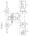
- FIG. 1 and FIG. 2 A representative example of prior art frame conversion circuits will be described below with reference to FIG. 1 and FIG. 2.
- the tristate buffer 12 and a tristate buffer 16 are enabled and, simultaneously, address signals arranged at random (3, 1, and 4 in FIG. 2) for indicating addresses at which the data should be written into a memory 1 are output from a write address generator 14.
- the data are written into the memory according to these address signals.
- the random address signals are adapted to be different according to the kinds of data.
- a tristate buffer 17 is enabled and, at the same time, sequential address signals (1, 2, 3, 4, 5, 6 in FIG.
- a sign bit adding/checking portion 8 is formed of such parts as a cyclic redundancy check. It adds sign bits to the rearmost position of the data written in the memory, and at the time of reading of the data, it monitors the sign bits thereby checking whether the data is properly transmitted and received. By repeating such random writing of data into the memory according to the kinds of data and sequential reading of the data from the memory, the frame conversion for arranging various data of different speeds into unified high speed signals is performed.
- an object of the present invention is to provide a frame conversion circuit in which no error will be produced in the step of sign bit check.
- Another object of the present invention is to provide a highly reliable frame conversion circuit in which such data as to cause erroneous synchronization will not be included in the read out data.
- a frame conversion circuit including write address generation means for generating a random address signal for writing an incoming transmitted data signal into a memory, means fur adding sign bits to the data to be written into the memory and checking the sign bits at the time when the data is read out, and read address generation means for generating a sequential address signal for reading the data from the memory, characterized by initial value input means for writing an arbitrary initial value into the memory at each address each time the data is read out of the memory sequentially from the first address according to the read address signal.
- the initial value input means is formed of plural pull-up resistors connected in parallel with plural output lines of a tristate buffer to which the transmitted signal is input.
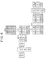
- the frame conversion circuit of the present invention differs from the prior art frame conversion circuit only in that it is provided with an initial value inputting circuit 19 and otherwise quite the same as the prior art circuit.
- the initial value inputting circuit 19 is adapted, each time data is read out sequentially from each address of a memory according to a read address signal, to write an arbitrary initial value into the memory at the address from which the data is read out.
- the initial value is preferably formed "all 1s" or "all 0s. Since, such an initial value is written, each time data is readout, into the memory at the address from which the data is read out, an error does not occur at a sign bit check and erroneous synchronization is also prevented from occurring.
- the frame conversion circuit of the present embodiment is, for example, of a 24-multiframe structure in an octet multiplexing method with one frame being of a length of an octet and, hence, output lines of the tristate buffer 12 are formed of eight lines.
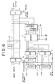
- the write address generator 14 in FIG. 5 is formed of a counter 22 and a ROM 21 and the read address generator is formed of a counter 20.
- the ROM 21 there are stored write addresses corresponding to the kinds of data such as general data and speech data to be written into the memory 11, and it is adapted such that the patterns of the address signal generated therefrom are switched by a switching signal generated by a controller, not shown, according to the kind of data to be written into the memory 11.
- the address signals are output in the order of 3, 2, 6 in binary numbers, whereas, in the case of speech data, the address signals are output in the order of 4, 1, 6. More specifically, the output from the ROM 21 becomes different even when the signal from the counter is the same. For example, when the output of the counter 22 is 1, the address signal becomes 3 if the data written into the memory 11 is general data, whereas it becomes 4 if the data is speech data.
- the read counter 20 outputs the count value in a binary number to the memory 11.
- the counter 22 is reset each time data is read out from the memory 11, while the counter 20 is reset each time data is written into the memory 11.
- the tristate buffers 12, 16, and 17 are adapted such that their plural internal transistors are controlled by control signals (R/W signals) from the controller, not shown, so that they are brought into enable state or disable state.
- a parity code is added to the input data output from the tristate buffer 12 by the parity adding/checking circuit 18 and the input data with the parity code attached thereto are written into the memory 11 according to the address signals from the ROM 21 (3, 1, and 4 in FIG. 7) and a write enable signal. After the described operations are repeated several times, the data A, B, and C are written into the memory at the designated addresses.
- the tristate buffer 17 Upon completion of the writing of data into the memory 11, the tristate buffer 17 is brought into an enable state, and the count values of the counter 20 are output in binary numbers to the memory 11. Since these counted values become the read address signals as they are (1, 2, 3, 4, 5, and 6 in FIG. 7), data are read out from the memory 11 sequentially according to these read address signals and an output enable signal. At this time, a parity check is simultaneously performed by the parity adding/checking circuit 18. The read out data are once latched by the flip-flop circuit 13 according to a latch timing signal and, then, are output therefrom.
- the initial value inputting circuit 19 is formed of pull-up resistors connected in parallel with the eight output lines of the tristate buffer 12, and when, the output of the tristate buffer 12 is in the high impedance state (R/W signal is low), the output lines are held High. Therefore, the initial values input by the initial value inputting circuit 19 in the present embodiment become "all 1s".
Landscapes
- Engineering & Computer Science (AREA)
- Power Engineering (AREA)
- Computer Networks & Wireless Communication (AREA)
- Signal Processing (AREA)
- Time-Division Multiplex Systems (AREA)
Applications Claiming Priority (2)
| Application Number | Priority Date | Filing Date | Title |
|---|---|---|---|
| JP1167840A JPH0331928A (ja) | 1989-06-29 | 1989-06-29 | フレーム変換回路 |
| JP167840/89 | 1989-06-29 |
Publications (2)
| Publication Number | Publication Date |
|---|---|
| EP0405577A2 true EP0405577A2 (de) | 1991-01-02 |
| EP0405577A3 EP0405577A3 (en) | 1991-09-18 |
Family
ID=15857055
Family Applications (1)
| Application Number | Title | Priority Date | Filing Date |
|---|---|---|---|
| EP19900112453 Ceased EP0405577A3 (en) | 1989-06-29 | 1990-06-29 | Frame conversion circuit |
Country Status (4)
| Country | Link |
|---|---|
| US (1) | US5341492A (de) |
| EP (1) | EP0405577A3 (de) |
| JP (1) | JPH0331928A (de) |
| CA (1) | CA2020015A1 (de) |
Families Citing this family (12)
| Publication number | Priority date | Publication date | Assignee | Title |
|---|---|---|---|---|
| DE4216559C2 (de) * | 1992-05-20 | 1995-05-24 | Freudenberg Carl Fa | Schwenklager |
| GB2269077A (en) * | 1992-07-22 | 1994-01-26 | Ibm | Conversion of ISDN LAPB and LAPD frames |
| US5534937A (en) * | 1994-04-14 | 1996-07-09 | Motorola, Inc. | Minimum-delay jitter smoothing device and method for packet video communications |
| WO2004097840A1 (ja) * | 1995-09-06 | 2004-11-11 | Osamu Yamada | Sdram用テストパターン発生装置及び方法 |
| JPH11103415A (ja) | 1997-09-26 | 1999-04-13 | Marantz Japan Inc | フレーム変換装置 |
| US6317160B1 (en) | 1997-11-28 | 2001-11-13 | U.S. Philips Corporation | Frame conversion for asynchronous input image signals |
| JPH11164202A (ja) * | 1997-11-28 | 1999-06-18 | Marantz Japan Inc | フレーム変換装置 |
| US7219173B2 (en) * | 2001-07-31 | 2007-05-15 | Micronas Usa, Inc. | System for video processing control and scheduling wherein commands are unaffected by signal interrupts and schedule commands are transmitted at precise time |
| US7184101B2 (en) * | 2001-07-31 | 2007-02-27 | Micronas Usa, Inc. | Address generation for video processing |
| US7142251B2 (en) * | 2001-07-31 | 2006-11-28 | Micronas Usa, Inc. | Video input processor in multi-format video compression system |
| US7085320B2 (en) * | 2001-07-31 | 2006-08-01 | Wis Technologies, Inc. | Multiple format video compression |
| US20050207663A1 (en) * | 2001-07-31 | 2005-09-22 | Weimin Zeng | Searching method and system for best matching motion vector |
Family Cites Families (5)
| Publication number | Priority date | Publication date | Assignee | Title |
|---|---|---|---|---|
| US4186379A (en) * | 1977-04-28 | 1980-01-29 | Hewlett-Packard Company | High-speed data transfer apparatus |
| JPS5471530A (en) * | 1977-11-18 | 1979-06-08 | Hitachi Denshi Ltd | Ic memory clear circuit |
| US4485435A (en) * | 1981-03-09 | 1984-11-27 | General Signal Corporation | Memory management method and apparatus for initializing and/or clearing R/W storage areas |
| US4873684A (en) * | 1985-05-29 | 1989-10-10 | Trio Kabushiki Kaisha | Method and apparatus for multiplexing of input signals having differing frequencies and demultiplexing same |
| US4740971A (en) * | 1986-02-28 | 1988-04-26 | Advanced Micro Devices, Inc. | Tag buffer with testing capability |
-
1989
- 1989-06-29 JP JP1167840A patent/JPH0331928A/ja active Pending
-
1990
- 1990-06-27 CA CA002020015A patent/CA2020015A1/en not_active Abandoned
- 1990-06-29 EP EP19900112453 patent/EP0405577A3/en not_active Ceased
-
1993
- 1993-11-19 US US08/155,159 patent/US5341492A/en not_active Expired - Fee Related
Also Published As
| Publication number | Publication date |
|---|---|
| CA2020015A1 (en) | 1990-12-30 |
| JPH0331928A (ja) | 1991-02-12 |
| US5341492A (en) | 1994-08-23 |
| EP0405577A3 (en) | 1991-09-18 |
Similar Documents
| Publication | Publication Date | Title |
|---|---|---|
| US5781129A (en) | Adaptive encoder circuit for multiple data channels and method of encoding | |
| US8165257B2 (en) | Methods and apparatus for interface buffer management and clock compensation in data transfers | |
| EP0405577A2 (de) | Schaltung für Rahmenumwandlung | |
| EP0378122A1 (de) | Parallele Zeitstufen-Matrix und Schaltblockmodul zur Anwendung in dieser Matrix | |
| EP0334357B1 (de) | Impulseinblendungsanordnung | |
| JPH02226926A (ja) | 多重チャネルpcmタイプのリング上にhdlcフレームを伝送するためのシステム | |
| JPH02226943A (ja) | ハイレベルデータリンク制御手順フレームを解析し且つ処理するためのシステム | |
| KR920005216B1 (ko) | 저장 프로그램 제어식 통신시스템 및 그 작동방법 | |
| EP0323222A2 (de) | Sende- und Empfangssystem eines HDLC-Datenrahmens über einen Zeitmultiplexübertragungsweg | |
| JPH098781A (ja) | 伝送速度変換装置 | |
| US6208648B1 (en) | Network element and input/output device for a synchronous transmission system | |
| US6330237B1 (en) | Time slot assignment circuit | |
| US5444658A (en) | Elastic store memory circuit | |
| JPH0267848A (ja) | 可変長データフレームの転送方式 | |
| US5425062A (en) | Serial rate conversion circuit with jitter tolerant payload | |
| JP2702171B2 (ja) | フレーム変換回路 | |
| JPH07123247B2 (ja) | デイジタルデ−タ伝送方法 | |
| JP2511050B2 (ja) | 多重伝送回路の加入者線終端装置 | |
| JPH1093536A (ja) | 伝送装置のユニット間インタフェース方式 | |
| JPS6141186B2 (de) | ||
| KR100228381B1 (ko) | 티유12 및 티유11 신호가 혼재된 종속신호를 스위칭하는 공간 스위칭 장치 | |
| JP3730379B2 (ja) | 通信回線データを端末へ出力する装置 | |
| KR100421951B1 (ko) | 전송시스템의 병렬 브이씨3 매핑회로 | |
| JP3010634B2 (ja) | フレーム同期多重処理方式 | |
| JP3868047B2 (ja) | バッファ回路 |
Legal Events
| Date | Code | Title | Description |
|---|---|---|---|
| PUAI | Public reference made under article 153(3) epc to a published international application that has entered the european phase |
Free format text: ORIGINAL CODE: 0009012 |
|
| AK | Designated contracting states |
Kind code of ref document: A2 Designated state(s): DE FR GB |
|
| PUAL | Search report despatched |
Free format text: ORIGINAL CODE: 0009013 |
|
| AK | Designated contracting states |
Kind code of ref document: A3 Designated state(s): DE FR GB |
|
| RHK1 | Main classification (correction) |
Ipc: H04J 3/16 |
|
| 17P | Request for examination filed |
Effective date: 19911008 |
|
| 17Q | First examination report despatched |
Effective date: 19940125 |
|
| GRAG | Despatch of communication of intention to grant |
Free format text: ORIGINAL CODE: EPIDOS AGRA |
|
| STAA | Information on the status of an ep patent application or granted ep patent |
Free format text: STATUS: THE APPLICATION HAS BEEN REFUSED |
|
| 18R | Application refused |
Effective date: 19961108 |