EP0406366B1 - Programmierbarer hochgeschwindigkeitsteiler - Google Patents
Programmierbarer hochgeschwindigkeitsteiler Download PDFInfo
- Publication number
- EP0406366B1 EP0406366B1 EP90900469A EP90900469A EP0406366B1 EP 0406366 B1 EP0406366 B1 EP 0406366B1 EP 90900469 A EP90900469 A EP 90900469A EP 90900469 A EP90900469 A EP 90900469A EP 0406366 B1 EP0406366 B1 EP 0406366B1
- Authority
- EP
- European Patent Office
- Prior art keywords
- output
- input
- coupled
- counter
- prescaler
- Prior art date
- Legal status (The legal status is an assumption and is not a legal conclusion. Google has not performed a legal analysis and makes no representation as to the accuracy of the status listed.)
- Expired - Lifetime
Links
- 230000000295 complement effect Effects 0.000 claims description 11
- 230000003111 delayed effect Effects 0.000 claims description 11
- 230000007704 transition Effects 0.000 claims description 11
- 230000002401 inhibitory effect Effects 0.000 claims description 2
- 230000004044 response Effects 0.000 claims description 2
- 230000006870 function Effects 0.000 abstract description 9
- 238000010586 diagram Methods 0.000 description 19
- 238000013459 approach Methods 0.000 description 7
- 230000000630 rising effect Effects 0.000 description 3
- 230000008901 benefit Effects 0.000 description 2
- 230000008859 change Effects 0.000 description 2
- 230000001934 delay Effects 0.000 description 2
- 238000000034 method Methods 0.000 description 2
- 230000003068 static effect Effects 0.000 description 2
- 230000001629 suppression Effects 0.000 description 2
- 238000010276 construction Methods 0.000 description 1
- 230000008878 coupling Effects 0.000 description 1
- 238000010168 coupling process Methods 0.000 description 1
- 238000005859 coupling reaction Methods 0.000 description 1
- 230000002939 deleterious effect Effects 0.000 description 1
- 230000009977 dual effect Effects 0.000 description 1
- 230000000694 effects Effects 0.000 description 1
- 238000005516 engineering process Methods 0.000 description 1
- 230000004048 modification Effects 0.000 description 1
- 238000012986 modification Methods 0.000 description 1
- 230000008569 process Effects 0.000 description 1
- 238000001228 spectrum Methods 0.000 description 1
Images


Classifications
-
- H—ELECTRICITY
- H03—ELECTRONIC CIRCUITRY
- H03K—PULSE TECHNIQUE
- H03K23/00—Pulse counters comprising counting chains; Frequency dividers comprising counting chains
- H03K23/64—Pulse counters comprising counting chains; Frequency dividers comprising counting chains with a base or radix other than a power of two
- H03K23/66—Pulse counters comprising counting chains; Frequency dividers comprising counting chains with a base or radix other than a power of two with a variable counting base, e.g. by presetting or by adding or suppressing pulses
- H03K23/665—Pulse counters comprising counting chains; Frequency dividers comprising counting chains with a base or radix other than a power of two with a variable counting base, e.g. by presetting or by adding or suppressing pulses by presetting
-
- H—ELECTRICITY
- H03—ELECTRONIC CIRCUITRY
- H03K—PULSE TECHNIQUE
- H03K21/00—Details of pulse counters or frequency dividers
- H03K21/08—Output circuits
- H03K21/10—Output circuits comprising logic circuits
-
- H—ELECTRICITY
- H03—ELECTRONIC CIRCUITRY
- H03K—PULSE TECHNIQUE
- H03K23/00—Pulse counters comprising counting chains; Frequency dividers comprising counting chains
- H03K23/64—Pulse counters comprising counting chains; Frequency dividers comprising counting chains with a base or radix other than a power of two
- H03K23/66—Pulse counters comprising counting chains; Frequency dividers comprising counting chains with a base or radix other than a power of two with a variable counting base, e.g. by presetting or by adding or suppressing pulses
- H03K23/667—Pulse counters comprising counting chains; Frequency dividers comprising counting chains with a base or radix other than a power of two with a variable counting base, e.g. by presetting or by adding or suppressing pulses by switching the base during a counting cycle
-
- H—ELECTRICITY
- H03—ELECTRONIC CIRCUITRY
- H03K—PULSE TECHNIQUE
- H03K23/00—Pulse counters comprising counting chains; Frequency dividers comprising counting chains
- H03K23/64—Pulse counters comprising counting chains; Frequency dividers comprising counting chains with a base or radix other than a power of two
- H03K23/68—Pulse counters comprising counting chains; Frequency dividers comprising counting chains with a base or radix other than a power of two with a base which is a non-integer
Definitions
- the invention relates generally to programmable dividing or counting circuitry. More specifically, the invention concerns high speed frequency dividers usable in such applications as phase-lock-loop frequency synthesizers or precision timers.
- a programmable divider Two desirable properties of a programmable divider are that it operate at a high clock rate and that its division modulus be programmable in the smallest possible steps (integer steps are usually desired).
- at least some of the circuitry containing the logic gates required for the divider to be programmable is clocked at the input frequency of the programmable divider, which limits the maximum clock frequency that can be used. This is due to the fact that the logic gates employed have inherent delays which in turn limit the maximum external clock frequency able to be used. Higher input frequencies are accommodated by using a divide-by-P fixed-modulus prescaler (where P is commonly 2 or 4) in a stage prior to the programmable divider.
- the fixed-modulus prescaler can run at a higher speed, since it need only contain latches with no logic gates between the latches.
- the prescaler normally supplies one clock pulse to the programmable divider for every N clock pulses presented to the prescaler input.
- This conventional combination of a prescaler and a programmable divider reduces the possible division moduli to those that are integer multiples of the prescaler modulus N.
- the fundamental limitation of this conventional arrangement is that, each time the prescaler is driven through its internal cycle by N input clock pulses, only one internal transition of the prescaler wave form is used to clock the subsequently operating programmable divider. The timing information which exists in the remaining N-1 input pulses is not utilized in any way in the conventional approach, but is ignored, and therefore lost.
- non-integer division may be effected by alternating between N and N+1 in such a way as to provide an average count which is some desired fraction with a value between N and N+1.
- obtaining a divisor of N+a/b by dividing by N for "a" times and N+1 for (b-a) times produces an output with subharmonics down to 1/b of the output frequency.
- EP-A-0280126 describes a programmable frequency divider which includes a flip-flop to selectively add a unit amount to the divisor data sent to an initial divider stage. The output from the initial divider stage is further divided by a second divider stage to clock the flip-flop. Comparator logic responsive to fractional bits of the divisor data and to respective outputs from the second divider is used to control the resetting of the flip-flop.
- US Patent No. 4623846 describes a clock generator including a programmable divider and prescaler which accept a rate signal and a master clock signal. A constant duty cycle characteristic of the clock signal is obtained regardless of the output clock signal's frequency. A memory element which generates the output signal is placed in one logical state when a counter portion of the divider reaches a terminal count. The memory element is placed in an opposing logical state whenever the counter achieves a half of its programmed value. A duty cycle compensator uses information contained in the least significant bit of the divisor value to modify the timing of the signal produced by the counter so as to make small timing adjustments to compensate for any truncation error which occurs in dividing the rate signal by two.
- a programmable divider for dividing a pulse repetition rate of an input pulse train by a preselected number
- the programmable divider comprising: programmable counting means having an input coupled for receipt of the input pulse train, and data input means for receipt of variable divisor data, the programmable counting means operative to generate an output pulse train having in average a pulse repetition rate equal to a fraction of the input pulse train pulse repetition rate by dividing the input pulse train pulse repetition rate by N or by N+1 in response to a signal derived from the divisor data, where N is determined as a function of the divisor data; characterised in that the programmable counting means includes means for evenly spacing in time output pulses at the programmable divider output for non-integer values of the divisor; the means for evenly spacing the output pulses comprising means for providing a first output and a second output delayed from the first output by a half-period of the pulses, and means responsive to another signal derived from the divisor data for selecting either the first output when a
- the means for evenly spacing includes multiple clock phases used to generate timing signals allowing even spacing of the output pulses.
- the divider further includes prescaling means having an input coupled for receipt of the input pulse train and operative to divide the pulse repetition rate by a predetermined modulus, the prescaling means having at least one output for carrying at least two phases of the divided prescaler output pulses to form said multiple clock phases.
- the programmable counting means approximates division by N+1/2 by alternatively dividing the input pulse train pulse repetition rate by N and N+1, where N is an integer, and wherein the means for evenly spacing includes means for delaying a divider output pulse by one-half period of the input pulse train whenever the divisor is N and for inhibiting the delay whenever the divisor is N+1, thereby generating a divider output pulse train of pulses evenly spaced every N+1/2 periods of the input pulse train.
- the arrangement seeks to provide a programmable divider capable of generating evenly spaced output pulses in cases where the divisor is not an integer. It also seeks to provide a programmable frequency divider which may operate at speeds higher than obtainable with conventional approaches.
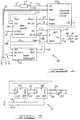
- FIG. 1 A functional block diagram of a programmable divider 100 arranged in accordance with the principles of the invention is set forth in FIG. 1. It is to be understood that the signal path interconnection shown between the functional blocks are two-wire differential interconnections which carry both the specified signal and its complement.
- a source of input pulses is coupled via path 115 to a prescaler 110 which, in the illustrative embodiment, is a divide-by-two circuit.
- the prescaler output at path 111 is coupled via path 111a to a CLK input of presettable count-down counter 120 and via path 111b to a CLK input of delay counter 130.
- Presettable count-down counter 120 has a multiple line parallel input data bus 170 presenting a digital representation of a numerical value to which the counter is to be preset. Bus 170 is directed to DATA inputs of counter 120.
- Counter 120 has an output designated EOC (end-of-count) coupled via path 112 to a START input of delay counter 130.
- Delay counter 130 has a divide-enable (DIV-EN) input coupled for receipt over path 116 of a divide-enable signal.
- Delay counter 130 has a PRESET control output 113 coupled via path 113 to a PRESET input of count-down counter 120 and an RC-EN control output coupled via path 114 to an ENABLE input of count-down counter 120.
- Delay counter 130 additionally includes a first output OUT coupled via path 117 to input A of multiplexer 140 and a second output HD-OUT coupled via path 118 and 118a to input B of multiplexer 140.
- Output HD-OUT of delay counter 130 is additionally coupled via path 118b to a CLK input of adder-accumulator 150.
- a divide-enable signal is additionally coupled via path 116a to a DIV-EN-L input of adder-accumulator 150.
- the least significant bit, PO, of information on bus 170 is coupled via path 171 to input IN of adder-accumulator 150.
- Adder-accumulator 150 has a CARRY output coupled via path 151, to a LONG-COUNT input of delay counter 130. Additionally, adder-accumulator 150 has a SUM output coupled via path 152 to the SELECT input of multiplexer 140.
- Multiplexer 140 has an output OUT coupled via path 119 to the input of output buffer 160 which in turn supplies a divider output 161 and its complement 162 for use by apparatus utilizing the divider of the invention.
- Prescaler 110 features circuitry which is symmetrical and fully differential, and it provides a differential output to drive the half integer divider comprised of elements 120, 130, 140, 150 and 160.
- the output 111 of prescaler 110 has the property that the output signal is the voltage difference between two symmetrical, active nodes, such that the complement of the signal is obtained with zero delay by reversing the connections to the output nodes, and the positive-going and negative-going output transitions are equally spaced in time.
- both the normal differential output signal and the complement differential output signal of the prescaler can be used as clock phases for the remainder of the circuitry of FIG. 1.
- the complement clock phase allows data transitions to be clocked at the time of the negative-going edge of the normal clock phase.
- Blocks 120, 130, 140, 150 and 160 form a true half-integer programmable divider capable of dividing by any integer or half-integer over a range determined by the width of data bus 170 and the delay incorporated into the delay counter 130 which will be discussed in more detail below.
- the divider of FIG. 1 When the divider of FIG. 1 is dividing by a half-integer, it provides equally spaced output pulses which are alternately clocked by a rising or falling edge of the prescaler output signal.
- P the presettable count-down counter 120
- P9 the delay counter 130
- EOC end-of-count
- the delay counter 130 is started by the EOC pulse on path 112 from counter 120 and, in the illustrative embodiment, on the fourth clock edge following the EOC pulse, delay counter 130 will enable counter 120 at its RC-EN output via path 114 to the ENABLE input of counter 120.
- counter 130 disables presettable counter 120, generates a preset pulse at output PRESET which is coupled via path 113 to the PRESET input of count-down counter 120 and generates the divider output pulse in undelayed and half-clock delayed forms, respectively, at output OUT and HD-OUT.
- delay counter 130 provides a one-half clock delayed version of the output pulse at output HD-OUT (clocked by the negative-going edge of the prescaler output, rather than the positive-going edge), and, when the LONG-COUNT input at path 151 is high, delay counter 130 enables count-down 120 after five clock pulses rather than four.
- adder-accumulator 150 control functions and the functions of multiplexer 140 are used for half-integer division. Division by N+1/2 can be approximated by alternatively dividing by N and N+1, but this produces unevenly spaced output pulses.
- evenly spaced output pulses at 161 and 162 are obtained by alternating between N and N+1 as the divisor and simultaneously using multiplexer 140 to select the divider output pulse alternately from the normal and the one-half clock delayed outputs of delay counter 130 at OUT, 117, and HD-OUT, 118, respectively.
- the divisor is N
- the output of the programmable divider is delayed one-half clock period
- the divisor is N+1
- the output is generated at the nominal time in phase with the signal transitions at prescaler output 111.
- This arrangement provides a string of output pulses evenly spaced every N+1/2 clock periods of the prescaler output.
- Adder-accumulator 150 adds the least significant bit PO to a running one-bit sum on each cycle of operation of the divider.
- the sum bit at output SUM controls multiplexer 140 over path 152 to select the normal or the half-bit-delayed outputs presented over paths 117 and 118a, respectively, to input A and B of multiplexer 140.
- the CARRY output of adder-accumulator 150 is used to enable the long (5 clock period) count of delay counter 130 by coupling an appropriate control signal via path 151 to the LONG-COUNT of delay counter 130.
- Output buffer 160 converts the low level differential logic signal coupled at path 119 to conventional ECL voltage levels for use by apparatus coupled to the divider output 161.
- the programmable divider has an overall modulus with a programmable increment less than the prescaler modulus and has a maximum operating frequency equal to a maximum operating frequency of the prescaler.
- prescaler 110 of FIG. 1 The logic diagram of prescaler 110 of FIG. 1 is set forth in FIG. 2.
- Input clock pulses are coupled via path 115 to a CLK input of D-type latch 210 and to a CLK input of D-latch 220, while an inverted or complimentary version of the input clock pulse train is coupled via path 215 to a CLK input of latch 210 and to a CLK input of latch 220.
- the Q output of latch 210 is coupled via path 211 to the D input of latch 220, while the Q output of latch 210 is coupled via path 212 to the D of latch 220.
- the Q output of latch 220 is coupled via path 221 to a first input of output buffer 230 and to the D input of latch 210, while the Q output of latch 220 is coupled via path 222 to a second input of differential output buffer 230 and to the D input of latch 210.
- prescaler 110 consists solely of D latches, and no logic gates are required between stages of the critical signal path. Since no intermediate logic gates are required between the latches, the arrangement shown is generally the fastest logic circuit which can be built with a given process technology. Additionally, with the arrangement shown, latch circuit modifications to increase speed can be effected without regard as to how such changes would affect the difficulty of coalescing logic gate functions into the latch itself.
- the half-integer divider portion of the overall arrangement of FIG. 1 is formed by the combination of presettable counter 120, delay counter 130, adder-accumulator 150 and the multiplexer 140.
- the details of the presettable count-down counter 120 are set forth in FIG. 4.
- Input CLK of count-down counter 120 over path 111a is coupled to a clock input of D latch 401a for which latch output Q follows input D when the clock input is low and latches when the clock input is high.
- Path 111a is additionally coupled to a clock input of D-latch 401b for which Q follows the D input when the clock is high and latches when the clock input is low.
- the ENABLE input at path 114 is coupled to a first input of AND gate 442 and to a first input of AND gate 441.
- the output of AND gate 442 is coupled to a first input of OR gate 443, while the output of AND gate 441 is coupled to a second input of OR gate 443.
- Programming data bit P1 is coupled via path 431 to a second input of AND gate 441.
- the output of OR gate 443 is coupled to the D input of latch 401a, while the Q output of latch 401a is coupled to the D input of latch 401b.
- the Q output of latch 401b is coupled via path 450-1 to a second input of AND gate 442 and to the clock inputs of latches 402a and 402b.
- the decoding logic chain for the count-down counter set forth in FIG. 4 is represented by a series of blocks 410-9 through 410-2, only two of which are specifically shown in the block diagram of FIG. 4.
- Each of the decoding chain blocks is designated A to represent the fact that the logic details set forth in block 410-9 are replicated in each of the blocks 410-2 through 410-8.
- the detailed functional interconnections will be set forth only with reference to the final or ninth stage of the counter depicted in FIG. 4.
- each stage of counter 120 is comprised of a pair of D-type latches with the clock inputs of each pair of a given stage coupled to the Q output of the second latch of a preceding stage and to the D input to the first latch of the pair of the preceding stage. Also, it will be understood that the Q output of the first latch of the pair of each stage is coupled to the D input of the second latch of the pair.
- the decoding logic at each stage of the decoding chain is replicated in each stage except the first.
- Each decoding logic stage may be described with reference to block 410-9.
- the highest order input data bit at P9 is coupled to a first input of OR gate 420 and to the P inputs of D-type latches 409a and 409b via path 439.
- the second input to OR gate 420 in the highest stage 410-9 of the decoding chain is coupled to static logic zero or low state V LO , and it will be understood that the corresponding second input to a replicated OR gate in the preceding stage will be coupled to path 411-9b.
- Output Q of latch 409b is coupled to a first input of OR gate 421 via path 450-9, while a second input at 412-9a is coupled to static logic zero or low state V LO at the highest order decoding logic block 410-9. It will be understood that a corresponding second input to a replicated gate 421 in a preceding stage will be coupled to path 412-9b.
- An output of OR gate 420 is coupled to path 411-9b and to a first input of AND gate 422.
- An output of OR gate 421 is coupled to a first input of AND gate 423.
- a PRESET input signal over path 113 is coupled to the PS inputs of all the D-type latches in stages 2 through 9 of counter 120 and additionally, is coupled via path 452-9 to a second input of AND gate 423 and a second input of AND gate 422.
- the outputs of AND gates 422 and 423 are respectively coupled to first and second inputs of OR gate 424 whose output 412-9b will be coupled to the second input of a replicated OR gate corresponding to gate 421 in a preceding decoding logic block A.
- the decoding chain has a final block corresponding to the first stage of the counter which is different from the decoding logic blocks 410-2 through 410-9, and this final decoding stage is comprised essentially or NOR gate 410-1.
- NOR gate 410-1 has a first input coupled via path 412-1 to output 412-2b of the second stage decoding block 410-2.
- a second input to NOR gate 410-1 is coupled to the Q output of first stage latch 401b.
- the logic elements arranged and as shown in FIG. 4 comprise a ripple counter. Only the first stage (latches 401a and 401b) is required to operate at the input clock rate carried via path 111a. Succeeding stages 2 through 9 operate at lower speeds and hence can be made to dissipate less power.
- the decoding logic shown allows all of the stages above the first to be identical except for changes in resistor values to scale the power.
- the preset function as controlled over path 113 presets each node of the decode chain rather than allowing the preset data to ripple through the stages of the ripple counter. This arrangement allows the preset to be accomplished in a much shorter time than would otherwise be feasible in other more conventional arrangements.
- the logic state to which each node in the counter is to be preset is provided by an ancillary decode chain controlled directly by the program data (P1-P9) as shown in the logic diagram 410-9, for example, of FIG. 4.
- the first counter stage comprised of latches 401a, and 401b is preset when the ENABLE input is logic high, or one, and is then free to count incoming pulses from the prescaler output via the CLK input when the ENABLE input is logic low or zero.
- the latches in the second and subsequent stages include a preset control input PS which overrides the clock input and sets the latches to the state present on the stage's corresponding data (P-) input.
- each node of the decoding chain is associated with a corresponding single counter stage.
- a decode chain utilizing three-input, rather than two-input, gates could have a node associated with two ripple counter stages.
- Other decoding arrangements with multiple nodes could also benefit from the concept of presetting to a value determined by a parallel decode chain.
- FIG. 4 To further improve the speed characteristics of the overall divider circuitry, it has been found preferable to coalesce logic elements such as shown schematically in FIG. 4 at gates 441, 442 and 443 into the D input of the latch element 401a itself.
- One example of a two-level series gate coalesced into the input of a differential D latch is set forth for example in FIG. 3. With the interconnections shown, the gate function illustrated in FIG. 3 is a two-input multiplexer. When CLK is a logic high or 1, the Q output of the circuit will equal (A*C) + (B*C) , which is the function performed by gates 441, 442, and 443 of FIG. 4. This coalescing approach is used wherever possible throughout the circuitry of FIG. 1 to improve the operating speed capability of the programmable divider disclosed.
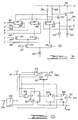
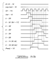
- the delay counter 130 of FIG. 1 is set forth in functional block diagram detail in FIG. 5A, and its operation is most easily explained by simultaneous reference to the timing diagram of FIG. 5B.
- START input at path 112 (which corresponds to the EOC output of count-down counter 120) is coupled to the D input of latch 501.
- the CLK input at path 111b is coupled to the clock inputs of D-type latches 501, 502, 503, 504, 505, 506, 507 and 508.
- the Q output of latch 501 is coupled via path 520 to a first input of OR gate 510.
- the Q output of latch 502 is coupled via path 521 to a first input of AND gate 512, to the OUT output at path 117 and to the D input of latch 506.
- the Q output of latch 503 is coupled via path 522 to a second input of OR gate 510 and to a first input of AND gate 514. Additionally, the Q output of latch 503 is coupled to the D input of latch 504.
- the Q output of latch 504 is coupled via path 523 to a D input of latch 505.
- the Q output of latch 505 is coupled to a first input of AND gate 515 and to a first input of NOR gate 513.
- the divide-enable input (DIV-EN) at path 116 is coupled to a second non-inverting input of NOR gate 513.
- the output of NOR gate 513 is coupled to a D input of latch 507, whose Q output is coupled via path 525 to a second inverting input of AND gate 512 and to a second input to NOR gate 511.
- An output of AND gate 512 comprises the PRESET output of the delay counter 130 at path 113.
- the HD-OUT output of the delay counter at path 118 is taken from the Q output of latch 506, while the RC-EN output of counter 130 at path 114 is taken from the Q output of latch 508.
- the LONG-COUNT input at path 151 is coupled to an inverting input of AND gate 514 and an input of AND gate 515.
- the outputs of AND gates 514 and 515 are respectively coupled to first and second inputs of OR gate 516, which has its output coupled to the D input of latch 508.
- the delay counter 130 of FIG. 1 consists of a master and slave latch arrangement with logic interspersed so as not to require more than a single two-level current steering gate between any two latches.
- the logic gates shown are all coalesced into the inputs of their corresponding latches.
- the START signal is identical to the end-of-count signal generated by the last gate in the decoder in the ripple counter of FIG. 4. That last decode gate of FIG. 4 designated 410-1 is coalesced into the input of latch 501.
- the ripple counter enable (RC-EN at path 114) goes to a logic low condition on the fourth clock edge after the START signal goes to a logic high state. If LONG-COUNT is logic high, latch 508 is driven from latch 505 rather than from latch 503, such that RC-EN goes to a logic low condition on the fifth edge after the START signal appears rather than after the fourth edge.
- the normal output signal for the divider to be fed to the multiplexer is taken from latch 502, and the one-half clock interval delayed output pulse is taken from latch 506.
- the delay counter varies between four and five delaying counts in accordance with the logic state of the signal appearing at the LONG-COUNT input at path 151.
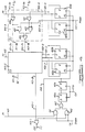
- FIG. 6 A functional block diagram of an adder-accumulator suitable for use with the invention is set forth in FIG. 6.
- the divide-enable input at path 116a is coupled to the input of a signal level shifter 610 having two outputs L1 and L3 which for logic state purposes, are identical.
- Output L1 of shifter 610 is coupled to a reset input of D latch 601 and to a reset input of D latch 604, while output L3 is coupled to a presetting input PS of latch 602.
- the least significant programming data bit PO is coupled via path 171 to a first input of coalesced AND gate 621 and to a first input of coalesced exclusive OR gate 622 and to the P input of latch 602.
- the HD OUT output of delay counter 130 is coupled via path 118b to the clock inputs of latches 601, 602, 603 and 604.
- the output of coalesced AND gate 621 is coupled to the B input of latch 601, while the output of coalesced exclusive OR gate 622 is coupled to the D input of latch 602.
- the CARRY output of the adder-accumulator at path 151 is taken from the Q output of latch 601, while the SUM output of the adder-accumulator at path 152 is taken from the Q output of latch 604.
- the Q output of latch 602 is coupled to the D input of latch 603.
- the Q output of latch 603 is coupled to the D input of latch 604 and to second inputs of both AND gates 621 and exclusive OR gate 622.
- the adder-accumulator has a CARRY output which goes high one divider cycle earlier than the SUM output.
- divisor data bit PO equals 1
- SUM logic 1
- CARRY logic zero on one cycle and with their respective logic states reversed on the next cycle. If the SUM output is then delayed one cycle, the CARRY and the delayed SUM outputs will cycle together alternating between both at logic one and both at logic zero. This is required for the programmable divider to correctly divide by a half-integer.
- the one bit adder-accumulator of FIG. 6 adds the input bit to the previous state of the accumulator and provides one SUM bit and one CARRY bit.
- the clock is phased such that the respective outputs change on the falling edge of the clock transitions.
- the SUM output selects between the normal and half-bit-delayed output pulses from delay counter 130 of FIG. 1, while the CARRY bit determines when the delay counter cycle is increased by one count.
- the multiplexer 140 and output buffer 160 of FIG. 1 are conventional differential circuits well known in the art. Therefore, their details are not further set forth in this description.
- the above description of the illustrative embodiment has assumed ideal operation in the sense that the delay from a clock edge at the prescaler input to the programmable divider output is independent of whether the nominal or the half-bit-delayed output of delay counter 130 is selected by multiplexer 140 in conjunction with adder-accumulator 150. In practice, this is not precisely correct, in that when the half-integer counter is operating in the half-integer mode there may be some small deviation from ideal timing on alternate output pulses of the overall programmable divider resulting in an unwanted subharmonic frequency component of the divider output. This would most easily be seen with a spectrum analyzer display of the divider output frequency.
- the observed subharmonic line is typically greater than 30 dB below the level that would be obtained if a simple alternation between divide-by-N and divide-by-N+1 were used to approximate the divide-by-(N+1/2) operation.
- the exact degree of suppression of the subharmonic depends on how accurately the clock-to-data delay is matched between the normal and the half-bit-delayed output. With careful circuit layout the clock-to-data delay can be matched well enough to avoid deleterious effects on the operation of a practical phase-locked-loop circuit.
- the half-integer divider disclosed with reference to FIG. 1 through FIG. 6 has a low minimum modulus, good speed/power performance and is easy to lay out as an LSI circuit, but the described approach is by no means the only practical construction for a half-integer divider operating in accordance with the principles of the invention.
- a pulse-swallowing counter based on a dual modulus prescaler and two control counters could probably be modified in accordance with the invention into a true half-integer divider, although it would be difficult to obtain a minimum modulus as low as that realized with the arrangement disclosed in FIG. 1.
- the circuit of FIG. 1 uses two output signals (the clock and its complement) from a prescaler to clock a half-integer divider to obtain overall integer programmability at the prescaler input.
- the divide-by-two prescaler can also be arranged to provide quadrature output so that all of the timing information available from both rising and falling edges of the input clock is preserved.
- One method of providing such quadrature outputs would be to use outputs from both latches 210 and 220 of prescaler 110 of FIG. 2. In this manner, all of the timing information available from both the rising and falling edges of the CLK input would be available for use by the programmable divider circuitry.
- a half-integer divider arranged in accordance with the invention could readily be extended to include a wider adder-accumulator multiplexer to select outputs with finer increments of delay, if all clock transitions from the prescaler were available to generate the delays.
- a quarter-integer divider could be used to give an overall half-integer programming capability at the prescaler input. In this case, the suppression of subharmonics in the divider output would be limited by the degree to which the positive and negative zero-crossings of the input clock were evenly spaced.
- the true fractional integer divider could even be clocked directly from an input signal with no prescaler, with the appropriate clock phases developed by hybrid junctions and summers. This would be potentially useful for minimizing the overall multiplication of the reference frequency in a phase-locked-loop synthesizer in which multiplied reference noise is a limitation. Such an approach would also allow for a faster settling time than could otherwise be achieved for a given output frequency spacing.
- FIG. 7 A second embodiment of a programmable divider designed in accordance with the principles of the invention is depicted in the block diagram of FIG. 7.
- the divider of FIG. 7 is substantially similar to that of FIG. 1, except for the output multiplexer 740 which is basically comprised of a clocked latch.
- a source of input pulses is coupled via path 715 to a prescaler 710 which, for this example, comprises a divide-by-two circuit.
- the prescaler output at path 711 is coupled via path 711a to a CLK input of count-down counter 720, via path 711b to a CLK input of delay counter 730, and via path 711c to a CLK input of output multiplexer 740.
- Presettable count-down counter 720 has a multiple line parallel input data bus 770 presenting a variable program-determined representation of a numerical value to which the counter is to be preset. Bus 770 is directed to DATA inputs of counter 720. Counter 720 has an output designated EOC (end-of-count) coupled via path 712 to a START input of delay counter 730.
- EOC end-of-count
- Delay counter 730 has a divide-enable (DIV-EN) input coupled for receipt over path 716 of a divide-enable signal.
- Delay counter 730 has a PRESET control output coupled via path 713 to a PRESET input of count-down counter 720 and a RC-EN control output coupled via path 714 to an ENABLE input of count-down counter 720.
- Delay counter 730 additionally includes a first output OUT coupled via path 717 to input A of multiplexer 740 and a second output HD-OUT coupled via path 718 to input B of multiplexer 740.
- Output 719 of multiplexer 740 is coupled via path 719a to a CLK input of adder-accumulator 750.
- a divide-enable signal is additionally coupled via path 716a to a DIV-EN-L input of adder-accumulator 750.
- the least significant bit, PO, of information on bus 770 is coupled via path 771 to input IN of adder-accumulator 750.
- Adder-accumulator 750 has a CARRY output coupled via path 751 to a LONG-COUNT input of delay counter 730. Additionally, adder-accumulator 750 has a SUM output coupled via path 752 to the SELECT input of multiplexer 740.
- Multiplexer 740 has an output OUT coupled via path 719 to the input of output buffer 760 which in turn supplies a divider output 761 and its complement 762 for use by apparatus utilizing the divider of the invention.
- Prescaler 710 like prescaler 110 of Fig. 1, features circuitry which is symmetrical and fully differential, and it provides a differential output to drive the half integer divider comprised of elements 720, 730, 740, 750 and 760.
- the output 711 of prescaler 710 has the property that the output signal is the voltage difference between two symmetrical, active nodes, such that the complement of the signal is obtained with zero delay by reversing the connections to the output nodes, and the positive-going and negative-going output transitions are equally spaced in time.
- both the positive-going edge and the negative-going edge of the prescaler output can be used as clock phases by the remainder of the circuitry of FIG. 7, as was the case for the embodiment of FIG. 1.
- the configuration and operation of the divider of FIG. 7 is substantially similar to that of FIG. 1, with two important exceptions.
- the first difference involves use of a clocked latch as the output multiplexer 740.
- the SUM output of adder-accumulator 750 causes multiplexer 740 to select, in one phase, a normal pulse from input A as the divider output, and, in a complementary phase, a half-bit delayed pulse from input B as the divider output.
- the advantage of the clocked multiplexer 740 is that there are fewer gates between the last clocked latch and the final divider output, in turn resulting in less final output timing jitter.
- the second difference is that the PRESET output of delay counter 730 is simply a buffered output of a latch analogous to latch 502 of FIG. 5A, rather than being the output of an AND gate such as 512 of FIG. 5A. This change provides a longer PRESET pulse to count-down counter 720, which eases the timing requirements in counter 720.
- Adder-accumulator 750 and multiplexer 740 of FIG. 7 are set forth in more functional detail in FIGS. 8 and 9, respectively.
- the remaining functional blocks of FIG. 7 are identical to their counterparts in FIG. 1, with the exception of the PRESET output of delay counter 730 discussed above.
- program bit PO at bus lead 771 is coupled to an inverting input of NOR gate 801 which has been coalesced into the D input of clocked latch 803. Additionally, lead 771 is coupled to a first input of exclusive OR gate 807 which has been coalesced into the D input of clocked latch 809.
- a clock signal for adder-accumulator 750 is taken from the output of multiplexer 740 at lead 719a and is coupled to clock inputs for latches 803, 805, and 809 of adder-accumulator 750.
- the CARRY output at path 751 is taken from a Q output of latch 803, while the SUM output at path 752 is taken from a Q output of latch 809.
- the Q output of latch 809 is additionally coupled to a D input of latch 805, whose Q output is coupled to a second input to exclusive OR gate 807 and to a non-inverting input of NOR gate 801.
- the A input to multiplexer 740 at path 717 is coupled to a non-inverting input of AND gate 901, while the B input at path 718 is coupled to a first input to AND gate 903.
- a select input at path 752 (which is coupled to the SUM output of the accumulator of FIG. 8) is coupled to a first input of exclusive NOR gate 909, a second input to AND gate 903 and an inverting input to AND gate 901.
- a clock input CLK at path 711c to multiplexer 740 is coupled to a second input to gate 909 which is coalesced into a clock input for D-type latch 907.
- gates 901 and 903 are respectively coupled to first and second inputs to OR gate 905 which is coalesced into the D input of latch 907.
- a Q output of latch 907 serves as a divider output at path 719 and as a source of clock pulses at path 719a for adder-accumulator 750 of FIGS. 7 and 8.
Landscapes
- Pulse Circuits (AREA)
- Stabilization Of Oscillater, Synchronisation, Frequency Synthesizers (AREA)
- Manipulation Of Pulses (AREA)
- Saccharide Compounds (AREA)
- Multi Processors (AREA)
- Memory System Of A Hierarchy Structure (AREA)
- Stored Programmes (AREA)
- Circuits Of Receivers In General (AREA)
Claims (13)
- Ein programmierbarer Teiler (100; 700) zum Teilen einer Pulswiederholungsrate eines Eingangspulszuges um eine vorausgewählte Zahl, wobei der programmierbare Teiler
eine programmierbare Zähleinrichtung (120, 130, 140, 150; 720,730,740,750) aufweist, welche einen Eingang (CLK) besitzt, der zum Empfang des Eingangspulszuges (111, 711) gekoppelt ist, und eine Dateneingangseinrichtung (170,171; 770, 771) zum Empfang von variablen Divisordaten (P₉-P₀), wobei die programmierbare Zähleinrichtung operativ ist, um einen Ausgangspulszug (119; 719) zu erzeugen, welcher im Durchschnitt eine Pulswiederholungsrate aufweist, die gleich einem Bruch der Eingangspuls-Zugpulswiederholungsrate durch Teilen der Eingangspuls-Zugpulswiederholungsrate um N oder um N+1 als Antwort auf ein Signal ist, welches von den Divisordaten abgeleitet ist, wobei N als eine Funktion der Divisordaten bestimmt ist; dadurch gekennzeichnet, daß
die programmierbare Zähleinrichtung eine Einrichtung (130,140,150; 730, 740, 750) zum genauen zeitlichen Trennen von Ausgangspulsen bei einem programmierbaren Teilerausgang für nicht ganzzahlige Werte des Divisors enthält;
die Einrichtung zum genauen Trennen der Ausgangspulse eine Einrichtung (130; 730) zum Vorsehen eines ersten Ausgangssignals (Out) und eines zweiten Ausgangssignals (HD-Out) aufweist, welches von dem ersten Ausgangssignal um eine halbe Periode der Pulse (111; 711) verzögert ist, und eine Einrichtung (140; 740), welche auf ein anderes Signal (152; 752) anspricht, welches von den Divisordaten (P₀) zum Auswählen entweder des ersten Ausgangssignals (Out), wenn eine Division um N +1 aufgetreten ist, oder des zweiten Ausgangssignals (HD-Out), wenn eine Division um N aufgetreten ist, abgeleitet ist, um das Ausgangssignal (119; 712) des Teilers zu bilden. - Ein programmierbarer Teiler nach Anspruch 1, dadurch gekennzeichnet, daß die Einrichtung zum genauen Trennen Vielfach-Taktphasen enthält, welche verwendet werden, um Zeitsteuerungssignale zu erzeugen, welche das genaue Trennen der Ausgangspulse gestatten.
- Ein programmierbarer Teiler nach Anspruch 2, desweiteren gekennzeichnet durch eine Vorteilereinrichtung (110; 710), welche einen Eingang (115; 715) aufweist, welcher zum Empfang des Eingangspulszuges gekoppelt ist und operativ ist, die Pulswiederholungsrate um einen vorherbestimmten Umrechnungsfaktor zu teilen, wobei die Vorteilereinrichtung wenigstens einen Ausgang (111; 711) zum Tragen von wenigstens zwei Phasen von den geteilten Vorteilerausgangspulsen aufweist, um die Vielfach-Taktphasen zu bilden.
- Ein programmierbarer Teiler nach einem der Ansprüche 1, 2 oder 3, dadurch gekennzeichnet, daß die programmierbare Zähleinrichtung der Division um N + 1/2 nahekommt durch wahlweises Teilen der Eingangspuls-Zugpulswiederholungsrate um N und N + 1, wobei N eine ganze Zahl ist, und wobei die Einrichtung zum genauen Trennen eine Einrichtung (130; 730) zum Verzögern eines Teilerausgangspulses um eine halbe Periode des Eingangspulszuges enthält, immer wenn der Divisor gleich N ist, und zum Hemmen der Verzögerung, immer wenn der Divisor N + 1 ist, wodurch ein Teilerausgangspulszug von Pulsen erzeugt wird, welche genau um N + 1/2 Perioden des Eingangspulszuges getrennt sind.
- Ein programmierbarer Teiler nach Anspruch 1, des weiteren gekennzeichnet durch
einen Vorteiler (110; 710), welcher einen Eingang (115; 715) besitzt, der zum Empfang des Eingangssignals gekoppelt ist und operativ ist, die Eingangssignalfrequenz durch einen Vorteiler-Umrechnungsfaktor zu teilen und das geteilte Frequenzsignal an einem Vorteilerausgang (111; 711) auszugeben, wobei die programmierbare Zähleinrichtung einen voreinstellbaren Count-down-Zähler (120; 720) aufweist, welcher einen Takteingang (CLK) besitzt, der an den Vorteilerausgang gekoppelt ist, eine Dateneingangseinrichtung (Data) zum Empfang der variablen Divisordaten und einen Ausgang (EOC), wobei der voreinstellbare Count-down-Zähler operativ ist, an seinem Ausgang (EOC) einen Zählende-Puls zu erzeugen, immer wenn eine Zahl von Pulsen, welche von dem Vorteilerausgang (111; 711) an dem Count-down-Zählertakteingang empfangen wurde, einer Zahl gleicht, die durch die variablen Divisordaten repräsentiert wird, und worin die Einrichtung zum genauen Trennen der Ausgangspulse einen Verzögerungszähler (130; 730) umfaßt, welcher an den Vorteilerausgang (111; 711) und an den voreinstellbaren Count-down-Zähler (120; 720) gekoppelt ist und die ersten (Out) und zweiten (HD-Out) Ausgänge besitzt, eine Verzögerungszähler-Steuereinrichtung (150; 750), welche an den Verzögerungszähler gekoppelt ist, und eine Wahleinrichtung (140; 740), welche an die ersten und zweiten Ausgänge des Verzögerungszählers und die Verzögerungszähler-Steuereinrichtung gekoppelt ist, und eine Ausgang (119; 719) besitzt, wobei der Verzögerungszähler, die Verzögerungszahler-Steuereinrichtung und die Wahleinrichtung als miteinander verbunden operativ sind, um den voreinstellbaren Count-down-Zähler (120; 720) für eine erste Zahl von Vorteiler-Ausgangspulsen von dem Empfang eines Ausgangspulses von dem Count-down-Zähler und für eine zweite Zahl von Vorteiler-Ausgangspulsen von dem Empfang des Ausgangspulses des Count-down-Zählers auf alternierende Count-down-Zähler-Operationszyklen zu deaktivieren, so daß die ersten (Out) und zweiten (HD-Out) Ausgangssignale des Verzögerungszählers (130; 730) zu dem Ausgang der Wahleinrichtung (119; 719) auf alternierende Zyklen der Operation des programmierbaren Teilers durchgelassen werden mit dem zweiten Verzögerungszählerausgangssignal (HD-Out), welches um eine halbe Periode der Vorteilerausgangspulsfrequenz im Hinblick auf das erste (Out) Verzögerungszählerausgangssignal verzögert wurde. - Ein programmierbarer Teiler nach Anspruch 5, dadurch gekennzeichnet, daß der Vorteiler (110) derart eingerichtet ist, daß sein Ausgang eine Spannungsdifferenz zwischen zwei symmetrischen aktiven Knoten (221,222) aufweist, so daß ein Komplement des Vorteiler-Ausgangssignals mit im wesentlichen keiner Verzögerung verfügbar ist, und wobei sowohl positiv als auch negativ verlaufende Flanken des Vorteiler-Ausgangssignals von dem Verzögerungszähler verwendet werden.
- Ein programmierbarer Teiler nach Anspruch 5 oder 6, dadurch gekennzeichnet, daß der voreinstellbare Count-down-Zähler einen Welligkeitszähler (401a-409a, 401b-409b) aufweist, und die Dateneingangseinrichtung eine Mehrzahl von parallelen Eingangsdatenleitungen (431-439) zum Tragen von Divisordaten aufweist, wobei eine Stufe des Welligkeitszählers an jede der Eingangsdatenleitungen gekoppelt ist.
- Ein programmierbarer Teiler nach Anspruch 7, dadurch gekennzeichnet, daß der Welligkeitszähler eine Dekodierlogik (410-1 bis 410-9) enthält, welche eine Mehrzahl von Knoten besitzt, wobei jeder Knoten mit wenigstens einer der Welligkeitszählerstufen und einer Einrichtung zum Voreinstellen sowohl der Welligkeitszählerstufen als auch der Knoten der Dekodierlogik in Übereinstimmung mit Daten zugeordnet ist, welche dem Welligkeitszähler über die Eingangsdatenleitungen ausgegeben werden.
- Ein programmierbarer Teiler nach einem der Ansprüche 5, 6, 7 oder 8, dadurch gekennzeichnet, daß die Verzögerungszähler-Steuereinrichtung einen Addierer-Akkumulator (150) aufweist, welcher einen Steuereingang (171) besitzt, der an eine der Eingangsdatenleitungen (P₀) gekoppelt ist, einen Takteingang (CLK), welcher an den zweiten Verzögerungszählerausgang (HD-Out) gekoppelt ist, einen Übertrag-Ausgang (151), welcher an einen Steuereingang (Long-Count) des Verzögerungszählers gekoppelt ist, und einen Summenausgang (152), welcher an die Wahleinrichtung gekoppelt ist, wobei der Addierer-Akkumulator operativ ist, ein Eingangssignal-Bit, welches einer der Eingangsdatenleitungen (P₀) ausgegeben wurde, einem vorhergehenden Zustand des Akkumulators hinzuzufügen, immer wenn der Takteingang (CLK) einem vorherbestimmten Übergang unterliegt, und um geeignete Summen- und Übertragslogikzustandsinformationen an den Summen- (152) bzw. Übertragsausgängen (151) bereitzustellen, wobei der Übertragsausgang (151) bestimmt, welcher der ersten und zweiten Zahlen von Vorteiler-Ausgangspulsen als Deaktivierungszeitperiode für den Count-down-Zähler verwendet werden soll, und wobei der Summenausgang (152) bestimmt, welcher der ersten und zweiten Ausgänge des Verzögerungszählers zu dem Ausgang der Wahleinrichtung durchgelassen werden soll.
- Ein programmierbarer Teiler nach Anspruch 9, dadurch gekennzeichnet, daß die Wahleinrichtung einen Multiplexer (140) aufweist, welcher erste (A) und zweite Eingänge (B) besitzt, die jeweils an die ersten (Out) und zweiten Ausgänge (HD-Out) des Verzögerungszählers (130) gekoppelt sind, und einen Wahl-Steuereingang (Select), welcher an den Summenausgang (152) des Addierer-Akkumulators (150) gekoppelt ist, wobei einer der ersten und zweiten Multiplexereingänge in Übereinstimmung mit einem binären Logikzustand des Wahl-Steuereingangs an einen Multiplexerausgang (119) gekoppelt ist.
- Ein programmierbarer Teiler nach Anspruch 10, des weiteren gekennzeichnet durch einen differentiellen Ausgangspuffer (160), welcher einen Eingang aufweist, der an den Multiplexerausgang (119) gekoppelt ist, und komplementäre Ausgänge (161,162), welche als Ausgänge des programmierbaren Teilers dienen.
- Ein programmierbarer Teiler nach einem der Ansprüche 5, 6 oder 7, dadurch gekennzeichnet, daß die Verzögerungszähler-Steuereinrichtung einen Addierer-Akkumulator (750) aufweist, welcher einen Steuereingang (771) aufweist, der an eine der Eingangsdatenleitungen (P₀) gekoppelt ist, einen Takteingang (CLK), welcher an den Ausgang der Wahleinrichtung (719) gekoppelt ist, einen Übertragsausgang (751), welcher an einen Steuereingang des Verzögerungszählers gekoppelt ist, und einen Summenausgang (752), welcher an die Wahleinrichtung (740) gekoppelt ist, wobei der Addierer-Akkumulator operativ ist, ein Eingangssignalbit, welches einer der Eingangsdatenleitungen (P₀) ausgegeben wurde, einem vorhergehenden Zustand des Akkumulators hinzuzufügen, immer wenn der Takteingang (CLK) einem vorherbestimmten Übergang unterliegt, und eine geeignete Summen- und Übertragslogikzustandsinformation den Summen- (752) bzw. Übertragsausgängen (751) bereitzustellen, wobei der Übertragsausgang (751) bestimmt, welcher der ersten und zweiten Zahlen von Vorteiler-Ausgangspulsen als eine Deaktivierungszeitperiode für den Count-down-Zähler verwendet werden soll, und der Summenausgang (752) bestimmt, welcher der ersten und zweiten Ausgänge des Verzögerungszählers zu dem Ausgang der Wahleinrichtung durchgelassen werden soll.
- Ein programmierbarer Teiler nach Anspruch 12, dadurch gekennzeichnet, daß die Wahleinrichtung einen Multiplexer (740) aufweist, welcher erste (A) und zweite Eingänge (B) besitzt, die jeweils an die ersten (Out) und zweiten Ausgänge (HD-Out) des Verzögerungszählers (730) gekoppelt sind, einen Wahl-Steuereingang (Select), welcher an den Summenausgang (752) des Addierer-Akkumulators (750) gekoppelt ist, und einen Takteingang (CLK), welcher an den Vorteilerausgang (711) gekoppelt ist, wobei der Multiplexer eine getaktete Latcheinrichtung (907) enthält, die auf einen vorherbestimmten Übergang eines Signals operabel ist, welches dem Takteingang (CLK) ausgegeben wurde, um einen der ersten (A) und zweiten Multiplexereingänge (B) an einen Ausgang der Latcheinrichtung (719) in Übereinstimmung mit einem Logikzustand des Wahl-Steuereingangs (Select) zu koppeln.
Applications Claiming Priority (3)
| Application Number | Priority Date | Filing Date | Title |
|---|---|---|---|
| US286435 | 1988-12-19 | ||
| US07/286,435 US4975931A (en) | 1988-12-19 | 1988-12-19 | High speed programmable divider |
| PCT/US1989/005003 WO1990007232A1 (en) | 1988-12-19 | 1989-11-14 | High speed programmable divider |
Publications (2)
| Publication Number | Publication Date |
|---|---|
| EP0406366A1 EP0406366A1 (de) | 1991-01-09 |
| EP0406366B1 true EP0406366B1 (de) | 1994-06-01 |
Family
ID=23098597
Family Applications (1)
| Application Number | Title | Priority Date | Filing Date |
|---|---|---|---|
| EP90900469A Expired - Lifetime EP0406366B1 (de) | 1988-12-19 | 1989-11-14 | Programmierbarer hochgeschwindigkeitsteiler |
Country Status (11)
| Country | Link |
|---|---|
| US (1) | US4975931A (de) |
| EP (1) | EP0406366B1 (de) |
| JP (1) | JP2577134B2 (de) |
| KR (1) | KR940007543B1 (de) |
| AU (1) | AU618434B2 (de) |
| CA (1) | CA2003466C (de) |
| DE (1) | DE68915756T2 (de) |
| ES (1) | ES2020823A6 (de) |
| IL (1) | IL92769A (de) |
| NO (1) | NO303308B1 (de) |
| WO (1) | WO1990007232A1 (de) |
Cited By (1)
| Publication number | Priority date | Publication date | Assignee | Title |
|---|---|---|---|---|
| DE19930179A1 (de) * | 1999-06-30 | 2001-01-25 | Infineon Technologies Ag | Hochgeschwindigkeitszähler |
Families Citing this family (35)
| Publication number | Priority date | Publication date | Assignee | Title |
|---|---|---|---|---|
| US5195111A (en) * | 1990-09-07 | 1993-03-16 | Nihon Musen Kabushiki Kaisha | Programmable frequency dividing apparatus |
| JP2842004B2 (ja) * | 1992-02-03 | 1998-12-24 | 日本電気株式会社 | 回路のテスト方式 |
| US5428769A (en) * | 1992-03-31 | 1995-06-27 | The Dow Chemical Company | Process control interface system having triply redundant remote field units |
| EP0602422A1 (de) * | 1992-12-15 | 1994-06-22 | International Business Machines Corporation | Dynamische Frequenzversetzung mit einem durch eins teilenden Taktgenerator |
| EP0683566A1 (de) * | 1994-05-17 | 1995-11-22 | Siemens Aktiengesellschaft | Schaltungsanordnung zum Teilen eines Taktsignals |
| DE19519321C2 (de) * | 1995-05-26 | 1997-10-16 | Gerhard Kultscher Ind Elektron | Frequenzteiler mit dualer, aktaler, dezimaler oder hexadezimaler Divisoreingabe |
| DE69631002T2 (de) * | 1995-09-28 | 2004-09-16 | Sanyo Electric Co., Ltd., Moriguchi | Einstellbarer Frequenzteiler |
| EP1020994A1 (de) * | 1995-11-22 | 2000-07-19 | Sanyo Electric Co., Ltd. | PLL mit variablem (N+1/2) Frequenzteiler-Verhältnis |
| FI100285B (fi) * | 1995-12-11 | 1997-10-31 | Nokia Mobile Phones Ltd | Taajuudenmuodostuspiiri |
| EP1005164B1 (de) * | 1996-01-09 | 2002-11-20 | SANYO ELECTRIC Co., Ltd. | Einstellbarer Frequenzteiler |
| US5748949A (en) * | 1996-07-02 | 1998-05-05 | Motorola Inc. | Counter having programmable periods and method therefor |
| US6065140A (en) * | 1997-04-30 | 2000-05-16 | Motorola, Inc. | Optimized computation of first and second divider values for a phase locked loop system |
| US5970110A (en) * | 1998-01-09 | 1999-10-19 | Neomagic Corp. | Precise, low-jitter fractional divider using counter of rotating clock phases |
| US6114915A (en) * | 1998-11-05 | 2000-09-05 | Altera Corporation | Programmable wide-range frequency synthesizer |
| US7003475B1 (en) | 1999-05-07 | 2006-02-21 | Medcohealth Solutions, Inc. | Computer implemented resource allocation model and process to dynamically and optimally schedule an arbitrary number of resources subject to an arbitrary number of constraints in the managed care, health care and/or pharmacy industry |
| KR100510844B1 (ko) * | 1999-08-21 | 2005-08-31 | 재단법인 포항산업과학연구원 | 중량 팔레트의 지지부재 최적위치 결정방법 |
| DE10002361C1 (de) | 2000-01-20 | 2001-01-25 | Infineon Technologies Ag | Frequenzteiler |
| US6789041B1 (en) * | 2001-05-08 | 2004-09-07 | Miranova Systems, Inc. | Bi-directional signal converter |
| US6690525B2 (en) * | 2001-05-25 | 2004-02-10 | Infineon Technologies Ag | High-speed programmable synchronous counter for use in a phase locked loop |
| US6975682B2 (en) * | 2001-06-12 | 2005-12-13 | Raytheon Company | Multi-bit delta-sigma analog-to-digital converter with error shaping |
| US6611573B2 (en) * | 2001-08-14 | 2003-08-26 | Sun Microsystems, Inc. | Non-integer division of frequency |
| RU2222101C2 (ru) * | 2002-01-08 | 2004-01-20 | Федеральное государственное унитарное предприятие Омский научно-исследовательский институт приборостроения | Делитель частоты с дробным переменным коэффициентом деления |
| US6725245B2 (en) | 2002-05-03 | 2004-04-20 | P.C. Peripherals, Inc | High speed programmable counter architecture |
| US6879654B2 (en) * | 2003-04-25 | 2005-04-12 | International Business Machines Corporation | Non-integer frequency divider circuit |
| US7336756B2 (en) * | 2004-10-25 | 2008-02-26 | Miranova Systems, Inc. | Reprogrammable bi-directional signal converter |
| US7231012B2 (en) * | 2004-11-30 | 2007-06-12 | Stmicroelectronics Pvt. Ltd. | Programmable frequency divider |
| US8149022B2 (en) * | 2007-02-09 | 2012-04-03 | Mediatek Inc. | Digital delay line based frequency synthesizer |
| US8131242B2 (en) * | 2007-07-02 | 2012-03-06 | Sony Corporation | System and method for implementing a swap function for an IQ generator |
| US7724097B2 (en) * | 2008-08-28 | 2010-05-25 | Resonance Semiconductor Corporation | Direct digital synthesizer for reference frequency generation |
| US8242850B2 (en) * | 2008-08-28 | 2012-08-14 | Resonance Semiconductor Corporation | Direct digital synthesizer for reference frequency generation |
| EP2806562A1 (de) * | 2013-05-22 | 2014-11-26 | Asahi Kasei Microdevices Corporation | Programmierbares Frequenzteilermodul mit Arbeitszyklus bei fast fünfzig Prozent |
| US9106216B1 (en) * | 2014-07-31 | 2015-08-11 | Microsoft Technology Licensing Llc | Programmable pulse generation |
| US10812090B2 (en) * | 2018-11-26 | 2020-10-20 | Stmicroelectronics S.R.L. | Ultra-low power, real time clock generator and jitter compensation method |
| CN113381752B (zh) * | 2021-06-24 | 2023-02-28 | 成都纳能微电子有限公司 | 半分频电路及方法 |
| US11874693B2 (en) | 2022-05-24 | 2024-01-16 | Analog Devices International Unlimited Company | Reconfigurable clock divider |
Family Cites Families (23)
| Publication number | Priority date | Publication date | Assignee | Title |
|---|---|---|---|---|
| US3873815A (en) * | 1973-03-19 | 1975-03-25 | Farinon Electric | Frequency division by an odd integer factor |
| US3959737A (en) * | 1974-11-18 | 1976-05-25 | Engelmann Microwave Co. | Frequency synthesizer having fractional frequency divider in phase-locked loop |
| US4017719A (en) * | 1975-12-18 | 1977-04-12 | Rca Corporation | Binary rate multiplier with means for spacing output signals |
| US4193037A (en) * | 1978-03-20 | 1980-03-11 | Motorola, Inc. | Frequency divider circuit with selectable integer/non-integer division |
| DE2826321C3 (de) * | 1978-06-15 | 1981-02-26 | Siemens Ag, 1000 Berlin Und 8000 Muenchen | Digitaler Frequenzteiler |
| JPS5637734A (en) * | 1979-09-04 | 1981-04-11 | Matsushita Electric Ind Co Ltd | Frequency dividing device |
| JPS5718129A (en) * | 1980-07-07 | 1982-01-29 | Nec Corp | Pulse swallow frequency divider |
| JPS5718128A (en) * | 1980-07-08 | 1982-01-29 | Yamatake Honeywell Co Ltd | Frequency dividing circuit |
| JPS5733471A (en) * | 1980-07-31 | 1982-02-23 | Fujitsu Ltd | Memory access control system for multiprocessor |
| JPS57133728A (en) * | 1981-02-12 | 1982-08-18 | Matsushita Electric Ind Co Ltd | Frequency divider |
| JPS59135684A (ja) * | 1983-01-24 | 1984-08-03 | Fujitsu Ltd | バツフアメモリ間のデ−タバイパス方式 |
| JPS59190724A (ja) * | 1983-04-14 | 1984-10-29 | Fuji Electric Co Ltd | 周波数可変のパルス発生器 |
| JPS603228A (ja) * | 1983-06-20 | 1985-01-09 | Nec Home Electronics Ltd | 分周回路 |
| US4555793A (en) * | 1983-11-28 | 1985-11-26 | Allied Corporation | Averaging non-integer frequency division apparatus |
| US4773031A (en) * | 1984-12-24 | 1988-09-20 | Tektronix, Inc. | Method and circuit for digital frequency multiplication |
| US4623846A (en) | 1985-02-14 | 1986-11-18 | Motorola, Inc. | Constant duty cycle, frequency programmable clock generator |
| US4658406A (en) * | 1985-08-12 | 1987-04-14 | Andreas Pappas | Digital frequency divider or synthesizer and applications thereof |
| JPS62120553A (ja) * | 1985-11-20 | 1987-06-01 | Nec Corp | 命令キヤツシユメモリ方式 |
| US4837721A (en) * | 1986-06-30 | 1989-06-06 | Itt Defense Communications, A Division Of Itt Corporation | Digital divider with integer and fractional division capability |
| US4856032A (en) * | 1987-01-12 | 1989-08-08 | Motorola, Inc. | High speed programmable frequency divider and PLL |
| US4809221A (en) * | 1987-01-28 | 1989-02-28 | Megatest Corporation | Timing signal generator |
| DE3705629A1 (de) * | 1987-02-21 | 1988-09-01 | Thomson Brandt Gmbh | Programmierbarer frequenzteiler sowie verfahren zur erzeugung eines niederfrequenten signals aus einem hochfrequenten signal |
| US4807266A (en) * | 1987-09-28 | 1989-02-21 | Compaq Computer Corporation | Circuit and method for performing equal duty cycle odd value clock division and clock synchronization |
-
1988
- 1988-12-19 US US07/286,435 patent/US4975931A/en not_active Expired - Lifetime
-
1989
- 1989-11-14 DE DE68915756T patent/DE68915756T2/de not_active Expired - Fee Related
- 1989-11-14 EP EP90900469A patent/EP0406366B1/de not_active Expired - Lifetime
- 1989-11-14 KR KR1019900701784A patent/KR940007543B1/ko not_active Expired - Fee Related
- 1989-11-14 WO PCT/US1989/005003 patent/WO1990007232A1/en not_active Ceased
- 1989-11-14 JP JP2500380A patent/JP2577134B2/ja not_active Expired - Lifetime
- 1989-11-14 AU AU46538/89A patent/AU618434B2/en not_active Ceased
- 1989-11-21 CA CA002003466A patent/CA2003466C/en not_active Expired - Fee Related
- 1989-12-18 ES ES8904257A patent/ES2020823A6/es not_active Expired - Lifetime
- 1989-12-18 IL IL92769A patent/IL92769A/xx not_active IP Right Cessation
-
1990
- 1990-08-16 NO NO903620A patent/NO303308B1/no unknown
Cited By (2)
| Publication number | Priority date | Publication date | Assignee | Title |
|---|---|---|---|---|
| DE19930179A1 (de) * | 1999-06-30 | 2001-01-25 | Infineon Technologies Ag | Hochgeschwindigkeitszähler |
| DE19930179C2 (de) * | 1999-06-30 | 2001-07-05 | Infineon Technologies Ag | Hochgeschwindigkeitszähler |
Also Published As
| Publication number | Publication date |
|---|---|
| NO903620L (no) | 1990-08-16 |
| CA2003466C (en) | 1995-01-31 |
| IL92769A (en) | 1993-02-21 |
| DE68915756D1 (de) | 1994-07-07 |
| US4975931A (en) | 1990-12-04 |
| JP2577134B2 (ja) | 1997-01-29 |
| DE68915756T2 (de) | 1994-09-22 |
| AU4653889A (en) | 1990-07-10 |
| WO1990007232A1 (en) | 1990-06-28 |
| ES2020823A6 (es) | 1991-10-01 |
| IL92769A0 (en) | 1990-09-17 |
| KR940007543B1 (ko) | 1994-08-19 |
| CA2003466A1 (en) | 1990-06-19 |
| KR910700567A (ko) | 1991-03-15 |
| NO303308B1 (no) | 1998-06-22 |
| EP0406366A1 (de) | 1991-01-09 |
| JPH03502870A (ja) | 1991-06-27 |
| AU618434B2 (en) | 1991-12-19 |
| NO903620D0 (no) | 1990-08-16 |
Similar Documents
| Publication | Publication Date | Title |
|---|---|---|
| EP0406366B1 (de) | Programmierbarer hochgeschwindigkeitsteiler | |
| US5537068A (en) | Differential delay line clock generator | |
| US6914460B1 (en) | Counter-based clock doubler circuits and methods | |
| CN110830041B (zh) | 占空比50%的连续整数分频器及包括其的锁相环电路 | |
| US5828250A (en) | Differential delay line clock generator with feedback phase control | |
| US5065415A (en) | Programmable frequency divider | |
| US6542013B1 (en) | Fractional divisors for multiple-phase PLL systems | |
| US6661261B2 (en) | Programmable divider with built-in programmable delay chain for high-speed/low power application | |
| JPS6243568B2 (de) | ||
| CA1137568A (en) | Digital phase comparator circuit | |
| US6489817B1 (en) | Clock divider using positive and negative edge triggered state machines | |
| EP0954106B1 (de) | Taktsignal-Vervielfacherschaltung für eine Tatksignalgeneratorschaltung | |
| CN1044556A (zh) | 高速预分频器 | |
| US6906571B1 (en) | Counter-based phased clock generator circuits and methods | |
| US20020186808A1 (en) | Fully programmable multimodulus prescaler | |
| US7034584B2 (en) | Apparatus for frequency dividing a master clock signal by a non-integer | |
| US5384816A (en) | Frequency divider circuit | |
| US6316982B1 (en) | Digital clock with controllable phase skew | |
| US6404839B1 (en) | Selectable clock divider circuit with a 50% duty cycle clock | |
| KR100795173B1 (ko) | 주파수 합성기 | |
| US6108393A (en) | Enhanced prescaler phase interface | |
| US20090122950A1 (en) | AFSM circuit and method for low jitter PLL CMOS programmable divider | |
| CN120320767B (zh) | 一种输出占空比50%的连续整数分频器 | |
| KR200164990Y1 (ko) | 50% 듀티의 홀수분주기 | |
| US4081755A (en) | Baud rate generator utilizing single clock source |
Legal Events
| Date | Code | Title | Description |
|---|---|---|---|
| PUAI | Public reference made under article 153(3) epc to a published international application that has entered the european phase |
Free format text: ORIGINAL CODE: 0009012 |
|
| AK | Designated contracting states |
Kind code of ref document: A1 Designated state(s): CH DE FR GB IT LI NL SE |
|
| 17P | Request for examination filed |
Effective date: 19901204 |
|
| 17Q | First examination report despatched |
Effective date: 19930128 |
|
| GRAA | (expected) grant |
Free format text: ORIGINAL CODE: 0009210 |
|
| AK | Designated contracting states |
Kind code of ref document: B1 Designated state(s): CH DE FR GB IT LI NL SE |
|
| REF | Corresponds to: |
Ref document number: 68915756 Country of ref document: DE Date of ref document: 19940707 |
|
| ET | Fr: translation filed | ||
| ITF | It: translation for a ep patent filed | ||
| EAL | Se: european patent in force in sweden |
Ref document number: 90900469.9 |
|
| PLBE | No opposition filed within time limit |
Free format text: ORIGINAL CODE: 0009261 |
|
| STAA | Information on the status of an ep patent application or granted ep patent |
Free format text: STATUS: NO OPPOSITION FILED WITHIN TIME LIMIT |
|
| 26N | No opposition filed | ||
| PGFP | Annual fee paid to national office [announced via postgrant information from national office to epo] |
Ref country code: CH Payment date: 19961030 Year of fee payment: 8 |
|
| PG25 | Lapsed in a contracting state [announced via postgrant information from national office to epo] |
Ref country code: LI Free format text: LAPSE BECAUSE OF NON-PAYMENT OF DUE FEES Effective date: 19971130 Ref country code: CH Free format text: LAPSE BECAUSE OF NON-PAYMENT OF DUE FEES Effective date: 19971130 |
|
| REG | Reference to a national code |
Ref country code: CH Ref legal event code: PL |
|
| REG | Reference to a national code |
Ref country code: GB Ref legal event code: 732E |
|
| NLS | Nl: assignments of ep-patents |
Owner name: RAYTHEON COMPANY;HE HOLDINGS, INC. |
|
| REG | Reference to a national code |
Ref country code: FR Ref legal event code: TP Ref country code: FR Ref legal event code: CD Ref country code: FR Ref legal event code: CA |
|
| REG | Reference to a national code |
Ref country code: GB Ref legal event code: IF02 |
|
| PGFP | Annual fee paid to national office [announced via postgrant information from national office to epo] |
Ref country code: FR Payment date: 20031125 Year of fee payment: 15 |
|
| PGFP | Annual fee paid to national office [announced via postgrant information from national office to epo] |
Ref country code: DE Payment date: 20031128 Year of fee payment: 15 |
|
| PGFP | Annual fee paid to national office [announced via postgrant information from national office to epo] |
Ref country code: NL Payment date: 20031130 Year of fee payment: 15 |
|
| PGFP | Annual fee paid to national office [announced via postgrant information from national office to epo] |
Ref country code: GB Payment date: 20040112 Year of fee payment: 15 |
|
| PGFP | Annual fee paid to national office [announced via postgrant information from national office to epo] |
Ref country code: SE Payment date: 20040401 Year of fee payment: 15 |
|
| PG25 | Lapsed in a contracting state [announced via postgrant information from national office to epo] |
Ref country code: GB Free format text: LAPSE BECAUSE OF NON-PAYMENT OF DUE FEES Effective date: 20041114 |
|
| PG25 | Lapsed in a contracting state [announced via postgrant information from national office to epo] |
Ref country code: SE Free format text: LAPSE BECAUSE OF NON-PAYMENT OF DUE FEES Effective date: 20041115 |
|
| PG25 | Lapsed in a contracting state [announced via postgrant information from national office to epo] |
Ref country code: NL Free format text: LAPSE BECAUSE OF NON-PAYMENT OF DUE FEES Effective date: 20050601 Ref country code: DE Free format text: LAPSE BECAUSE OF NON-PAYMENT OF DUE FEES Effective date: 20050601 |
|
| EUG | Se: european patent has lapsed | ||
| GBPC | Gb: european patent ceased through non-payment of renewal fee |
Effective date: 20041114 |
|
| PG25 | Lapsed in a contracting state [announced via postgrant information from national office to epo] |
Ref country code: FR Free format text: LAPSE BECAUSE OF NON-PAYMENT OF DUE FEES Effective date: 20050729 |
|
| NLV4 | Nl: lapsed or anulled due to non-payment of the annual fee |
Effective date: 20050601 |
|
| REG | Reference to a national code |
Ref country code: FR Ref legal event code: ST |
|
| PG25 | Lapsed in a contracting state [announced via postgrant information from national office to epo] |
Ref country code: IT Free format text: LAPSE BECAUSE OF NON-PAYMENT OF DUE FEES Effective date: 20051114 |
|
| REG | Reference to a national code |
Ref country code: GB Ref legal event code: 732E Free format text: REGISTERED BETWEEN 20090910 AND 20090916 |
|
| REG | Reference to a national code |
Ref country code: GB Ref legal event code: 732E Free format text: REGISTERED BETWEEN 20090917 AND 20090923 |