EP0408272A2 - Liaison de conducteurs électriques - Google Patents
Liaison de conducteurs électriques Download PDFInfo
- Publication number
- EP0408272A2 EP0408272A2 EP90307447A EP90307447A EP0408272A2 EP 0408272 A2 EP0408272 A2 EP 0408272A2 EP 90307447 A EP90307447 A EP 90307447A EP 90307447 A EP90307447 A EP 90307447A EP 0408272 A2 EP0408272 A2 EP 0408272A2
- Authority
- EP
- European Patent Office
- Prior art keywords
- conductor
- bonding
- support member
- wire
- integrated circuit
- Prior art date
- Legal status (The legal status is an assumption and is not a legal conclusion. Google has not performed a legal analysis and makes no representation as to the accuracy of the status listed.)
- Withdrawn
Links
Images

Classifications
-
- H—ELECTRICITY
- H10—SEMICONDUCTOR DEVICES; ELECTRIC SOLID-STATE DEVICES NOT OTHERWISE PROVIDED FOR
- H10W—GENERIC PACKAGES, INTERCONNECTIONS, CONNECTORS OR OTHER CONSTRUCTIONAL DETAILS OF DEVICES COVERED BY CLASS H10
- H10W72/00—Interconnections or connectors in packages
- H10W72/071—Connecting or disconnecting
- H10W72/075—Connecting or disconnecting of bond wires
-
- H—ELECTRICITY
- H10—SEMICONDUCTOR DEVICES; ELECTRIC SOLID-STATE DEVICES NOT OTHERWISE PROVIDED FOR
- H10W—GENERIC PACKAGES, INTERCONNECTIONS, CONNECTORS OR OTHER CONSTRUCTIONAL DETAILS OF DEVICES COVERED BY CLASS H10
- H10W72/00—Interconnections or connectors in packages
- H10W72/071—Connecting or disconnecting
- H10W72/0711—Apparatus therefor
-
- H—ELECTRICITY
- H10—SEMICONDUCTOR DEVICES; ELECTRIC SOLID-STATE DEVICES NOT OTHERWISE PROVIDED FOR
- H10W—GENERIC PACKAGES, INTERCONNECTIONS, CONNECTORS OR OTHER CONSTRUCTIONAL DETAILS OF DEVICES COVERED BY CLASS H10
- H10W72/00—Interconnections or connectors in packages
- H10W72/50—Bond wires
-
- H—ELECTRICITY
- H10—SEMICONDUCTOR DEVICES; ELECTRIC SOLID-STATE DEVICES NOT OTHERWISE PROVIDED FOR
- H10W—GENERIC PACKAGES, INTERCONNECTIONS, CONNECTORS OR OTHER CONSTRUCTIONAL DETAILS OF DEVICES COVERED BY CLASS H10
- H10W72/00—Interconnections or connectors in packages
- H10W72/071—Connecting or disconnecting
- H10W72/0711—Apparatus therefor
- H10W72/07141—Means for applying energy, e.g. ovens or lasers
-
- H—ELECTRICITY
- H10—SEMICONDUCTOR DEVICES; ELECTRIC SOLID-STATE DEVICES NOT OTHERWISE PROVIDED FOR
- H10W—GENERIC PACKAGES, INTERCONNECTIONS, CONNECTORS OR OTHER CONSTRUCTIONAL DETAILS OF DEVICES COVERED BY CLASS H10
- H10W72/00—Interconnections or connectors in packages
- H10W72/071—Connecting or disconnecting
- H10W72/075—Connecting or disconnecting of bond wires
- H10W72/07502—Connecting or disconnecting of bond wires using an auxiliary member
-
- H—ELECTRICITY
- H10—SEMICONDUCTOR DEVICES; ELECTRIC SOLID-STATE DEVICES NOT OTHERWISE PROVIDED FOR
- H10W—GENERIC PACKAGES, INTERCONNECTIONS, CONNECTORS OR OTHER CONSTRUCTIONAL DETAILS OF DEVICES COVERED BY CLASS H10
- H10W72/00—Interconnections or connectors in packages
- H10W72/071—Connecting or disconnecting
- H10W72/075—Connecting or disconnecting of bond wires
- H10W72/07521—Aligning
-
- H—ELECTRICITY
- H10—SEMICONDUCTOR DEVICES; ELECTRIC SOLID-STATE DEVICES NOT OTHERWISE PROVIDED FOR
- H10W—GENERIC PACKAGES, INTERCONNECTIONS, CONNECTORS OR OTHER CONSTRUCTIONAL DETAILS OF DEVICES COVERED BY CLASS H10
- H10W72/00—Interconnections or connectors in packages
- H10W72/071—Connecting or disconnecting
- H10W72/075—Connecting or disconnecting of bond wires
- H10W72/07531—Techniques
- H10W72/07532—Compression bonding, e.g. thermocompression bonding
- H10W72/07533—Ultrasonic bonding, e.g. thermosonic bonding
-
- H—ELECTRICITY
- H10—SEMICONDUCTOR DEVICES; ELECTRIC SOLID-STATE DEVICES NOT OTHERWISE PROVIDED FOR
- H10W—GENERIC PACKAGES, INTERCONNECTIONS, CONNECTORS OR OTHER CONSTRUCTIONAL DETAILS OF DEVICES COVERED BY CLASS H10
- H10W72/00—Interconnections or connectors in packages
- H10W72/50—Bond wires
- H10W72/531—Shapes of wire connectors
- H10W72/533—Cross-sectional shape
- H10W72/534—Cross-sectional shape being rectangular
-
- H—ELECTRICITY
- H10—SEMICONDUCTOR DEVICES; ELECTRIC SOLID-STATE DEVICES NOT OTHERWISE PROVIDED FOR
- H10W—GENERIC PACKAGES, INTERCONNECTIONS, CONNECTORS OR OTHER CONSTRUCTIONAL DETAILS OF DEVICES COVERED BY CLASS H10
- H10W72/00—Interconnections or connectors in packages
- H10W72/50—Bond wires
- H10W72/531—Shapes of wire connectors
- H10W72/5363—Shapes of wire connectors the connected ends being wedge-shaped
-
- H—ELECTRICITY
- H10—SEMICONDUCTOR DEVICES; ELECTRIC SOLID-STATE DEVICES NOT OTHERWISE PROVIDED FOR
- H10W—GENERIC PACKAGES, INTERCONNECTIONS, CONNECTORS OR OTHER CONSTRUCTIONAL DETAILS OF DEVICES COVERED BY CLASS H10
- H10W72/00—Interconnections or connectors in packages
- H10W72/50—Bond wires
- H10W72/551—Materials of bond wires
- H10W72/552—Materials of bond wires comprising metals or metalloids, e.g. silver
- H10W72/5522—Materials of bond wires comprising metals or metalloids, e.g. silver comprising gold [Au]
-
- H—ELECTRICITY
- H10—SEMICONDUCTOR DEVICES; ELECTRIC SOLID-STATE DEVICES NOT OTHERWISE PROVIDED FOR
- H10W—GENERIC PACKAGES, INTERCONNECTIONS, CONNECTORS OR OTHER CONSTRUCTIONAL DETAILS OF DEVICES COVERED BY CLASS H10
- H10W72/00—Interconnections or connectors in packages
- H10W72/50—Bond wires
- H10W72/551—Materials of bond wires
- H10W72/552—Materials of bond wires comprising metals or metalloids, e.g. silver
- H10W72/5524—Materials of bond wires comprising metals or metalloids, e.g. silver comprising aluminium [Al]
-
- H—ELECTRICITY
- H10—SEMICONDUCTOR DEVICES; ELECTRIC SOLID-STATE DEVICES NOT OTHERWISE PROVIDED FOR
- H10W—GENERIC PACKAGES, INTERCONNECTIONS, CONNECTORS OR OTHER CONSTRUCTIONAL DETAILS OF DEVICES COVERED BY CLASS H10
- H10W72/00—Interconnections or connectors in packages
- H10W72/50—Bond wires
- H10W72/551—Materials of bond wires
- H10W72/552—Materials of bond wires comprising metals or metalloids, e.g. silver
- H10W72/5525—Materials of bond wires comprising metals or metalloids, e.g. silver comprising copper [Cu]
-
- H—ELECTRICITY
- H10—SEMICONDUCTOR DEVICES; ELECTRIC SOLID-STATE DEVICES NOT OTHERWISE PROVIDED FOR
- H10W—GENERIC PACKAGES, INTERCONNECTIONS, CONNECTORS OR OTHER CONSTRUCTIONAL DETAILS OF DEVICES COVERED BY CLASS H10
- H10W72/00—Interconnections or connectors in packages
- H10W72/50—Bond wires
- H10W72/59—Bond pads specially adapted therefor
-
- H—ELECTRICITY
- H10—SEMICONDUCTOR DEVICES; ELECTRIC SOLID-STATE DEVICES NOT OTHERWISE PROVIDED FOR
- H10W—GENERIC PACKAGES, INTERCONNECTIONS, CONNECTORS OR OTHER CONSTRUCTIONAL DETAILS OF DEVICES COVERED BY CLASS H10
- H10W72/00—Interconnections or connectors in packages
- H10W72/90—Bond pads, in general
- H10W72/951—Materials of bond pads
- H10W72/952—Materials of bond pads comprising metals or metalloids, e.g. PbSn, Ag or Cu
-
- H—ELECTRICITY
- H10—SEMICONDUCTOR DEVICES; ELECTRIC SOLID-STATE DEVICES NOT OTHERWISE PROVIDED FOR
- H10W—GENERIC PACKAGES, INTERCONNECTIONS, CONNECTORS OR OTHER CONSTRUCTIONAL DETAILS OF DEVICES COVERED BY CLASS H10
- H10W90/00—Package configurations
- H10W90/701—Package configurations characterised by the relative positions of pads or connectors relative to package parts
- H10W90/751—Package configurations characterised by the relative positions of pads or connectors relative to package parts of bond wires
- H10W90/754—Package configurations characterised by the relative positions of pads or connectors relative to package parts of bond wires between a chip and a stacked insulating package substrate, interposer or RDL
Definitions
- the invention relates to the bonding of electrical conductors to integrated circuit devices, for example in the manufacture of semiconductor devices and in particular to a new method for attaching leads to an integrated circuit chip.
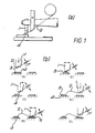
- Ultrasonic bonding of fine wires is well-known, such as wedge bonding in which an ultrasonic head containing a welding tool 1 (Figure 1) feeding the wire 2 makes a first joint on a suitable prepared metallised pad 3 on a silicon chip 4. ( Figure 1 b(1) and b(2)). The tool head 1 is moved relative to the chip ( Figure 1b(3) and b(4)) to pull out a length of wire 2 and make a second joint to a suitable prepared metallised pad 5 or an external circuit track (Figure 1b(5)). This latter joint is sufficiently strong and the wire 2 sufficiently deformed for the wire to be broken off at this point ( Figure 1 b(6)) in preparation for a subsequent wire connection from the silicon chip.
- the wire passes coaxially through the welding tool 7 ( Figure 2) and subsequently a ball 8 is formed on the end of the wire 9 by melting.
- the ball diameter is twice the wire diameter.
- This is then pressed into contact with the metallisation 10 on the silicon chip 11 to produce a bond at a suitable elevated temperature or by the application of ultrasonic energy.
- This particular arrangement has the advantage that the wire can be led off in any direction (since the ball bond is symmetrical about the axis of the wire) with a subsequent capillary wedge bond external to the chip on to the appropriate circuit track.
- the disadvantage of ball bonding is that the ball is deformed and typically extends over some four wire diameters.
- tape automatic bonding Another method of manufacture which has been known for about 20 years is so-called tape automatic bonding (TAB).
- TAB tape automatic bonding
- the electrical connections are etched in a foil which in turn is bonded to the metallised pads on the silicon chip.
- the tape comprises either a plain etched metal foil, or alternatively an etched metallised layer attached to a plastic film which acts as a carrier, or thirdly the etched metallised layer in conjunction with an adhesive which is carried on the plastic tape.
- a method of bonding an electrical conductor to a contact of an integrated circuit device comprises bonding a conductor to a support member and to a contact of an integrated circuit device; and subsequently severing the bonded conductor to release the integrated circuit device and the bonded conductor from the conductor support member.
- the device is temporarily connected to the support member to allow testing to be performed.
- the support member is then separated from the device leaving a free end of the conductor which can be permanently bonded to a final carrier.
- the integrated circuit device will comprise a silicon chip although other devices could also be used.
- the conductor may be in the form of a wire or ribbon.
- a second method permanent connections are made to a silicon chip by standard wire (or preferably rectangular ribbon) using a wedge bonding machine with the wire or ribbon subsequently being bonded to a support member constituting an intermediary substrate for handling purposes.
- a first bond is made on the silicon chip and the second temporary bond or attachment is accomplished between the connecting lead and the temporary substrate or support member (carrier).
- the bonds to the temporary support do not have to be of high integrity in the long term but only sufficiently strong to enable the wire or ribbon to be readily broken following this second (temporary) attachment to the carrier substrate.
- the (temporary) bonds on the intermediary substrate or support member can if necessary be reinforced by bonding a cap or lid to entrap the wires or preferably ribbons on to the intermediary substrate. Again, since only a limited mechanical strength is required for these temporary connections, even grossly dissimilar plastics may be utilised for the cap and support member.
- the support member may comprise a thin metal foil to which the wire or ribbon is attached, it is preferable to arrange for testing the chip at this stage of construction.
- the wire or ribbon is either bonded to the metal carrier via an adhesive which acts as an insulant, or alternatively the wire or ribbon is bonded to a suitable non-conducting carrier such as a plastic.
- the interconnecting conductors or leads are preferably in the form of rectangular ribbons as this provides greater rigidity against vibration and also improves the high frequency performance, for example for microwave devices. Furthermore, with ultrasonic wedge bonding the deformation of ribbons leads to relatively less spread at the point of connection.
- the chip with its interconnecting leads may be encapsulated with a suitable plastic lid and base and the connecting leads subsequently severed from the temporary substrate.
- the plastic packaging provides a suitable seal and allows the chip with its associated leads to be handled for subsequent manufacturing operation. It is noted that the encapsulation does not bear on the chip but in particular is in contact with the wires or ribbons alone. This avoids the effects of contamination or mechanical stress on the electrical characteristics of the chip.
- Suitable plastics include short glass reinforced polyarylamide (PAM) or alternatively for a higher integrity moisture-resistant package, an aromatic polyester such as LCP or a polyphenylene sulphide, PPS, which can be ultrasonically joined together with good mechanical strength and adequate moisture-resistant properties. Standard ultrasonic compressive bonding machines are readily utilised with frequencies in the range of 20-40 kHz.
- the connecting leads from the chip may be bonded to suitable tracks or metallised contacts on further substrates or printed circuit boards for system networks such as large-scale integrated circuits.
- the interconnecting leads are individually severed from the temporary or intermediary substrate and wire bonded to a circuit track on the principal substrate.
- This outer lead bond is made by conventional techniques such as ultrasonic or hot pressure wedge bonding or reflow soldering. This results in a chip with wire or preferably ribbon connections between its metallised contacts and an external circuit system, with the intermediate temporary substrate for purposes of handling and pretesting the chip before mounting in a board or substrate.
- a further advantage of this procedure is that the material and dimension of the ribbon and the positions of the connections can be altered freely to suit the application using, for example, aluminium connecting leads for silicon devices which typically have aluminium metallised connection pads, or alternatively gold leads for gallium arsenide devices which are provided with gold metallisation connections.
- Plated wires or ribbons may also be used to allow solder connections to be made to the metallised connection pads or subsequent attachment to a printed circuit board or substrate, for example tin or lead-tin plated Cu.
- the intermediary or temporary substrate can be of any suitable material sufficient for handling purposes, such as sprocketed tape or metallic foil.
- connecting leads from the chip are to be electrically tested before the chip is joined to a further circuitry.
- the length of connecting lead can be varied according to application and may be at one extreme less than 1mm or alternatively at the other extreme greater than 5mm in extent. Equally, the connecting leads may be of any size from, say, 4-500 ⁇ in diameter, or as ribbon 5-500 ⁇ width.
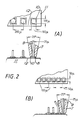
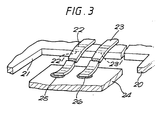
- Figure 3 illustrates a support member 20 defining a window 21.
- the support member 20 may be made of plastics or metal as explained above and a pair of electrically conductive ribbons 22, 23, for example Au, Al or Cu, are bonded to the support member 20.
- a silicon chip 24 having contacts 25, 26 is aligned with the bond positions on the support member and the ribbons are attached sequentially with ribbon 22 being first bonded to the support member 20 and then to contact 25 using the wire wedge bonding process. The ribbon is then broken off at this point from the supply and subsequently connected between the support member and pad 26 to form the ribbon 23.
- the ribbons 22, 23 are first bonded to the contacts 25, 26 on the silicon chip 24 using the wire wedge bonding technique and the free ends of the ribbons temporarily bonded to the support member 20.
- the method of ribbon or wire attachment for both the long and short term bonds may take the form of welding using ultrasonic energy or heat, soldering or adhesives.
- ultrasonic wedge bonding causes relatively less spread in the ribbons at the point of connection than with other forms of wire bonding.
- ribbons of gold, aluminium-1% silicon, or copper with ribbons nominally 30 ⁇ wide, the spreads with good bonding are of the order of 3-5 ⁇ , 4-7 ⁇ and 3-9 ⁇ , respectively.
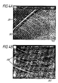
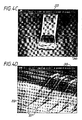
- Figure 4A illustrates a number of 25 micron diameter Al-1%Si wires 30 extending between a silicon surface 31 and PEEK material 32 which could constitute a suitable material for the support member 20.
- Figure 4B shows in more detail the bonding of 125 micron diameter wires 33 to a PPS substrate 34.
- Figure 4C illustrates the bonding of a ribbon 35 to polyimide tap 36.
- Figure 4D illustrates the bonding of ribbons 37 between silicon 38 and a PPS substrate 39.
- thermoset plastic base such as glass reinforced polyimide with a short glass fibre reinforced thermoplastic cover plate such as polyarylamide (PAM) can be used.
- PAM polyarylamide
- Figure 5A is a transverse section through the depending skirt of a cover plate, cap or lid prior to bonding.
- This skirt or contact edge of the cover plate is suitably shaped in cross section to provide a narrow projecting zone 40 together with adjoining recesses 41 to facilitate bonding of the plastics materials.
- the projection profile 40 serves as a so called energy concentrator, while the recesses 41 serve to retain the excess material (flash) squeezed out during the lid bonding operation.
- Figure 5B shows a pair of copper conductor ribbons 22, 23 mounted on a polyimide substrate constituting a support member 42, and held by a cover plate 43 which lies across the ribbons, the thermoplastic having become moulded around the conductors during the bonding operation to be in close contact with the substrate (thermoset plastic).
- thermoset plastic thermoplastic plastic
- the chip can be electrically tested at this point with the connecting leads mounted on the temporary substate.
- the chip 24 While coupled to the support member 20, the chip 24 can be handled for testing and the like without risk of damage. Finally, the ribbons 22, 23 are severed along lines 22′ and 23′ to release the chip 24 for subsequent attachment to a host device.
Landscapes
- Wire Bonding (AREA)
- Testing Of Individual Semiconductor Devices (AREA)
Applications Claiming Priority (2)
| Application Number | Priority Date | Filing Date | Title |
|---|---|---|---|
| GB898915816A GB8915816D0 (en) | 1989-07-11 | 1989-07-11 | Bonding electrical conductors |
| GB8915816 | 1989-07-11 |
Publications (2)
| Publication Number | Publication Date |
|---|---|
| EP0408272A2 true EP0408272A2 (fr) | 1991-01-16 |
| EP0408272A3 EP0408272A3 (en) | 1991-12-11 |
Family
ID=10659836
Family Applications (1)
| Application Number | Title | Priority Date | Filing Date |
|---|---|---|---|
| EP19900307447 Withdrawn EP0408272A3 (en) | 1989-07-11 | 1990-07-09 | Bonding electrical conductors |
Country Status (4)
| Country | Link |
|---|---|
| US (1) | US5054680A (fr) |
| EP (1) | EP0408272A3 (fr) |
| JP (1) | JPH0353536A (fr) |
| GB (1) | GB8915816D0 (fr) |
Cited By (1)
| Publication number | Priority date | Publication date | Assignee | Title |
|---|---|---|---|---|
| WO2004100258A3 (fr) * | 2003-05-02 | 2006-02-23 | Orthodyne Electronics Corp | Liaison de ruban |
Families Citing this family (6)
| Publication number | Priority date | Publication date | Assignee | Title |
|---|---|---|---|---|
| US5456404A (en) * | 1993-10-28 | 1995-10-10 | Digital Equipment Corporation | Method of testing semiconductor chips with reusable test package |
| US5894983A (en) * | 1997-01-09 | 1999-04-20 | Harris Corporation | High frequency, low temperature thermosonic ribbon bonding process for system-level applications |
| JPH11330134A (ja) * | 1998-05-12 | 1999-11-30 | Hitachi Ltd | ワイヤボンディング方法およびその装置並びに半導体装置 |
| US8614514B1 (en) | 2013-03-13 | 2013-12-24 | Palo Alto Research Center Incorporated | Micro-spring chip attachment using ribbon bonds |
| ITMI20131707A1 (it) * | 2013-10-15 | 2015-04-16 | Meccaniche Crizaf S P A Costruzioni | Dispositivo tenditore per nastro trasportatore |
| IT202000012379A1 (it) * | 2020-05-26 | 2021-11-26 | St Microelectronics Srl | Procedimento per fabbricare prodotti a semiconduttore, substrato, prodotto a semiconduttore e utensile corrispondenti |
Family Cites Families (5)
| Publication number | Priority date | Publication date | Assignee | Title |
|---|---|---|---|---|
| US4441248A (en) * | 1982-12-02 | 1984-04-10 | Stanley Electric Company, Ltd. | On-line inspection method and system for bonds made to electronic components |
| EP0117348B1 (fr) * | 1982-12-06 | 1987-03-11 | The Welding Institute | Procédé pour souder des fils aux composants semi-conducteurs |
| DE3543643A1 (de) * | 1985-12-11 | 1987-06-19 | Licentia Gmbh | Verfahren zum aufbringen eines ic auf ein substrat |
| US4979663A (en) * | 1986-08-27 | 1990-12-25 | Digital Equipment Corporation | Outer lead tape automated bonding system |
| DD266208A1 (de) * | 1987-10-30 | 1989-03-22 | Elektromat Veb | Verfahren zur ermittlung von fehlkontaktierungen bei der herstellung von halbleiteranordnungen |
-
1989
- 1989-07-11 GB GB898915816A patent/GB8915816D0/en active Pending
-
1990
- 1990-07-09 EP EP19900307447 patent/EP0408272A3/en not_active Withdrawn
- 1990-07-10 US US07/550,382 patent/US5054680A/en not_active Expired - Fee Related
- 1990-07-11 JP JP2181699A patent/JPH0353536A/ja active Pending
Cited By (3)
| Publication number | Priority date | Publication date | Assignee | Title |
|---|---|---|---|---|
| WO2004100258A3 (fr) * | 2003-05-02 | 2006-02-23 | Orthodyne Electronics Corp | Liaison de ruban |
| US8685791B2 (en) | 2003-05-02 | 2014-04-01 | Orthodyne Electronics Corporation | Ribbon bonding in an electronic package |
| US8685789B2 (en) | 2003-05-02 | 2014-04-01 | Orthodyne Electronics Corporation | Ribbon bonding in an electronic package |
Also Published As
| Publication number | Publication date |
|---|---|
| JPH0353536A (ja) | 1991-03-07 |
| GB8915816D0 (en) | 1989-08-31 |
| EP0408272A3 (en) | 1991-12-11 |
| US5054680A (en) | 1991-10-08 |
Similar Documents
| Publication | Publication Date | Title |
|---|---|---|
| US5795818A (en) | Integrated circuit chip to substrate interconnection and method | |
| US6344683B1 (en) | Stacked semiconductor package with flexible tape | |
| US6188127B1 (en) | Semiconductor packing stack module and method of producing the same | |
| EP0704895B1 (fr) | Procédé de fabrication d'un dispositif semi-conducteur et d'un substrat semi-conducteur | |
| EP0208494B1 (fr) | Procédé pour fabriquer un appareil semi-conducteur comprenant deux dispositifs semi-conducteurs | |
| US4949224A (en) | Structure for mounting a semiconductor device | |
| US5474957A (en) | Process of mounting tape automated bonded semiconductor chip on printed circuit board through bumps | |
| KR930010086B1 (ko) | 반도체 집적회로장치 | |
| KR950012658B1 (ko) | 반도체 칩 실장방법 및 기판 구조체 | |
| US6020629A (en) | Stacked semiconductor package and method of fabrication | |
| US4724472A (en) | Semiconductor device | |
| EP1005086B1 (fr) | Feuille métallique comprenant des plots de contact, substrat de circuit comprenant la feuille métallique, et dispositif sémiconducteur comprenant le substrat de circuit | |
| US6252178B1 (en) | Semiconductor device with bonding anchors in build-up layers | |
| KR20010069223A (ko) | 반도체 장치 및 그 제조 방법 | |
| WO1994024694A1 (fr) | Interconnexion d'une puce de circuit integree et d'un substrat | |
| JPH04277636A (ja) | 半導体装置とその製造方法及びこれに用いる接合体 | |
| US5661337A (en) | Technique for improving bonding strength of leadframe to substrate in semiconductor IC chip packages | |
| EP0482940B1 (fr) | Procédé de fabrication d'une connection électrique pour une puce de circuit intégré | |
| US5054680A (en) | Bonding electrical conductors | |
| US5704593A (en) | Film carrier tape for semiconductor package and semiconductor device employing the same | |
| US7198979B2 (en) | Method for manufacturing a stack arrangement of a memory module | |
| JPS59222947A (ja) | 半導体装置およびその製造方法 | |
| JP3508478B2 (ja) | 半導体装置の製造方法 | |
| US6624008B2 (en) | Semiconductor chip installing tape, semiconductor device and a method for fabricating thereof | |
| WO1987004010A1 (fr) | Assemblage mesa a interfaces de puces |
Legal Events
| Date | Code | Title | Description |
|---|---|---|---|
| PUAI | Public reference made under article 153(3) epc to a published international application that has entered the european phase |
Free format text: ORIGINAL CODE: 0009012 |
|
| AK | Designated contracting states |
Kind code of ref document: A2 Designated state(s): DE DK FR GB IT NL SE |
|
| PUAL | Search report despatched |
Free format text: ORIGINAL CODE: 0009013 |
|
| AK | Designated contracting states |
Kind code of ref document: A3 Designated state(s): DE DK FR GB IT NL SE |
|
| 17P | Request for examination filed |
Effective date: 19920610 |
|
| STAA | Information on the status of an ep patent application or granted ep patent |
Free format text: STATUS: THE APPLICATION HAS BEEN WITHDRAWN |
|
| 18W | Application withdrawn |
Withdrawal date: 19940317 |