EP0408797A1 - Dispositif de couplage pour signaux large bande - Google Patents
Dispositif de couplage pour signaux large bande Download PDFInfo
- Publication number
- EP0408797A1 EP0408797A1 EP89113373A EP89113373A EP0408797A1 EP 0408797 A1 EP0408797 A1 EP 0408797A1 EP 89113373 A EP89113373 A EP 89113373A EP 89113373 A EP89113373 A EP 89113373A EP 0408797 A1 EP0408797 A1 EP 0408797A1
- Authority
- EP
- European Patent Office
- Prior art keywords
- input
- driver circuit
- matrix
- line
- output
- Prior art date
- Legal status (The legal status is an assumption and is not a legal conclusion. Google has not performed a legal analysis and makes no representation as to the accuracy of the status listed.)
- Granted
Links
- 239000011159 matrix material Substances 0.000 claims abstract description 59
- 238000005516 engineering process Methods 0.000 claims abstract description 9
- 230000008878 coupling Effects 0.000 claims description 36
- 238000010168 coupling process Methods 0.000 claims description 36
- 238000005859 coupling reaction Methods 0.000 claims description 36
- 230000000903 blocking effect Effects 0.000 claims description 8
- 230000005540 biological transmission Effects 0.000 description 3
- 238000004891 communication Methods 0.000 description 3
- 230000000694 effects Effects 0.000 description 3
- 230000006399 behavior Effects 0.000 description 2
- 230000002411 adverse Effects 0.000 description 1
- 230000000295 complement effect Effects 0.000 description 1
- 238000011161 development Methods 0.000 description 1
- 230000018109 developmental process Effects 0.000 description 1
- 230000036039 immunity Effects 0.000 description 1
- 239000013307 optical fiber Substances 0.000 description 1
- 238000012856 packing Methods 0.000 description 1
- 230000000717 retained effect Effects 0.000 description 1
Images


Classifications
-
- H—ELECTRICITY
- H03—ELECTRONIC CIRCUITRY
- H03K—PULSE TECHNIQUE
- H03K19/00—Logic circuits, i.e. having at least two inputs acting on one output; Inverting circuits
- H03K19/0008—Arrangements for reducing power consumption
- H03K19/0016—Arrangements for reducing power consumption by using a control or a clock signal, e.g. in order to apply power supply
-
- H—ELECTRICITY
- H04—ELECTRIC COMMUNICATION TECHNIQUE
- H04Q—SELECTING
- H04Q3/00—Selecting arrangements
- H04Q3/42—Circuit arrangements for indirect selecting controlled by common circuits, e.g. register controller, marker
- H04Q3/52—Circuit arrangements for indirect selecting controlled by common circuits, e.g. register controller, marker using static devices in switching stages, e.g. electronic switching arrangements
- H04Q3/521—Circuit arrangements for indirect selecting controlled by common circuits, e.g. register controller, marker using static devices in switching stages, e.g. electronic switching arrangements using semiconductors in the switching stages
Definitions
- narrowband and broadband communication services which provide optical fibers as a transmission medium in the area of subscriber lines, via which both narrowband communication services, such as 64 kbit / s digital telephony in particular, as well as broadband communication services, such as 140 Mbit / s video telephony in particular, whereby the switching centers (preferably having common control devices) can also provide narrowband signal coupling devices and broadband signal coupling devices side by side (DE-PS 24 21 002).
- a broadband signal coupling device known has a crosspoint matrix in FET technology, the coupling elements of which each have a switching electrode or blocking signal applied to their control electrode and a main electrode connected to the associated matrix output line Switch transistor are formed, the coupling elements each having a series circuit with the switch transistor ballast transistor, which is connected with its control electrode to the associated matrix input line and whose main electrode facing away from the series circuit via a scanning transistor with one connection of the Operating voltage source is connected, the other connection of which the respective matrix output line is connected via a precharge transistor, and wherein precharge transistor and sense transistor are mutually opposed to one another at their control electrode with a one-bit switching period in one Precharge phase and the actual switching phase dividing switching matrix drive clock are applied, so that in each pre-phase when the scanning transistor is blocked, the matrix output line via the precharge transistor is at least approximated to that of the other ren connection of the operating voltage source prevailing potential is charged.
- This known broadband signal coupling device which can have coupling element-individual scanning transistors or matrix input line or matrix output line-individual scanning transistors, requires its own clock lines which pull through the crosspoint matrix to control these scanning transistors, which requires a corresponding area requirement and a corresponding capacitive load on the matrix output lines brings with it; Clock distribution and couplings between matrix input lines and matrix output lines require sufficiently large signal amplitudes on the matrix output lines to ensure sufficient interference immunity, which is associated with a relatively high power consumption.
- the main electrode of the other transistor of each coupling element facing away from the series circuit is connected to the one connection of the operating voltage source via a matrix output line individual transistor connected at its control electrode to the output of a matrix output line-individual output amplifier circuit; in the event of a signal state change at the output of the output amplifier circuit, this transistor is blocked and thus a further charge reversal of the output line is avoided, which limits the signal swing on the output line.
- the object of the invention is to provide a broadband signal coupling device with limitation of the signal swing on the input lines.
- the invention relates to a broadband signal coupling device with a crosspoint matrix in FET technology, the inputs of which are each provided with an input driver circuit and the outputs of which can each be provided with an output driver circuit, the matrix output lines in each case via a precharge circuit which is provided with a Bit switching period in a precharge phase and the actual switching phase dividing clock signal is controlled, can be charged in each precharge phase to a precharge potential lying between the two operating potentials or to one of the two operating potentials themselves;
- This broadband signal coupling device is characterized according to the invention in that the output of the respective input driver circuit is connected via a feedback element with a threshold value to a lock input of the input driver circuit, via which the transfer of the output of the relevant input driver circuit is terminated.
- the invention has the advantage of strictly limiting the signal swing on the input lines.
- the reduction in the signal swing on the input lines leads to a reduction in the charge-reversal losses, which is synonymous with a reduced current consumption.
- the reduced current consumption is accompanied by a correspondingly reduced power loss, which allows an increase in the packing density of coupling elements or the switching frequency.
- the reduced current consumption results in a reduction in disturbances in the operating voltage of the broadband signal coupling device caused by current peaks.
- the signal stroke limitation results in a reduction in adverse influences on adjacent signal paths.
- the input driver circuit can be formed with an inverter amplifier, in whose operating voltage connection a transistor is inserted, the control electrode of which forms the blocking input of the input driver circuit. This configuration allows the input driver circuit to be designed with particularly little effort.
- the input driver circuit is expediently constructed using CMOS technology. This measure makes the input driver circuit particularly easy to control.
- the feedback element can be formed with a number of CMOS inverter amplifiers.
- the feedback element is implemented in the same technology as the rest of the crosspoint matrix and can therefore be easily integrated.
- the switching threshold of such a feedback element formed with CMOS inverter amplifiers depends on the switching threshold of the first CMOS inverter amplifier and is typically 40% of the operating voltage feeding the feedback element.
- the feedback element consists of two CMOS inverter amplifiers. That’s it Output signal of the feedback element in phase with the input signal of the feedback element.
- the feedback element can be formed with a comparator, one input of which is supplied with a reference voltage and the other input of which is the output signal of the respective input driver circuit.
- This embodiment allows the threshold voltage to be set to a specific value.
- the feedback element in turn is also possible for the feedback element in turn to be fed back via a high-resistance resistor.
- this measure increases the gain in the area of the switching threshold of the feedback element and, on the other hand, causes a small switching hysteresis. Both effects improve the switching behavior of the feedback element.
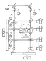
- FIG 1 is schematically outlined in the scope necessary for understanding the invention, a broadband signal coupling device, the input lines el ... ej each via gate circuits Gl ... Gj, which are controlled by a common clock signal T PC , and input driver circuits El ... Ej with (matrix input lines) column lines sl ... sj of the crosspoint matrix and these in turn are connected via column-specific feedback elements Rl ... Rj to a lock input s' of the associated input driver circuit E.
- the (matrix input lines) row lines zl..zm the crosspoint matrix are on the one hand with row-specific precharge circuits PCl ... PCm, which are controlled by a common clock signal T PC , and on the other hand via output driver circuits Al ... Am with latches (latches) Ll ... Lm connected, which in turn are controlled by a common clock signal T PC .
- the crosspoint matrix has crosspoints KPll ... KPmj, the coupling elements of which, as is further indicated in detail for the coupling point KPij for its coupling element Kij, can each be controlled by a crosspoint-specific holding memory cell Hij (at the coupling point KPij), the output of which r leads to the control input r of the respective coupling element (Kij at the coupling point KPij).
- the hold memory cells ... Hij ... are, according to FIG. 1, by two control decoders, namely a row decoder DX and a column decoder DY, via corresponding control lines xl ... xm; yl ... yj controlled in two coordinates.
- the two control decoders DX, DY from input registers Reg X, Reg Y can each be loaded with a crosspoint row or crosspoint column address common to a matrix row (row or column) of crosspoints which each emit a "1" control signal on the control line corresponding to the respective crosspoint row address.
- the coincidence of a row drive signal "1" and a column drive signal "1" at the intersection of the relevant matrix row with the relevant matrix column when a corresponding connection is established then causes the holding memory cell located there, for example the memory cell Hij, to be activated, with the result that the relevant holding memory cell (Hij) controlled coupling element, in the example the coupling element Kij, becomes conductive.
- the control decoder DX is again acted upon by the input register Reg X with the relevant line address, so that the line decoder DX again outputs a line control signal "1" on its output line xi, and at the same time, the column decoder DY is loaded from its input register Reg Y, for example with an empty address or with the address of a column of non-connected crosspoints, so that it outputs a column drive signal "0" on its output line yj; the coincidence of row drive signal "1" and column drive signal "0” then causes the hold memory cell Hij to be reset, with the result that the coupling element Kij controlled by it is blocked.
- the holding memory cells ... Hij ... can be designed in a manner known per se; for example, the hold memory cells, e.g. Known from EP-A-0 238 834 and also outlined in FIG 2, with an n-channel transistor Tnh and two cross-coupled inverter circuits (CMOS inverter circuits Tp ', Tn'; Tp ⁇ , Tn ⁇ be formed, an inverter circuit is connected on the input side to the associated decoder output yj of one drive decoder via the n-channel transistor Tnh, which in turn has the control signal applied to the output signal of the associated decoder output xi of the other drive decoder at its control electrode, and an inverter circuit on the output side leads to the control input r of the associated coupling element .
- CMOS inverter circuits Tp ', Tn'; Tp ⁇ , Tn ⁇ cross-coupled inverter circuits
- FIG. 3 illustrates how the coupling elements ... Kij ... can be implemented in terms of circuitry:
- the coupling elements ... Kij ... are each connected in series with one of its control electrodes from the holding memory cell with a switch-through or Switching signal applied to switch transistor Tk and an input transistor Te connected with its control electrode to the associated (matrix input line) column line sj, which is connected to the main electrode of a transistor Tk facing away from the series circuit associated (matrix output line) row line zi is connected.
- the (matrix output line) row line zi is connected via a precharge circuit PC to a precharge potential source, from which the (matrix output line) row line zi can be charged to a precharge potential lying between the two operating potentials or to one of the two operating potentials itself.
- a precharge potential source for a precharge potential lying between the two operating potentials can be formed in particular in a manner known in principle (for example from EP-A-0 249 837) with a feedback CMOS inverter, via which the row line is at least approximated in each case in a precharge phase of a bit switching period is charged to the potential corresponding to the switching threshold of the inverter.
- a feedback CMOS inverter via which the row line is at least approximated in each case in a precharge phase of a bit switching period is charged to the potential corresponding to the switching threshold of the inverter.
- the (matrix output line) row line zi is connected to the one connection (U DD ) of the operating voltage source U DD -U SS via a precharge circuit which, as can also be seen from FIG. known from EP-A-0 262 479) is formed with a precharge transistor Tipc with its control electrode on a precharge clock line T PC .
- the main electrode of the other transistor Te facing away from the series circuit is connected continuously, ie not clock-controlled, to the other connection (U SS , ground) of the operating voltage source U DD -U SS .
- FIG. 4 illustrates how the input driver circuits El ... Ej can be implemented in terms of circuitry:
- the input driver circuit E according to FIG. 4 is constructed with a CMOS inverter amplifier, formed with two transistors T2, T3, one of which has an operating voltage connection directly with the operating voltage source U DD -U SS and its other operating voltage connection is connected via a transistor T1 to the operating voltage source U DD -U SS .
- the control electrode of transistor T1 forms the blocking input s' of the input amplifier kers E
- the connection of the control electrodes of the transistors T2 and T3 form the input e 'of the input driver circuit E
- the connection of the main electrodes of the transistors T2 and T3 form the output of the input driver circuit E, which is connected to the respective column line s.
- FIG. 5 shows how the feedback elements Rl... Rj with threshold values can be implemented in terms of circuitry:
- the feedback elements Rl ... Rj are formed here with a chain connection of two CMOS inverters IN1, IN2, the respective column line s being connected to the control electrodes of the complementary transistor pair forming the first CMOS inverter IN1 and the connection point of the main electrodes of the first transistor pair is connected to the control electrodes of the transistor pair forming the second CMOS inverter IN2.
- the connection of the two main electrodes of the second pair of transistors forms the output s' of the respective feedback element Rl ... Rj.
- the characteristic switching threshold of such a feedback element R formed with CMOS inverters IN1, IN2 depends on the threshold voltage U TH of the first inverter IN1 and is approximately 40% of the operating voltage feeding the feedback element R. Accordingly, the switching threshold for the feedback element R according to FIG. 5 is approximately 2V for an operating voltage U DD -U SS of 5V.
- the feedback element R can be formed in accordance with FIG. 6 with a comparator KOMP, as can be provided, for example, by an operational amplifier, the non-inverting input (+) of which is connected to the respective ( Matrix input line) is connected to column line s and its inverting input (-) is connected to one terminal of a reference voltage source UR, the other terminal of which is connected to a terminal of the operating voltage source U DD -U SS .
- the output of the comparator KOMP forms the connection for the lock input s' of the input driver scarf device E.
- the switching threshold U TH of such a feedback element R corresponds to the voltage level at the inverting input (-) of the comparator KOMP.
- the feedback elements R according to FIG. 5 or FIG. 6 can in turn be fed back by means of a high-resistance resistor W, which connects the output s' to the input s of the feedback element R and which on the one hand increases the gain in the area of the switching threshold and on the other hand has a small hysteresis of the switching threshold causes. Both effects improve the switching behavior of the feedback element R.
- the output driver circuits Al ... Am can in principle be constructed in the same way as the feedback elements R according to FIG. 5.
- the latches Ll ... Lm forming the output of the crosspoint matrix are sufficiently known and therefore do not need to be described in more detail here.
- FIG. 7 shows the transmission of a "HIGH” signal and then a "LOW" signal (see line e) for two successive bit switching periods, for example from an input ej (in FIG. 1) to an output ai (in FIG. 1 ) of the crosspoint matrix (FIG. 1):
- a corresponding clock signal T PC (line T PC in FIG. 7), which acts on the control electrode of each precharging transistor (Tipc in FIG. 3) (line T PC in FIG. 7), has the effect that in each precharging phase pv (in FIG. below) of a bit period divided by the clock signal T PC into such a precharge phase pv and a subsequent main phase (ph in FIG. 7) of each precharge transistor (Tipc in FIG. 3), so that during the precharge phase pv the (matrix output lines) Row lines zl ... zm are charged via the respective precharge transistor (Tipc) to a precharge potential lying between the two operating potentials or to one of the two operating potentials themselves (cf. FIG. 7, line z, a, dash-dot line) .
- the precharge transistors Tipc are blocked in the example by a "HIGH" clock signal T PC (see FIG. 7, line T PC ); at the same time, the gate inputs Gl ... Gj on the matrix input side are unlocked.
- the signals applied to the input lines of the crosspoint matrix el ... ej are in the example inverted through to the input e 'of the respective input driver circuit E.
- a "HIGH" signal, for example, applied to the input line ej (cf. FIG. 7, line e) thus causes a "LOW" signal at the input ej 'of the input driver circuit Ej (cf. FIG 7, line e').
- the input driver circuit E charges the (matrix input line) column line s connected to a signal at the input e 'of the input driver circuit E (in the example “LOW”) signal (FIG. 7, line s) until the charge flow through Blocking the transistor T1 (in FIG 4) is interrupted.
- a suitable for blocking the transistor T1, in the example "HIGH” signal is emitted by a feedback element R according to FIG. 5 or according to FIG. 6, the input of which is connected to the respective (matrix input line) column line s and reaches a predetermined threshold voltage U TH (see FIG. 7, line s, s')
- the threshold voltage U TH is dimensioned in such a way that the input transistors (Te in FIG. 3) connected to its control electrode with the respective (matrix input line) column line s are reliably switched on. If the switching transistor Tk (in FIG. 3) is conductive in a coupling element Kij (in FIG. 3) at the control input r ("HIGH") switching signal (see FIG. 7, line r), and thus the coupling point KPij is in the switching state, Thus, the (line output line) row line z connected via the switched coupling element Kij to the (matrix input line) column line s via the transistors Te and Tk becomes a potential of the operating voltage source U DD -U SS (in the example U SS , ground ) discharge.
- a signal state present on the relevant (matrix input line) column line s is inverted through the respective coupling point unlocked from its control input r (cf. FIG. 7, line s; z, a).
- the "LOW" signal present at the output ai of the output driver circuit Ai becomes, for example, with the signal change of the pre-data clock signal leading from the "HIGH” state to the "L0W” state T PC transferred into the associated latch Li, the gate circuits Gl ... Gj are locked, ie "HIGH” signals are present at all inputs e 'of the input driver circuits E, as a result of which all transistors T3 (in FIG. 4) are switched to conductive and thereby all (matrix input lines) column lines sl..sj are discharged (cf. FIG. 7, line s), the feedback elements R return to the basic state (in the example "LOW” state) (cf. FIG. 7, line s '), The transistors T1 (in FIG 4) are switched on.
- a "LOW" signal should now be transmitted in the subsequent bit switching period via the input line ej in question.
- all (matrix output lines) row lines zl ... zm are preloaded again.
- the switching transistor T k in the crosspoint under consideration may again be in the on state due to a (in the example "HIGH") control signal r (cf. FIG. 7, line r). Since a "LOW" signal is present on the input line ej (see line e in FIG. 7), the associated (matrix input line) column line sj also remains in the "LOW” state, with the result that the input transistor Te is in the crosspoint under consideration (see FIG. 3) remains blocked, the associated (matrix output line) row line zi is not discharged and, the signal state on the output line ai in question is retained (see FIG. 7, row z, a); at the end of this main phase ph, a "HIGH" signal is therefore transferred to the latch Li.
- a "HIGH" signal is therefore transferred to the latch Li.
Landscapes
- Engineering & Computer Science (AREA)
- Computer Networks & Wireless Communication (AREA)
- Physics & Mathematics (AREA)
- Computer Hardware Design (AREA)
- Computing Systems (AREA)
- General Engineering & Computer Science (AREA)
- Mathematical Physics (AREA)
- Electronic Switches (AREA)
- Use Of Switch Circuits For Exchanges And Methods Of Control Of Multiplex Exchanges (AREA)
- Amplifiers (AREA)
- Control Of Motors That Do Not Use Commutators (AREA)
- Medicines That Contain Protein Lipid Enzymes And Other Medicines (AREA)
- Polarising Elements (AREA)
- Control Of Indicators Other Than Cathode Ray Tubes (AREA)
- Measurement And Recording Of Electrical Phenomena And Electrical Characteristics Of The Living Body (AREA)
- Measuring Pulse, Heart Rate, Blood Pressure Or Blood Flow (AREA)
- Liquid Crystal Display Device Control (AREA)
- Filters And Equalizers (AREA)
- Input Circuits Of Receivers And Coupling Of Receivers And Audio Equipment (AREA)
Priority Applications (8)
| Application Number | Priority Date | Filing Date | Title |
|---|---|---|---|
| DE89113373T DE58906841D1 (de) | 1989-07-20 | 1989-07-20 | Breitbandsignal-Koppeleinrichtung. |
| AT89113373T ATE100988T1 (de) | 1989-07-20 | 1989-07-20 | Breitbandsignal-koppeleinrichtung. |
| EP89113373A EP0408797B1 (fr) | 1989-07-20 | 1989-07-20 | Dispositif de couplage pour signaux large bande |
| LU87689A LU87689A1 (de) | 1989-07-20 | 1990-02-23 | Breitbandsignal-koppeleinrichtung |
| JP2188179A JPH03219794A (ja) | 1989-07-20 | 1990-07-18 | 広帯域信号結合装置 |
| CA002021468A CA2021468A1 (fr) | 1989-07-20 | 1990-07-18 | Reseau de commutation de signaux a large bande |
| HU904550A HU207631B (en) | 1989-07-20 | 1990-07-19 | Broad band signal switching device |
| SU904830384A RU2013877C1 (ru) | 1989-07-20 | 1990-07-20 | Устройство связи широкополосных сигналов |
Applications Claiming Priority (1)
| Application Number | Priority Date | Filing Date | Title |
|---|---|---|---|
| EP89113373A EP0408797B1 (fr) | 1989-07-20 | 1989-07-20 | Dispositif de couplage pour signaux large bande |
Publications (2)
| Publication Number | Publication Date |
|---|---|
| EP0408797A1 true EP0408797A1 (fr) | 1991-01-23 |
| EP0408797B1 EP0408797B1 (fr) | 1994-01-26 |
Family
ID=8201657
Family Applications (1)
| Application Number | Title | Priority Date | Filing Date |
|---|---|---|---|
| EP89113373A Expired - Lifetime EP0408797B1 (fr) | 1989-07-20 | 1989-07-20 | Dispositif de couplage pour signaux large bande |
Country Status (8)
| Country | Link |
|---|---|
| EP (1) | EP0408797B1 (fr) |
| JP (1) | JPH03219794A (fr) |
| AT (1) | ATE100988T1 (fr) |
| CA (1) | CA2021468A1 (fr) |
| DE (1) | DE58906841D1 (fr) |
| HU (1) | HU207631B (fr) |
| LU (1) | LU87689A1 (fr) |
| RU (1) | RU2013877C1 (fr) |
Families Citing this family (1)
| Publication number | Priority date | Publication date | Assignee | Title |
|---|---|---|---|---|
| US6998935B2 (en) * | 2003-02-19 | 2006-02-14 | M/A-Com, Inc. | Switch matrix |
Citations (3)
| Publication number | Priority date | Publication date | Assignee | Title |
|---|---|---|---|---|
| EP0103236A2 (fr) * | 1982-09-13 | 1984-03-21 | Kabushiki Kaisha Toshiba | Circuit logique |
| EP0219701A2 (fr) * | 1985-10-19 | 1987-04-29 | Richard Hirschmann GmbH & Co. | Circuit comparateur |
| EP0262479A1 (fr) * | 1986-09-17 | 1988-04-06 | Siemens Aktiengesellschaft | Dispositif de commutation pour signaux à large bande |
-
1989
- 1989-07-20 AT AT89113373T patent/ATE100988T1/de active
- 1989-07-20 EP EP89113373A patent/EP0408797B1/fr not_active Expired - Lifetime
- 1989-07-20 DE DE89113373T patent/DE58906841D1/de not_active Expired - Fee Related
-
1990
- 1990-02-23 LU LU87689A patent/LU87689A1/de unknown
- 1990-07-18 JP JP2188179A patent/JPH03219794A/ja active Pending
- 1990-07-18 CA CA002021468A patent/CA2021468A1/fr not_active Abandoned
- 1990-07-19 HU HU904550A patent/HU207631B/hu not_active IP Right Cessation
- 1990-07-20 RU SU904830384A patent/RU2013877C1/ru active
Patent Citations (3)
| Publication number | Priority date | Publication date | Assignee | Title |
|---|---|---|---|---|
| EP0103236A2 (fr) * | 1982-09-13 | 1984-03-21 | Kabushiki Kaisha Toshiba | Circuit logique |
| EP0219701A2 (fr) * | 1985-10-19 | 1987-04-29 | Richard Hirschmann GmbH & Co. | Circuit comparateur |
| EP0262479A1 (fr) * | 1986-09-17 | 1988-04-06 | Siemens Aktiengesellschaft | Dispositif de commutation pour signaux à large bande |
Non-Patent Citations (2)
| Title |
|---|
| PATENT ABSTRACTS OF JAPAN, Band 8, Nr. 261 (E-281)[1698], 30. November 1984; & JP-A-59 131 221 (NIHON DENKI AISHII MAIKON SYSTEM K.K.) * |
| PATENT ABSTRACTS OF JAPAN, Band 9, Nr. 302 (E-362)[2025], 29. November 1985; & JP-A-60 139 020 (TOSHIBA) 23-07-1985 * |
Also Published As
| Publication number | Publication date |
|---|---|
| HU904550D0 (en) | 1990-12-28 |
| DE58906841D1 (de) | 1994-03-10 |
| RU2013877C1 (ru) | 1994-05-30 |
| EP0408797B1 (fr) | 1994-01-26 |
| ATE100988T1 (de) | 1994-02-15 |
| LU87689A1 (de) | 1990-07-24 |
| HUT54445A (en) | 1991-02-28 |
| CA2021468A1 (fr) | 1991-01-21 |
| JPH03219794A (ja) | 1991-09-27 |
| HU207631B (en) | 1993-04-28 |
Similar Documents
| Publication | Publication Date | Title |
|---|---|---|
| EP0262479B1 (fr) | Dispositif de commutation pour signaux à large bande | |
| EP0264046B1 (fr) | Dispositif de commutation pour signaux à large bande | |
| EP0345623B1 (fr) | Dispositif de commutation pour signaux à large bande | |
| DE2802595C2 (de) | Schaltungsanordnung mit Feldeffekttransistoren zur Spannungspegelumsetzung | |
| EP0238834A1 (fr) | Dispositif de couplage spatial pour signaux à large bande | |
| EP0249836B1 (fr) | Dispositif de commutation pour signaux à large bande | |
| EP0408797B1 (fr) | Dispositif de couplage pour signaux large bande | |
| EP0249837B1 (fr) | Dispositif de commutation pour signaux à large bande | |
| EP0451312B1 (fr) | Dispositif de commutation pour signaux à large bande | |
| EP0354252B1 (fr) | Dispositif de couplage pour signaux à large bande | |
| EP0389663B1 (fr) | Dispositif de commutation pour signaux à large bande | |
| EP0417336B1 (fr) | Dispositif de commutation pour signaux à large bande | |
| EP0477403B1 (fr) | Dispositif de couplage de signaux à bande large avec un circuit de transfert de charge dans des lignes de sortie | |
| EP0311956B1 (fr) | Dispositif de couplage pour signaux large bande | |
| EP0354253B1 (fr) | Dispositif de couplage pour signaux à large bande | |
| EP0217203B1 (fr) | Dispositif de couplage spatial pour signaux à large bande | |
| EP0354254B1 (fr) | Dispositif de couplage pour signaux à large bande | |
| EP0905892A2 (fr) | Bascule RS avec des entrées de validation | |
| EP0388856B1 (fr) | Dispositif de couplage pour signaux à large bande | |
| DE3604607A1 (de) | Breitbandsignal-raumkoppeleinrichtung | |
| DE2348453C3 (de) | Koppelmatrix mit für sich bistabilen Koppelpunkten | |
| DE3734822A1 (de) | Breitbandsignal-koppeleinrichtung |
Legal Events
| Date | Code | Title | Description |
|---|---|---|---|
| PUAI | Public reference made under article 153(3) epc to a published international application that has entered the european phase |
Free format text: ORIGINAL CODE: 0009012 |
|
| AK | Designated contracting states |
Kind code of ref document: A1 Designated state(s): AT BE CH DE FR GB IT LI NL SE |
|
| 17P | Request for examination filed |
Effective date: 19901220 |
|
| 17Q | First examination report despatched |
Effective date: 19930408 |
|
| GRAA | (expected) grant |
Free format text: ORIGINAL CODE: 0009210 |
|
| AK | Designated contracting states |
Kind code of ref document: B1 Designated state(s): AT BE CH DE FR GB IT LI NL SE |
|
| REF | Corresponds to: |
Ref document number: 100988 Country of ref document: AT Date of ref document: 19940215 Kind code of ref document: T |
|
| REF | Corresponds to: |
Ref document number: 58906841 Country of ref document: DE Date of ref document: 19940310 |
|
| ITF | It: translation for a ep patent filed | ||
| GBT | Gb: translation of ep patent filed (gb section 77(6)(a)/1977) |
Effective date: 19940407 |
|
| ET | Fr: translation filed | ||
| PLBE | No opposition filed within time limit |
Free format text: ORIGINAL CODE: 0009261 |
|
| STAA | Information on the status of an ep patent application or granted ep patent |
Free format text: STATUS: NO OPPOSITION FILED WITHIN TIME LIMIT |
|
| 26N | No opposition filed | ||
| EAL | Se: european patent in force in sweden |
Ref document number: 89113373.8 |
|
| PGFP | Annual fee paid to national office [announced via postgrant information from national office to epo] |
Ref country code: GB Payment date: 19970620 Year of fee payment: 9 Ref country code: AT Payment date: 19970620 Year of fee payment: 9 |
|
| PGFP | Annual fee paid to national office [announced via postgrant information from national office to epo] |
Ref country code: BE Payment date: 19970710 Year of fee payment: 9 |
|
| PGFP | Annual fee paid to national office [announced via postgrant information from national office to epo] |
Ref country code: SE Payment date: 19970711 Year of fee payment: 9 |
|
| PGFP | Annual fee paid to national office [announced via postgrant information from national office to epo] |
Ref country code: NL Payment date: 19970714 Year of fee payment: 9 |
|
| PGFP | Annual fee paid to national office [announced via postgrant information from national office to epo] |
Ref country code: FR Payment date: 19970718 Year of fee payment: 9 |
|
| PGFP | Annual fee paid to national office [announced via postgrant information from national office to epo] |
Ref country code: CH Payment date: 19971028 Year of fee payment: 9 |
|
| PG25 | Lapsed in a contracting state [announced via postgrant information from national office to epo] |
Ref country code: GB Free format text: LAPSE BECAUSE OF NON-PAYMENT OF DUE FEES Effective date: 19980720 Ref country code: AT Free format text: LAPSE BECAUSE OF NON-PAYMENT OF DUE FEES Effective date: 19980720 |
|
| PG25 | Lapsed in a contracting state [announced via postgrant information from national office to epo] |
Ref country code: SE Free format text: LAPSE BECAUSE OF NON-PAYMENT OF DUE FEES Effective date: 19980721 |
|
| PG25 | Lapsed in a contracting state [announced via postgrant information from national office to epo] |
Ref country code: LI Free format text: LAPSE BECAUSE OF NON-PAYMENT OF DUE FEES Effective date: 19980731 Ref country code: CH Free format text: LAPSE BECAUSE OF NON-PAYMENT OF DUE FEES Effective date: 19980731 Ref country code: BE Free format text: LAPSE BECAUSE OF NON-PAYMENT OF DUE FEES Effective date: 19980731 |
|
| PGFP | Annual fee paid to national office [announced via postgrant information from national office to epo] |
Ref country code: DE Payment date: 19980917 Year of fee payment: 10 |
|
| BERE | Be: lapsed |
Owner name: SIEMENS A.G. Effective date: 19980731 |
|
| PG25 | Lapsed in a contracting state [announced via postgrant information from national office to epo] |
Ref country code: NL Free format text: LAPSE BECAUSE OF NON-PAYMENT OF DUE FEES Effective date: 19990201 |
|
| GBPC | Gb: european patent ceased through non-payment of renewal fee |
Effective date: 19980720 |
|
| REG | Reference to a national code |
Ref country code: CH Ref legal event code: PL |
|
| EUG | Se: european patent has lapsed |
Ref document number: 89113373.8 |
|
| PG25 | Lapsed in a contracting state [announced via postgrant information from national office to epo] |
Ref country code: FR Free format text: LAPSE BECAUSE OF NON-PAYMENT OF DUE FEES Effective date: 19990331 |
|
| NLV4 | Nl: lapsed or anulled due to non-payment of the annual fee |
Effective date: 19990201 |
|
| REG | Reference to a national code |
Ref country code: FR Ref legal event code: ST |
|
| PG25 | Lapsed in a contracting state [announced via postgrant information from national office to epo] |
Ref country code: DE Free format text: LAPSE BECAUSE OF NON-PAYMENT OF DUE FEES Effective date: 20000503 |
|
| APCB | Communication from the board of appeal sent |
Free format text: ORIGINAL CODE: EPIDOS OBAPE |
|
| PG25 | Lapsed in a contracting state [announced via postgrant information from national office to epo] |
Ref country code: IT Free format text: LAPSE BECAUSE OF NON-PAYMENT OF DUE FEES Effective date: 20050720 |