EP0409041A1 - Méthode pour la formation d'un oxyde de base épais dans un procédé BICMOS - Google Patents
Méthode pour la formation d'un oxyde de base épais dans un procédé BICMOS Download PDFInfo
- Publication number
- EP0409041A1 EP0409041A1 EP90113112A EP90113112A EP0409041A1 EP 0409041 A1 EP0409041 A1 EP 0409041A1 EP 90113112 A EP90113112 A EP 90113112A EP 90113112 A EP90113112 A EP 90113112A EP 0409041 A1 EP0409041 A1 EP 0409041A1
- Authority
- EP
- European Patent Office
- Prior art keywords
- region
- bipolar
- dielectric
- conductivity type
- emitter
- Prior art date
- Legal status (The legal status is an assumption and is not a legal conclusion. Google has not performed a legal analysis and makes no representation as to the accuracy of the status listed.)
- Granted
Links
Images


Classifications
-
- H—ELECTRICITY
- H10—SEMICONDUCTOR DEVICES; ELECTRIC SOLID-STATE DEVICES NOT OTHERWISE PROVIDED FOR
- H10D—INORGANIC ELECTRIC SEMICONDUCTOR DEVICES
- H10D10/00—Bipolar junction transistors [BJT]
- H10D10/01—Manufacture or treatment
- H10D10/051—Manufacture or treatment of vertical BJTs
-
- H—ELECTRICITY
- H10—SEMICONDUCTOR DEVICES; ELECTRIC SOLID-STATE DEVICES NOT OTHERWISE PROVIDED FOR
- H10D—INORGANIC ELECTRIC SEMICONDUCTOR DEVICES
- H10D84/00—Integrated devices formed in or on semiconductor substrates that comprise only semiconducting layers, e.g. on Si wafers or on GaAs-on-Si wafers
- H10D84/01—Manufacture or treatment
- H10D84/0107—Integrating at least one component covered by H10D12/00 or H10D30/00 with at least one component covered by H10D8/00, H10D10/00 or H10D18/00, e.g. integrating IGFETs with BJTs
- H10D84/0109—Integrating at least one component covered by H10D12/00 or H10D30/00 with at least one component covered by H10D8/00, H10D10/00 or H10D18/00, e.g. integrating IGFETs with BJTs the at least one component covered by H10D12/00 or H10D30/00 being a MOS device
-
- H—ELECTRICITY
- H10—SEMICONDUCTOR DEVICES; ELECTRIC SOLID-STATE DEVICES NOT OTHERWISE PROVIDED FOR
- H10D—INORGANIC ELECTRIC SEMICONDUCTOR DEVICES
- H10D84/00—Integrated devices formed in or on semiconductor substrates that comprise only semiconducting layers, e.g. on Si wafers or on GaAs-on-Si wafers
- H10D84/01—Manufacture or treatment
- H10D84/02—Manufacture or treatment characterised by using material-based technologies
- H10D84/03—Manufacture or treatment characterised by using material-based technologies using Group IV technology, e.g. silicon technology or silicon-carbide [SiC] technology
- H10D84/038—Manufacture or treatment characterised by using material-based technologies using Group IV technology, e.g. silicon technology or silicon-carbide [SiC] technology using silicon technology, e.g. SiGe
-
- H—ELECTRICITY
- H10—SEMICONDUCTOR DEVICES; ELECTRIC SOLID-STATE DEVICES NOT OTHERWISE PROVIDED FOR
- H10D—INORGANIC ELECTRIC SEMICONDUCTOR DEVICES
- H10D84/00—Integrated devices formed in or on semiconductor substrates that comprise only semiconducting layers, e.g. on Si wafers or on GaAs-on-Si wafers
- H10D84/40—Integrated devices formed in or on semiconductor substrates that comprise only semiconducting layers, e.g. on Si wafers or on GaAs-on-Si wafers characterised by the integration of at least one component covered by groups H10D12/00 or H10D30/00 with at least one component covered by groups H10D10/00 or H10D18/00, e.g. integration of IGFETs with BJTs
- H10D84/401—Combinations of FETs or IGBTs with BJTs
Definitions
- This invention is in the field of integrated circuits, and is specifically directed to methods of fabricating bipolar and CMOS transistors in the same integrated circuit.
- BiCMOS complementary MOS
- BiCMOS devices may of course be accomplished by forming the bipolar transistors according to known techniques in selected areas of the device, by forming the MOS transistors according to known techniques in selected areas of the device, and interconnecting the two types of transistors.
- certain features of each type of transistor tend to be incompatible, from a process standpoint, with the other type, requiring a large number of process steps to form each. It is therefore preferable in the manufacture of such BiCMOS circuits to utilize structures which are useful in both types of transistors, in order to minimize the process complexity and cost.
- Such dual utilization of structural components and process steps generally results in a process which is less than optimal for either the bipolar or the MOS transistors, or both.
- Prior methods for forming the bipolar transistors in such structures have incorporated thin oxide layers between the diffused base region and the overlying emitter electrode (generally formed of polysilicon).
- the thin oxide over the base is generally formed in the same step as the gate oxide for the MOS transistors, and therefore is generally of a thickness on the order of 20nm.
- Such thin oxides separating the base region from the emitter electrode cause certain problems, however. Firstly, performance of the bipolar transistors degrades as the emitter-to-base capacitance increases. Of course, such capacitance increases as the dielectric thickness therebetween decreases, making it preferable to have a thicker dielectric between the emitter and the base region. In addition, a thin dielectric between the emitter electrode and the base region is inherently weaker to stress from subsequent processing steps such as contact etch, silicidation, and metal deposition and sinter. Furthermore, a thin dielectric also increases the risk that a contact via formed over the oxide for connecting an overlying metallization layer to the emitter electrode will leak to the base region.
- the dielectric under the emitter electrode will be further thinned, in turn further increasing the emitter-to-base capacitance.
- the dielectric may be etched completely through, shorting the overlying metal and the emitter electrode to the base region.
- the method described in said copending application S.N. 366,224 describes the formation of a bipolar transistor in a BiCMOS process where the same polysilicon layer is used to form the emitter and gate electrodes, but where a thicker base oxide is provided under the emitter electrode than under the gate electrodes. This is accomplished by placing a material which inhibits oxidation, such as silicon nitride, over the regions where the MOS transistors are to be formed but not over the base region. A thermal oxide is then formed over the base region to the desired thickness, and the intrinsic base region implant is performed with the nitride over the non-base regions masking the implant thereat.
- a material which inhibits oxidation such as silicon nitride
- the nitride oxidation mask is removed from the MOS regions, and a contact is etched through the base oxide for the emitter contact.
- the structure is completed by deposition of polysilicon, followed by conventional source/drain and extrinsic base implant and diffusion steps.
- This method of application S.N. 366,224 is effective to form an oxide layer under the emitter electrode which is thicker than the gate oxide of the MOS transistors, and which therefore provides for reduced emitter-base capacitance and allows emitter contacts to be nested within the base region. It is desirable, however, to improve a number of facets of this process. Firstly, it is desirable to reduce high temperature processing after dopant has been implanted for formation of the base region, in order to maintain minimal depth of diffused regions as the size of the structures are scaled to smaller geometries. Secondly, it is desirable to control the thickness of the oxide over the base region independently from other structures on the surface of the wafer, such as diffused regions.
- the invention may be incorporated into a method for fabricating a semiconductor device, by defining the base region of a bipolar transistor by removing from the surface thereof the layer of polysilicon used to form the gate electrodes of MOS devices at the same surface.
- the base region can be implanted to the desired impurity concentration either prior to or after the removal of the polysilicon.
- a deposited dielectric such as silicon dioxide formed from the decomposition of TEOS, is then formed over the base region to the desired thickness.
- the deposited dielectric is then removed from the locations other than the intrinsic base region, to form the emitter contact.
- a second polysilicon layer is formed thereover to form the emitter electrode, and to merge with the first layer at the MOS locations.
- the gates of the MOS transistor and the emitter electrode are then lithographically defined and etched, and the source/drain regions, collector contact and extrinsic base regions are then formed in the conventional manner.
- the BiCMOS semiconductor structure according to the preferred embodiment of the invention will be described. While this structure includes both bipolar and MOS transistors, and while the following description will be made with reference to the formation of both bipolar and MOS transistors, it should be noted that benefits can also be obtained in the fabrication of an integrated circuit having only bipolar transistors according to the instant invention.
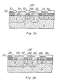
- Figure 1 illustrates, in cross-section, bipolar transistor 3, p-channel MOS transistor 5 and n-channel MOS transistor 7.
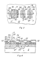
- Figure 3 is a plan view of transistors 3, 5, and 7 of Figure 1.
- the structure is formed into substrate 2 which, in this embodiment is p-type silicon.
- Buried n+ region 8 in bipolar transistor 3 serves as a sub-collector, in the conventional manner, with n+ region 52 providing a surface contact thereto.
- N region 20 in bipolar transistor 3 is the collector region thereof, and is disposed over buried n+ region 8.
- n region 20 is formed in an epitaxial layer grown over substrate 2 after the implantation of dopant for forming buried n+ region 8.
- Intrinsic base 69 is a p-type region disposed within n region 20 in bipolar transistor 3, and emitter region 80 is an n-type region disposed within intrinsic base region 69. Intrinsic base region 69 is isolated from diffused collector contact 52 by field oxide 32. Emitter region 80 is, in this embodiment, formed by the diffusion of n-type dopant from polysilicon emitter electrode 72e in the conventional manner. Extrinsic base region 82 is a p-type region which is more heavily doped than intrinsic base region 69. As is well known in the art, extrinsic base region 82 provides a relatively low series resistance contact from the surface of the structure to intrinsic base region 69.
- P-channel MOS transistor 5 is formed into n-type region 20, which is disposed over buried n+ region 8 in the same manner as for bipolar transistor 3.
- the use of similar n-type regions 20 both as the collector region for bipolar transistor 3 and for the n-well for p-channel MOS transistor 5 provides for efficiency in the manufacture of the structure.
- the provision of n+ region 8 under n-well 20 in MOS transistor 5 is useful to provide a constant bias throughout n-well 20, thereby reducing the tendency of the structure to enter a latchup condition.
- an n+ diffusion region 85 may be provided within n-well 20 to make contact to buried n+ region 8 from the surface, in a similar manner as collector contact 52, as described in said copending application S.N. 366,224. Such contact is useful in biasing the n-well 20 to the same potential as the source of the transistor.
- Gate electrode 72p is disposed over n-well 20, and is insulated therefrom by gate oxide 62.
- P-type source/drain regions 84 are disposed in self-aligned manner to gate electrode 72p (with sidewall oxide filaments 78 disposed along the sides thereof), in the conventional manner.
- p-type source/drain regions 84 may be formed by the same ion implantation (and subsequent diffusion) as used for the formation of extrinsic base region 82 in bipolar transistor 3.
- N-channel MOS transistor 7 is similarly constructed as p-channel MOS transistor 5, but of course with opposite conductivity type doped regions.
- Buried p region 12 is formed into substrate 2, in a manner similar to the formation of buried n+ regions 8 for bipolar transistor 3 and p-channel MOS transistor 5. While the buried p region 12 is optional for purposes of forming an operable circuit, as described in said copending application S.N. 366,224, the provision of buried p region 12 allows for reduced latchup sensitivity of the structure.
- P-well 24 is formed into the epitaxial layer over substrate 2 in a similar manner as n-type regions 20, and is lightly doped relative to buried p region 12. Referring to Figure 3, p-type well contact region 87 may be provided, if desired, to establish the potential of p-well 24 at that of the source of n-channel MOS transistor 7.
- n-channel MOS transistor 7 includes lightly-doped drain extensions to form a graded junction, for example as described in U.S. Patent No. 4,356,623 issued November 2, 1982, and U.S. Patent No. 4,566,175 issued January 28, 1986, both assigned to Texas Instruments Incorporated. It should of course be understood that n-channel MOS transistor 7 may alternatively be formed with abrupt junctions, if desired.
- emitter electrode 72e and gate electrodes 72n and 72p may be used as emitter electrode 72e and gate electrodes 72n and 72p, including, for example, amorphous silicon and deposited refractory metal silicides, such as molybdenum, tungsten, or titanium silicide.
- Transistors 3, 5 and 7 are isolated from one another by field oxide structures 32.
- the n-type regions 20 (and buried n+ regions 8) of bipolar transistor 3 and p-channel MOS transistor 5 are isolated from one another by buried p region 12′ underlying p region 24′, both of which are disposed under a field oxide structure 32. In this way, the n-type regions 20 of the two transistors may be at different potentials.
- junction isolation provided by a reversed biased p-n junction between buried n+ region 8 and buried p region 12, as well as between n-well 20 and p-well 24 where the junction underlies field oxide 32, is sufficient provided that proper bias is established in the wells relative to one another.
- alternative methods of isolation for example the trench isolation schemes described in U.S. Patent No. 4,631,803 issued December 30, 1986, and U.S. Patent No. 4,835,115 issued May 30, 1989, both assigned to Texas Instruments Incorporated, are equivalently applicable to this embodiment of the invention.
- the structure according to the instant invention includes a dielectric layer 70 underlying emitter electrode 72e.
- Dielectric layer 70 is substantially thicker than gate dielectric 62 underlying the gates 72p and 72n of MOS transistors 5 and 7.
- gate dielectric 62 may be made up of thermal silicon dioxide having a thickness on the order of 10 to 30 nm, while dielectric layer 70 may be on the order of 75 to 150 nm thick.
- Dielectric layer 70 is preferably a deposited dielectric such as silicon dioxide deposited by way of LPCVD.
- gate dielectric 62 is also present in bipolar transistor 3 over intrinsic base region 69, and underlying dielectric layer 70.
- Gate dielectric 62 in this location protects the silicon surface of intrinsic base region 69 from contamination which may be present in deposited dielectric layer 70, both during and after its deposition.
- sidewall oxide filaments 78 are provided on the sides of the gate electrodes 72p and 72n for the MOS transistors, and also on the side of the stack consisting of emitter electrode 72e and dielectric layer 70 for bipolar transistor 3.
- the preferred embodiment of the method for forming the structure of Figure 1 may result in a polysilicon filament 72f along the side of dielectric layer 70 overlying field oxide 32; a sidewall oxide filament 78 passivates this filament 72f so that its presence is harmless to the functionality and reliability of the structure of Figure 1.
- materials other than silicon dioxide may be used as sidewall filaments 78, such materials including silicon nitride and undoped polycrystalline silicon.
- the sidewall filaments be of a material other than silicon, especially if self-aligned silicidation of the surface regions (such as collector contact 52, extrinsic base 82, and source/drain regions 84 and 86) and the polysilicon structures 72e, 72p and 72n is to be performed, for example as described in U.S. Patent No. 4,384,301 issued May 17, 1983, and assigned to Texas Instruments Incorporated.
- dielectric layer 70 underlying emitter electrode 72e provides advantages in the resulting structure. Firstly, the thickness of dielectric layer 70 provides for reduced emitter-base capacitance, relative to what this parasitic capacitance would be if a thinner dielectric, such as on the order of gate dielectric 62, were used under emitter electrode 72e. This is, of course, due to the inversely proportional relationship of capacitance to dielectric thickness, making it preferable to have a thicker dielectric between the emitter electrode and the base region in order to reduce such capacitance.
- the thick dielectric layer 70 allows for contact to emitter electrode 72e to be made by metal or other material directly over the emitter region, for example at location 90 illustrated in Figure 3.
- a thinner dielectric such contact is generally prohibited as the etching of the contact directly over the emitter, as such a thin dielectric is inherently weaker to stress from subsequent processing steps such as contact etch, and metal deposition and sinter.
- the effect of such stress degrading the dielectric between the emitter and base is electrical leakage therebetween.
- Such leakage will especially be a problem in the event that the contact via is overetched through the emitter electrode, in which case the dielectric under the emitter electrode will be further thinned, in turn further increasing the emitter-to-base capacitance.
- the dielectric may be etched completely through, shorting the overlying metal and the emitter electrode to the base region. If a thin dielectric such as on the order of gate dielectric 62 is placed under emitter electrode 72e, the metal contact to emitter electrode 72e will need to be located away from the emitter region 80, for example at a location over field oxide 32 in order to avoid such problems. Such contacting of emitter electrode 72e thus requires that the size of the transistor 3 is increased, limiting the density of the integrated circuit. The provision of a relatively thick dielectric layer 70 under emitter electrode 72e allows for the contact to be placed directly over emitter region 80 without the problems described hereinabove.
- S.N. 366,224 describes a method where a thermally grown oxide which is thicker than the MOS gate dielectric is formed over the base region, directed toward solution of the above-noted problems. It has been found that a deposited dielectric layer 70 of the instant invention can provide further benefit over a thermal base oxide. For example, for a given rate of formation, silicon dioxide may be deposited at a lower temperature than that at which it can be thermally grown. Such reduced temperature allows for reduced diffusion (both in depth and laterally) of dopant in the structure at the time of the deposition. With the current trend toward shallower diffusion depths, and sub-micron lateral spacing, tighter control of the diffusion of dopant is much desired.
- the thickness of dielectric layer 70 can be optimized independently from such other variables as diffusion of dopant.
- LOC local oxidation
- a thermally grown oxide can form the well-known bird's beak and bird's head at the interface between the oxide and an oxidation mask (such as silicon nitride).
- LOC local oxidation
- Such artifacts of oxidation can be reduced by reducing the thickness of the oxide which is thermally grown.
- a deposited dielectric layer 70 can, however, be deposited to the desired thickness without concern for such artifacts, since no silicon is consumed during deposition which would cause stress at the corners of the masking layer.
- buried n+ regions 8 and buried p regions 12 (and 12′) are formed by masked ion implantation into substrate 2, after which an epitaxial layer is formed thereover. It is preferable that the epitaxial layer is relatively lightly-doped, as described in said application S.N.
- n-well 24 into which the n-channel MOS transistor 5 is to be formed does not have to substantially counterdope n-type material; such counterdoping has been found to adversely impact the carrier mobility in the channel of the transistor.
- a heavier doped epitaxial layer may be formed thereover, if a single well implant is desired (with the epitaxial layer serving as the well for the opposite conductivity type MOS transistors). Masked implants are then performed, followed by annealing, to form n-type regions 20 and p-type regicns 24 (and 24′). Ion implantation and annealing can be performed in order to form deep n+ collector contact region 52, as described in said application S.N. 366,224, if desired.
- Field oxide regions 32 are then formed by way of conventional field oxide formation techniques such as LOCOS.
- LOCOS Low-power MOS
- U.S. Patent No. 4,541,167 issued September 17, 1985, and assigned to Texas Instruments Incorporated describes a particularly beneficial method for forming LOCOS structures using a polysilicon buffer layer in the oxidation mask.
- Other isolation techniques such as the afore-mentioned trench isolation structures, or recessed isolation oxide methods, such as described in U.S. Patent No. 4,580,330 issued April 8, 1986 and assigned to Texas Instruments Incorporated, may alternatively be used for the formation of such isolation structures.
- conventional field oxide structures 32 are used in this embodiment of the invention.
- dummy gate oxide 34 Disposed over the moat regions of the surface of the structure in Figure 2a (moat regions defined as those portions of the surface at which field oxide 32 is not present, such regions to be the locations at which active devices are to be formed) is dummy gate oxide 34.
- dummy gate oxide 34 is provided so that ion implantation, such as may be desired for adjusting the threshold voltages of the MOS transistors, will not "channel” to an undesired and uncontrollable depth into the moat regions.
- Dummy gate oxide 34 is referred to as "dummy”, since it will be removed by way of a deglaze after the V t adjust implant and replaced with gate dielectric 62, as shown in Figure 2b.
- Gate dielectric 62 is formed of conventional material of conventional thicknesses for MOS transistors.
- gate dielectric may be formed of thermal silicon dioxide of a thickness in the range of 10 nm to 30 nm.
- Other conventional dielectric material such as deposited silicon nitride may be used as gate dielectric 62, or further in the alternative may be formed of a stack of dielectric material, such as a stacked layer of oxide/nitride/oxide.
- a layer of polycrystalline silicon 68 is deposited by way of CVD over the surface of the structure. This layer may be doped in-situ during deposition, or as will be described hereinbelow, may be doped by way of a blanket or masked ion implantation.
- Polysilicon layer 68 in this embodiment is of a thickness on the order of 100 to 200 nm, resulting in the structure of Figure 2c.
- Masking layer 66 for example a layer of photoresist, is placed over the structure, and photolithographically patterned and developed to expose the portion of the structure at which the base of bipolar transistor 3 is to be formed (i.e., including both intrinsic base 69 and extrinsic base 82 of Figure 1). The moat regions at which both types of MOS transistors 5 and 7 are to be formed are protected by masking layer 66, as is the collector contact region 52, as shown in Figure 2d. With masking layer 66 in place, polysilicon layer 68 is etched from the location at which intrinsic base 69 and extrinsic base 82 will be located. Conventional wet or dry polysilicon etches may be used; a preferred example of a dry polysilicon etch is described in U.S. Patent No. 4,502,915 issued March 5, 1985, and assigned to Texas Instruments Incorporated.
- Ion implantation of boron is then performed in order to dope the portion of n region 20 with the intrinsic base implant, as shown in Figure 2d.
- the intrinsic base implant is performed after polysilicon layer 68 has been etched from the moat region in bipolar transistor 3, through gate dielectric 62 only.
- the intrinsic base implant also can be performed prior to the etch of polysilicon layer 68 in the bipolar region, through both gate dielectric 62 and polysilicon layer 68.
- the implant dose and energy can be determined by one of ordinary skill in the art to arrive at the desired impurity concentration in the base of the desired bipolar transistor 3.
- a base implant of boron of a dose of 7.0E13 cm ⁇ 2 at an energy of 10 keV is performed, where the n-well impurity concentration is on the order of 4E16 cm ⁇ 3 at the surface.
- an example of an intrinsic base implant would be a boron implant of a dose of 5.8E13 at an energy of 40 keV.
- Dielectric layer 70 may be any conventional dielectric material, but preferably is silicon dioxide which is deposited by way of decomposition of tetraethyl orthosilicate (TEOS), preferably under LPCVD conditions, in the conventional manner.
- TEOS tetraethyl orthosilicate
- dielectric layer 70 is to be deposited to the thickness desired for such a structure in order to minimize parasitic emitter-base capacitance and provide the necessary film integrity to place a metal contact to emitter electrode 72e directly thereover, if desired.
- the thickness of dielectric layer 70 is is on the order of 50 to 150
- the thickness of dielectric layer 70 can be controlled independently relative to other process variables, such as depth of intrinsic base 69.
- depth of intrinsic base 69 an important parameter in the performance of a bipolar transistor is the base width.
- the base width is determined by the depth of the intrinsic base. It is therefore important that the diffusion of the implanted dopant 69 of Figure 2f (which will result in intrinsic base region 69) be well controlled in order to optimize the base width of the transistor 3, and its performance.
- a deposited dielectric layer 70 as described above can be done at temperatures which are relatively low relative to those of thermal oxidation; for example, LPCVD of silicon dioxide by TEOS decomposition can be done at temperatures in the range of 650 to 750 degrees Celsius. Such low temperatures will diffuse the implanted boron 69 only minimally, allowing control of the depth of the intrinsic base region with a single anneal step later in the process. Since diffusion of the implanted base dopant is minimal during LPCVD of dielectric layer 70, the thickness of dielectric layer 70 can be optimized for film strength and for reduction of the parasitic capacitance, without limiting the film thickness due to thermal considerations.
- the intrinsic base implant is performed after formation of gate dielectric 62, whether before or after the etch of polysilicon layer 68. This further reduces uncontrolled diffusion of the implanted base dopant, as the dopant is not present during the thermal oxidation process conventionally used to form gate dielectric 62. Furthermore, in either of the above alternatives, the intrinsic base implant is performed through relatively thin gate dielectric 62, which is generally well-controlled since it is generally thermally grown oxide.
- the method of the invention provides still further control of the base width relative to prior methods which implant the intrinsic base through a thicker oxide on the order of 140 nm, since variations in such thicker oxide layers have a more significant impact on the profile of the dopant implanted therethrough.
- FIG. 2g another masking layer 73 of photoresist is illustrated as present over dielectric layer 70.
- Masking layer 73 is lithographically exposed and subsequently developed so that it protects dielectric layer 70 at locations at which the eventual emitter electrode 72e is to overlap intrinsic base region 69. It should be noted that opening 71 is defined, at which the emitter region will be formed. A portion of dielectric layer 70 is also protected at location 74 over intrinsic base region 69 where extrinsic base region 82 will eventually be formed, so that the polysilicon etch used in the formation of the gate and emitter electrodes 72 will not etch into the single crystal silicon thereat.
- Figure 2h illustrates the structure after an oxide etch is performed to remove dielectric layer 70 from the locations not protected by masking layer 72, and after removal of masking layer 72. It is preferable to use an etch which selectively etches silicon dioxide relative to silicon so that the remaining portions of polysilicon layer 68 and of n-type region 20 are not substantially etched by the removal of dielectric layer 70.
- a conventional example of such an etch is a plasma etch, using CHF3, C2F6 and He as active species.
- both dielectric layer 70 and gate dielectric 62 are removed at location 71, at which the emitter region will be formed.
- Polysilicon layer 72 is then formed overall to a thickness on the order of 100 to 300 nm, preferably by way of LPCVD, to result in the structure illustrated in Figure 2i.
- the two polysilicon layers 68 and 72 will effectively merge into a single layer (hereinafter referred to as layer 72).
- layer 72 At the location 71 of the emitter contact, polysilicon layer 72 will be in contact with n region 20.
- a blanket n-type implant is performed, to provide dopant thereinto which can diffuse to form emitter region 80 in bipolar transistor 3, and which will increase the conductivity of the gate electrodes 72 in MOS transistors 5 and 7.
- An example of a preferred method of implanting polysilicon layer 72, wherein a shallow emitter junction is provided while yet providing highly conductive polysilicon emitter electrode, is described in copending application S.N. 306,439 filed February 3, 1989, and assigned to Texas Instruments Incorporated.
- n-type implant method results in all polysilicon structures 72 being heavily n-type doped. It should be noted that if it is desired that some portions of polysilicon layer 72 not be doped n-type, for example if gate electrode 72p for p-channel MOS transistor 5 is to be doped p-type, a masking layer may be provided and the implant of Figure 2i can be done with portions of layer 72 masked therefrom.
- a masking layer (not shown) is then formed over the structure to define the geometries of the gate electrodes of MOS transistors 5 and 7, and of the emitter electrode for bipolar transistor 3.
- a polysilicon etch is then performed, in a similar manner as described above for the etching of polysilicon layer 68.
- the resulting structure is shown in Figure 2j, where emitter electrode 72e, and gate electrodes 72p and 72n are formed in the desired locations.
- a filament of polysilicon layer 68 such filament referred to as filament 72f in Figure 2j, may remain after the polysilicon etch, especially if the etch used is substantially anisotropic.
- filament 72f may be passivated so as to be electrically harmless, as will be described hereinbelow.
- a brief isotropic polysilicon etch for example a conventional wet polysilicon etch, may be done in order to remove filament 72f, if desired.
- sidewall filaments 78 are preferably formed by deposition of silicon dioxide followed by an anisotropic oxide etch.
- the anisotropic oxide etch used to form sidewall filaments 78 will also remove dielectric layer 70 and gate dielectric 62 from location 74 in the bipolar moat region. The surface of the intrinsic base region 69 at location 74 will thus be exposed after this etch, so that extrinsic base region 82 can be formed thereat, via ion implantation and diffusion.
- Ion implantation for formation of the n-type source/drain regions 86 and for formation of the p-type source/drain regions 84 and extrinsic base region 82, can be formed in the conventional manner, followed by a high temperature anneal in order to diffuse the dopant implanted into the single-crystal silicon, as well as the dopant implanted into emitter electrode 72e, to the desired depths.
- the resultant transistor is illustrated in Figures 1 and 3, such construction described hereinabove relative to these figures.
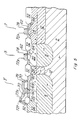
- emitter electrode 72e After removal of dielectric layer 70 in all locations except over the intrinsic base region 69, at the point in the process illustrated by Figure 2h, it may be desirable to narrow the size of emitter opening 71 through dielectric layer 70. This is especially true where the size of eventual emitter region 80 is to be smaller than that which may be formed by conventional lithography and etch processes, especially with a relatively thick (100 nm) dielectric layer 70 to be etched through in forming emitter opening 70. In order to form such a smaller emitter opening (and extrinsic base region 82), sidewall dielectric filaments 90 can be formed on the sides of remaining dielectric layer 70 in bipolar transistor 3.
- filaments 90 is performed in the conventional sidewall filament manner, i.e., by the deposition of a material such as silicon dioxide followed by anisotropic etching thereof.
- Figure 4 illustrates the formation of filaments 90 on the structure at this point in the fabrication process. The width of emitter opening 71′ can thus be reduced from that which could be made by conventional lithographic processing.
- the fabrication method according to this alternative embodiment will be completed in the same manner as described above.
- the resultant transistor 3′ illustrated in cross-section in Figure 5, will have a smaller emitter region 80 and extrinsic base region 82, as compared to that of transistor 3 of Figure 1. Accordingly, this alternative embodiment is especially applicable when the structure of Figure 1 is to be scaled downward in size. The ability to perform such scaling is widely desired in the semiconductor processing art.
- interconnecting metallization is then formed for making contact to the active regions of Figures 1 and 5, in the conventional manner, and as described in said copending application S.N. 366,224.
- Individual circuits are then separated from portions of substrate 20, and external connections made thereto by way of wire bonding, direct bump connection, or the like, as is well known in the art.
- the individual circuits may then be packaged into a dual-in-line package, a chip carrier, or another type of package.
- An example of such a package is described in U.S. Patent No. 4,495,376 issued January 22, 1985 and assigned to Texas Instruments Incorporated.
Landscapes
- Bipolar Transistors (AREA)
- Metal-Oxide And Bipolar Metal-Oxide Semiconductor Integrated Circuits (AREA)
Applications Claiming Priority (2)
| Application Number | Priority Date | Filing Date | Title |
|---|---|---|---|
| US38396089A | 1989-07-21 | 1989-07-21 | |
| US383960 | 1989-07-21 |
Publications (2)
| Publication Number | Publication Date |
|---|---|
| EP0409041A1 true EP0409041A1 (fr) | 1991-01-23 |
| EP0409041B1 EP0409041B1 (fr) | 1995-10-11 |
Family
ID=23515479
Family Applications (1)
| Application Number | Title | Priority Date | Filing Date |
|---|---|---|---|
| EP90113112A Expired - Lifetime EP0409041B1 (fr) | 1989-07-21 | 1990-07-10 | Méthode pour la formation d'un oxyde de base épais dans un procédé BICMOS |
Country Status (4)
| Country | Link |
|---|---|
| EP (1) | EP0409041B1 (fr) |
| JP (1) | JP3247106B2 (fr) |
| DE (1) | DE69022906T2 (fr) |
| TW (1) | TW199938B (fr) |
Cited By (2)
| Publication number | Priority date | Publication date | Assignee | Title |
|---|---|---|---|---|
| GB2257296A (en) * | 1991-06-27 | 1993-01-06 | Samsung Electronics Co Ltd | Bicmos device and manufacturing method therfor |
| EP1128422A1 (fr) * | 2000-02-22 | 2001-08-29 | Infineon Technologies AG | Procédé de fabrication de transistors bipolaires dans un procédé pour BiCMOS |
Citations (3)
| Publication number | Priority date | Publication date | Assignee | Title |
|---|---|---|---|---|
| EP0283135A1 (fr) * | 1987-02-20 | 1988-09-21 | Fairchild Semiconductor Corporation | Procédé de fabrication d'une structure semi-conductrice |
| EP0320217A2 (fr) * | 1987-12-07 | 1989-06-14 | Texas Instruments Incorporated | Procédé pour fabriquer un transistor du type twin-well-BICMOS |
| EP0320271A2 (fr) * | 1987-12-08 | 1989-06-14 | Rhoderton Corporation N.V. | Diméthylsulfoxyde et analogues comme agents antirétroviraux |
-
1990
- 1990-07-10 EP EP90113112A patent/EP0409041B1/fr not_active Expired - Lifetime
- 1990-07-10 DE DE69022906T patent/DE69022906T2/de not_active Expired - Fee Related
- 1990-07-20 JP JP19093290A patent/JP3247106B2/ja not_active Expired - Fee Related
-
1991
- 1991-01-04 TW TW080100079A patent/TW199938B/zh active
Patent Citations (3)
| Publication number | Priority date | Publication date | Assignee | Title |
|---|---|---|---|---|
| EP0283135A1 (fr) * | 1987-02-20 | 1988-09-21 | Fairchild Semiconductor Corporation | Procédé de fabrication d'une structure semi-conductrice |
| EP0320217A2 (fr) * | 1987-12-07 | 1989-06-14 | Texas Instruments Incorporated | Procédé pour fabriquer un transistor du type twin-well-BICMOS |
| EP0320271A2 (fr) * | 1987-12-08 | 1989-06-14 | Rhoderton Corporation N.V. | Diméthylsulfoxyde et analogues comme agents antirétroviraux |
Non-Patent Citations (1)
| Title |
|---|
| PATENT ABSTRACTS OF JAPAN * |
Cited By (2)
| Publication number | Priority date | Publication date | Assignee | Title |
|---|---|---|---|---|
| GB2257296A (en) * | 1991-06-27 | 1993-01-06 | Samsung Electronics Co Ltd | Bicmos device and manufacturing method therfor |
| EP1128422A1 (fr) * | 2000-02-22 | 2001-08-29 | Infineon Technologies AG | Procédé de fabrication de transistors bipolaires dans un procédé pour BiCMOS |
Also Published As
| Publication number | Publication date |
|---|---|
| JPH03148862A (ja) | 1991-06-25 |
| EP0409041B1 (fr) | 1995-10-11 |
| JP3247106B2 (ja) | 2002-01-15 |
| TW199938B (fr) | 1993-02-11 |
| DE69022906D1 (de) | 1995-11-16 |
| DE69022906T2 (de) | 1996-03-21 |
Similar Documents
| Publication | Publication Date | Title |
|---|---|---|
| US5171702A (en) | Method for forming a thick base oxide in a BiCMOS process | |
| US4958213A (en) | Method for forming a transistor base region under thick oxide | |
| US4819052A (en) | Merged bipolar/CMOS technology using electrically active trench | |
| US5455189A (en) | Method of forming BICMOS structures | |
| US5374845A (en) | Process for reduced emitter-base capacitance in bipolar transistor | |
| US4962053A (en) | Bipolar transistor fabrication utilizing CMOS techniques | |
| JP2003338558A (ja) | 半導体装置及び半導体装置の製造方法 | |
| EP0381071A2 (fr) | Méthode modifiée de formation des émetteurs dans un procédé BI-CMOS | |
| US5389553A (en) | Methods for fabrication of transistors | |
| US20030080394A1 (en) | Control of dopant diffusion from polysilicon emitters in bipolar integrated circuits | |
| EP0278619A1 (fr) | Procédé pour fabriquer des structures intégrées comportant des transistors bipolaires et de type CMOS | |
| EP0233202B1 (fr) | Fabrication d'un dispositif a semi-conducteur avec de l'oxyde enfoui | |
| EP0281235B1 (fr) | Procédé pour fabriquer un transistor bipolaire utilisant des technologies de type CMOS | |
| EP0399231A2 (fr) | Dispositif à semi-conducteur et procédé pour sa fabrication | |
| EP0320217B1 (fr) | Procédé pour fabriquer un transistor du type twin-well-BICMOS | |
| US5422290A (en) | Method of fabricating BiCMOS structures | |
| WO2002080281A1 (fr) | Transistor bipolaire a courant horizontal | |
| EP0656660B1 (fr) | Procédé pour fabriquer des BiCMOS | |
| US6251744B1 (en) | Implant method to improve characteristics of high voltage isolation and high voltage breakdown | |
| US5013671A (en) | Process for reduced emitter-base capacitance in bipolar transistor | |
| US5065209A (en) | Bipolar transistor fabrication utilizing CMOS techniques | |
| EP0409041B1 (fr) | Méthode pour la formation d'un oxyde de base épais dans un procédé BICMOS | |
| US6790736B2 (en) | Method for manufacturing and structure of semiconductor device with polysilicon definition structure | |
| WO2005117104A1 (fr) | Dispositif a semi-conducteur et procede de production dudit dispositif | |
| US5451530A (en) | Method for forming integrated circuits having buried doped regions |
Legal Events
| Date | Code | Title | Description |
|---|---|---|---|
| PUAI | Public reference made under article 153(3) epc to a published international application that has entered the european phase |
Free format text: ORIGINAL CODE: 0009012 |
|
| AK | Designated contracting states |
Kind code of ref document: A1 Designated state(s): DE FR GB IT NL |
|
| 17P | Request for examination filed |
Effective date: 19910730 |
|
| 17Q | First examination report despatched |
Effective date: 19931129 |
|
| GRAA | (expected) grant |
Free format text: ORIGINAL CODE: 0009210 |
|
| AK | Designated contracting states |
Kind code of ref document: B1 Designated state(s): DE FR GB IT NL |
|
| REF | Corresponds to: |
Ref document number: 69022906 Country of ref document: DE Date of ref document: 19951116 |
|
| ITF | It: translation for a ep patent filed | ||
| ET | Fr: translation filed | ||
| PLBE | No opposition filed within time limit |
Free format text: ORIGINAL CODE: 0009261 |
|
| STAA | Information on the status of an ep patent application or granted ep patent |
Free format text: STATUS: NO OPPOSITION FILED WITHIN TIME LIMIT |
|
| 26N | No opposition filed | ||
| REG | Reference to a national code |
Ref country code: GB Ref legal event code: IF02 |
|
| PGFP | Annual fee paid to national office [announced via postgrant information from national office to epo] |
Ref country code: DE Payment date: 20070731 Year of fee payment: 18 |
|
| PGFP | Annual fee paid to national office [announced via postgrant information from national office to epo] |
Ref country code: GB Payment date: 20070618 Year of fee payment: 18 |
|
| PGFP | Annual fee paid to national office [announced via postgrant information from national office to epo] |
Ref country code: NL Payment date: 20070619 Year of fee payment: 18 Ref country code: IT Payment date: 20070714 Year of fee payment: 18 |
|
| PGFP | Annual fee paid to national office [announced via postgrant information from national office to epo] |
Ref country code: FR Payment date: 20070706 Year of fee payment: 18 |
|
| GBPC | Gb: european patent ceased through non-payment of renewal fee |
Effective date: 20080710 |
|
| NLV4 | Nl: lapsed or anulled due to non-payment of the annual fee |
Effective date: 20090201 |
|
| PG25 | Lapsed in a contracting state [announced via postgrant information from national office to epo] |
Ref country code: DE Free format text: LAPSE BECAUSE OF NON-PAYMENT OF DUE FEES Effective date: 20090203 |
|
| REG | Reference to a national code |
Ref country code: FR Ref legal event code: ST Effective date: 20090331 |
|
| PG25 | Lapsed in a contracting state [announced via postgrant information from national office to epo] |
Ref country code: NL Free format text: LAPSE BECAUSE OF NON-PAYMENT OF DUE FEES Effective date: 20090201 |
|
| PG25 | Lapsed in a contracting state [announced via postgrant information from national office to epo] |
Ref country code: GB Free format text: LAPSE BECAUSE OF NON-PAYMENT OF DUE FEES Effective date: 20080710 |
|
| PG25 | Lapsed in a contracting state [announced via postgrant information from national office to epo] |
Ref country code: IT Free format text: LAPSE BECAUSE OF NON-PAYMENT OF DUE FEES Effective date: 20080710 Ref country code: FR Free format text: LAPSE BECAUSE OF NON-PAYMENT OF DUE FEES Effective date: 20080731 |