EP1128422A1 - Procédé de fabrication de transistors bipolaires dans un procédé pour BiCMOS - Google Patents
Procédé de fabrication de transistors bipolaires dans un procédé pour BiCMOS Download PDFInfo
- Publication number
- EP1128422A1 EP1128422A1 EP00103726A EP00103726A EP1128422A1 EP 1128422 A1 EP1128422 A1 EP 1128422A1 EP 00103726 A EP00103726 A EP 00103726A EP 00103726 A EP00103726 A EP 00103726A EP 1128422 A1 EP1128422 A1 EP 1128422A1
- Authority
- EP
- European Patent Office
- Prior art keywords
- layer
- base
- placeholder
- emitter
- emitter contact
- Prior art date
- Legal status (The legal status is an assumption and is not a legal conclusion. Google has not performed a legal analysis and makes no representation as to the accuracy of the status listed.)
- Withdrawn
Links
Images




Classifications
-
- H—ELECTRICITY
- H10—SEMICONDUCTOR DEVICES; ELECTRIC SOLID-STATE DEVICES NOT OTHERWISE PROVIDED FOR
- H10D—INORGANIC ELECTRIC SEMICONDUCTOR DEVICES
- H10D10/00—Bipolar junction transistors [BJT]
- H10D10/01—Manufacture or treatment
- H10D10/051—Manufacture or treatment of vertical BJTs
-
- H—ELECTRICITY
- H10—SEMICONDUCTOR DEVICES; ELECTRIC SOLID-STATE DEVICES NOT OTHERWISE PROVIDED FOR
- H10D—INORGANIC ELECTRIC SEMICONDUCTOR DEVICES
- H10D84/00—Integrated devices formed in or on semiconductor substrates that comprise only semiconducting layers, e.g. on Si wafers or on GaAs-on-Si wafers
- H10D84/01—Manufacture or treatment
- H10D84/0107—Integrating at least one component covered by H10D12/00 or H10D30/00 with at least one component covered by H10D8/00, H10D10/00 or H10D18/00, e.g. integrating IGFETs with BJTs
- H10D84/0109—Integrating at least one component covered by H10D12/00 or H10D30/00 with at least one component covered by H10D8/00, H10D10/00 or H10D18/00, e.g. integrating IGFETs with BJTs the at least one component covered by H10D12/00 or H10D30/00 being a MOS device
-
- H—ELECTRICITY
- H10—SEMICONDUCTOR DEVICES; ELECTRIC SOLID-STATE DEVICES NOT OTHERWISE PROVIDED FOR
- H10D—INORGANIC ELECTRIC SEMICONDUCTOR DEVICES
- H10D84/00—Integrated devices formed in or on semiconductor substrates that comprise only semiconducting layers, e.g. on Si wafers or on GaAs-on-Si wafers
- H10D84/01—Manufacture or treatment
- H10D84/02—Manufacture or treatment characterised by using material-based technologies
- H10D84/03—Manufacture or treatment characterised by using material-based technologies using Group IV technology, e.g. silicon technology or silicon-carbide [SiC] technology
- H10D84/038—Manufacture or treatment characterised by using material-based technologies using Group IV technology, e.g. silicon technology or silicon-carbide [SiC] technology using silicon technology, e.g. SiGe
Definitions
- the invention relates to a method for producing a bipolar transistor in a BICMOS process.
- the substrate is in the emitter contact area first deposited a thin oxide layer. Then a layer on the thin oxide layer made of polysilicon and an overlying layer of one Nitride applied. The last two layers are outside of the emitter contact area down to the thin oxide layer etched back, so that only in the emitter contact area Layer of polysilicon and the layer above remains with a nitride.
- Around the emitter contact area to form an enclosing base contact layer becomes the substrate around the emitter contact area by the bombardment doped with ions.
- a next step of the process to grow the thin oxidation layer so that overall results in a thicker oxidation layer than before.
- an outer bead-like thickening of the oxide layer which follows is called a spacer.
- a spacer After oxidizing the thin oxide layer is in the emitter contact area the nitride layer on top and the one underneath, polysilicon still present in a central area removed. This will expose the spacers and it will result there is an oxide layer in the emitter contact area has a pot-like profile. This is followed in the emitter contact area the implantation through the oxide layer the base layer in the substrate. Finally, in the emitter contact area an emitter layer of polysilicon is deposited. This is followed by the formation of lateral spacers and the contacting of the emitter layer and the base contact layer.
- a disadvantage of the known method is that the width of the Emitters by the inner diameter of the edge of the emitter contact zone circumferential spacer depends. Because the spacer is generated in an oxidation process, which in its process is difficult to control. Also done the implantation of the base through the oxide layer, which results in a different doping of the base layer has, especially in the outer under the spacer located areas of the base layer. Because of the weak Doping of the outer base layer results in a high outer layer Base resistance between the edge of the emitter and the Beginning of the base contact layer. The outer baseband resistance is also due to the uncertainties mentioned in the manufacture of the spacer from the thin Vary the oxide layer. Both effects are for the high frequency behavior of the bipolar transistor disadvantageous.
- the invention is based on this prior art based on the task of being able to be integrated into a BICMOS process Manufacturing process for bipolar transistors with low to specify the external baseline resistance.
- the placeholder is used on the one hand, the substrate during the implantation of the base contact layer to cover and thereby the expansion of the To determine the base contact layer to the emitter contact area.
- the dimensions of the placeholder also determine the other the expansion of the emitter contact hole and thus the expansion that through the emitter contact hole in the substrate implanted base layer.
- the width of the emitter is finally in the inventive Move through the spacers in the emitter contact hole certainly. This makes the width of the emitter essential defined more precisely than in the prior art.
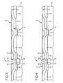
- Figures 1 to 4 illustrate a BICMOS process integrable manufacturing process for a bipolar Transistor.
- the associated collector contact area is in Figures 1 to 4 not shown.
- the transistor also only partially includes itself Shown field effect transistor 2 with a gate 3 and Drain 4 on.
- the layer structure 5 first the insulating areas 6 are made of field oxide. After that a layer is deposited and structured made of polysilicon, which, among other things, the gate 3 of the field effect transistor 2 forms. Through implantation is then Substrate 5 a lightly doped region 8 of the drain 4 is formed.
- a placeholder 9 in the emitter contact area for example made from a nitride.
- the placeholder 9 serves in one subsequent implantation process as a mask to a in Substrate 5 implanted highly doped base contact layer 10 to limit inward expansion.
- a drain contact layer 11 in the Area of the field effect transistor 2 implanted is also also a drain contact layer 11 in the Area of the field effect transistor 2 implanted.
- insulating layers 12 which, for example, made of tetra ethyl orthosilicate become.
- the insulating layers then by chemical mechanical polishing leveled.
- the placeholder 9 is thereby exposed.
- the part lying on the insulating area 6 of the the layer forming the gate 3 is partially exposed.
- the placeholder 9 is etched out, so that an emitter contact hole 13 is formed.
- the implantation is also carried out first a pedestal collector 14.
- a pedestal collector 14 is often called SIC (Selectively Implanted Collector) designated.
- Base layer 15 implanted. Since the placeholder 9 on the one hand the lateral expansion of the base contact layer 10 inwards limited and on the other hand the lateral extent of the Determined emitter contact hole, arises from the implantation the base layer 15 a complementary to the base contact layer 10 Base layer 15. As a result, the base layer closes 15 directly to the highly doped base contact layer 10 on.
- the implantation process is followed by the production of spacers 16 in the emitter contact hole 13.
- the next process step, shown in FIG the emitter layer 17 is deposited in the emitter contact hole 13.
- the width of the emitter layer adjacent to the base layer 15 17 is determined by the distance between the spacers 16.
- the accuracy in the manufacture of the spacers 16 thus also determines the fluctuation range of the outer base track resistance between the edge of the emitter layer 17 and the base contact layer 10.
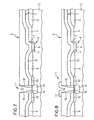
- FIG. 5 Exemplary embodiment is the connection to conductor tracks on others Way has been made.
- the insulating layer 12 made of tetra ethyl orthosilicate a further insulating layer 18 made of boron-containing phosphor glass (BPSG) applied.
- BPSG boron-containing phosphor glass
- the latter layer for example leveled by chemical mechanical polishing so that the placeholder 9 is exposed.
- the remaining process steps are the same as in the case of FIGS. 1 to 4 illustrated embodiment performed.
- the difference to the embodiment shown in Figures 1 to 4 allows the insulating layer 18 made of boron Phosphor glass, however, the direct application of a conductor track 19 on the emitter layer 17.
- FIGS. 5 to 9 permits thus to produce a particularly flat layer structure. It however requires precise adjustment of the ion beam at the implantation of the pedestal collector 14 and the base layer 15 to prevent unwanted shadowing of the ion beam.
- FIGS. 10 to 14 Another modified method is shown in FIGS. 10 to 14 shown.
- the method according to FIGS. 1 to 9 is the placeholder here 9 formed by the same layer that also the gate 3 of Field effect transistor 2 forms.
- the placeholder exists 9 not as in the exemplary embodiments from the figures 1 to 9 from a nitride, but from polysilicon.
- spacers 7 attached to the placeholder 9 outside. Since the insulating layers 12 are only removed to the extent until the one lying in the isolation area 6 on the field oxide Part of the gate layer 3 is exposed, it is necessary expose the placeholder 9 in an additional step, so that it can be removed.
- FIGS. 10 to 14 The method presented in FIGS. 10 to 14 is so far cheap than for the training of the placeholder 9 no additional process step is required. For that, however an additional etching step to etch the access opening 22 are accepted. In addition, the implantation the base contact layer 10 through the spacers 7 am Placeholder 9 hindered.
- the exemplary embodiments described with reference to FIGS. 1 to 14 has in common that the insulating layers 12 over the entire surface be applied and then removed as far until the placeholder is exposed.
- an insulating layer from a Oxide is selectively applied to a substrate.
- SELOX process Tetra-ethyl-ortho-silicate activated by ozone on monocrystalline Silicon is applied.
- the placeholder 9 is formed in the emitter contact area.
- it is a placeholder a nitride applied to the silicon substrate 5 is.
- the base contact layer 10 is then implanted, the placeholder 9 is used as a mask.
- a further process step then becomes the room Selective above the base contact layer 10 in the SELOX process filled with an insulating layer 23.
- the thickness of the insulation layer 23 corresponds to the thickness of the placeholder 9.
- the placeholder 9 is etched out and the pedestal collector 14 and the base layer 15 implanted. After that is done the manufacture of the spacers 16 and the subsequent one Deposition of the emitter layer 17.
- This method has the advantage that the insulating layer is not flattened 23 is required to expose the placeholder 9.
- the Placeholder 9 is part of the gate layer 3.
- Placeholder 9 is formed together with the gate of the field effect transistor 2 and, like this, is laterally limited by spacers 7. Since the process management for training the placeholder 9 is the same as that for forming the gate of the field effect transistor, comprises the base contact layer 10 in each case a lightly doped region 24 and a highly doped one Area 25.
- the lightly doped area of the base contact layer 24 corresponds to the lightly doped region 8 of the field effect transistor 2 and the highly doped region of Base contact layer 25 corresponds to drain contact layer 11 of the field effect transistor 2.
- the space above the base contact layer 10 is then im SELOX process selectively filled with the insulating layer 23.
- the height of the insulating layer 23 corresponds essentially the height of the placeholder 9.
- the Placeholder 9 etched out and the base layer 15 and the pedestal collector 14 implanted. Finally the separation takes place the emitter layer 17.
Landscapes
- Bipolar Transistors (AREA)
Priority Applications (1)
| Application Number | Priority Date | Filing Date | Title |
|---|---|---|---|
| EP00103726A EP1128422A1 (fr) | 2000-02-22 | 2000-02-22 | Procédé de fabrication de transistors bipolaires dans un procédé pour BiCMOS |
Applications Claiming Priority (1)
| Application Number | Priority Date | Filing Date | Title |
|---|---|---|---|
| EP00103726A EP1128422A1 (fr) | 2000-02-22 | 2000-02-22 | Procédé de fabrication de transistors bipolaires dans un procédé pour BiCMOS |
Publications (1)
| Publication Number | Publication Date |
|---|---|
| EP1128422A1 true EP1128422A1 (fr) | 2001-08-29 |
Family
ID=8167933
Family Applications (1)
| Application Number | Title | Priority Date | Filing Date |
|---|---|---|---|
| EP00103726A Withdrawn EP1128422A1 (fr) | 2000-02-22 | 2000-02-22 | Procédé de fabrication de transistors bipolaires dans un procédé pour BiCMOS |
Country Status (1)
| Country | Link |
|---|---|
| EP (1) | EP1128422A1 (fr) |
Cited By (3)
| Publication number | Priority date | Publication date | Assignee | Title |
|---|---|---|---|---|
| DE10358046A1 (de) * | 2003-12-05 | 2005-07-07 | IHP GmbH - Innovations for High Performance Microelectronics/Institut für innovative Mikroelektronik | Bipolartransistor mit erhöhtem Basisanschlussgebiet und Verfahren zu seiner Herstellung |
| RU2329567C1 (ru) * | 2006-11-16 | 2008-07-20 | Общество с ограниченной ответственностью ООО "Юник Ай Сиз" | Метод изготовления самосовмещенной бикмоп структуры субмикронных размеров |
| RU2368036C1 (ru) * | 2008-01-10 | 2009-09-20 | Михаил Иванович Лукасевич | Безэпитаксиальная структура биполярного транзистора |
Citations (6)
| Publication number | Priority date | Publication date | Assignee | Title |
|---|---|---|---|---|
| US4698127A (en) * | 1985-04-10 | 1987-10-06 | Fujitsu Limited | Process for fabricating a self-aligned bipolar transistor |
| EP0326211A1 (fr) * | 1988-01-25 | 1989-08-02 | Koninklijke Philips Electronics N.V. | Dispositif semi-conducteur et procédé de fabrication de ce dispositif |
| EP0409041A1 (fr) * | 1989-07-21 | 1991-01-23 | Texas Instruments Incorporated | Méthode pour la formation d'un oxyde de base épais dans un procédé BICMOS |
| US5147810A (en) * | 1990-01-09 | 1992-09-15 | Oki Electric Industry Co., Ltd. | Process for producing semiconductor device |
| US5516708A (en) * | 1994-11-17 | 1996-05-14 | Northern Telecom Limited | Method of making single polysilicon self-aligned bipolar transistor having reduced emitter-base junction |
| US5648279A (en) * | 1994-06-21 | 1997-07-15 | Nec Corporation | Method of manufacturing bipolar transistor having emitter region and external base region formed in self alignment manner |
-
2000
- 2000-02-22 EP EP00103726A patent/EP1128422A1/fr not_active Withdrawn
Patent Citations (6)
| Publication number | Priority date | Publication date | Assignee | Title |
|---|---|---|---|---|
| US4698127A (en) * | 1985-04-10 | 1987-10-06 | Fujitsu Limited | Process for fabricating a self-aligned bipolar transistor |
| EP0326211A1 (fr) * | 1988-01-25 | 1989-08-02 | Koninklijke Philips Electronics N.V. | Dispositif semi-conducteur et procédé de fabrication de ce dispositif |
| EP0409041A1 (fr) * | 1989-07-21 | 1991-01-23 | Texas Instruments Incorporated | Méthode pour la formation d'un oxyde de base épais dans un procédé BICMOS |
| US5147810A (en) * | 1990-01-09 | 1992-09-15 | Oki Electric Industry Co., Ltd. | Process for producing semiconductor device |
| US5648279A (en) * | 1994-06-21 | 1997-07-15 | Nec Corporation | Method of manufacturing bipolar transistor having emitter region and external base region formed in self alignment manner |
| US5516708A (en) * | 1994-11-17 | 1996-05-14 | Northern Telecom Limited | Method of making single polysilicon self-aligned bipolar transistor having reduced emitter-base junction |
Non-Patent Citations (1)
| Title |
|---|
| REUSS R H ET AL: "HIGH-PERFORMANCE SELF-ALIGNED NPN FOR BICMOS", MOTOROLA TECHNICAL DEVELOPMENTS,US,MOTOROLA INC. SCHAUMBURG, ILLINOIS, vol. 16, 1 August 1992 (1992-08-01), pages 100 - 103, XP000310374 * |
Cited By (5)
| Publication number | Priority date | Publication date | Assignee | Title |
|---|---|---|---|---|
| DE10358046A1 (de) * | 2003-12-05 | 2005-07-07 | IHP GmbH - Innovations for High Performance Microelectronics/Institut für innovative Mikroelektronik | Bipolartransistor mit erhöhtem Basisanschlussgebiet und Verfahren zu seiner Herstellung |
| DE10358046B4 (de) * | 2003-12-05 | 2010-06-17 | Ihp Gmbh - Innovations For High Performance Microelectronics / Leibniz-Institut Für Innovative Mikroelektronik | Bipolartransistor mit erhöhtem Basisanschlussgebiet und Verfahren zu seiner Herstellung |
| US7777255B2 (en) | 2003-12-05 | 2010-08-17 | IHP GmbH—Innovations for High Performance Microelectronics / Leibniz-Instut für innovative Mikroelektronik | Bipolar transistor with raised base connection region and process for the production thereof |
| RU2329567C1 (ru) * | 2006-11-16 | 2008-07-20 | Общество с ограниченной ответственностью ООО "Юник Ай Сиз" | Метод изготовления самосовмещенной бикмоп структуры субмикронных размеров |
| RU2368036C1 (ru) * | 2008-01-10 | 2009-09-20 | Михаил Иванович Лукасевич | Безэпитаксиальная структура биполярного транзистора |
Similar Documents
| Publication | Publication Date | Title |
|---|---|---|
| DE10214066B4 (de) | Halbleiterbauelement mit retrogradem Dotierprofil in einem Kanalgebiet und Verfahren zur Herstellung desselben | |
| DE69522992T2 (de) | Verfahren zur Herstellung eines Widerstands | |
| DE69328758T2 (de) | Verfahren zur Herstellung von SOI-Bipolar- und MOS-Transistoren | |
| EP0020998B1 (fr) | Procédé de fabrication d'un transistor bipolaire comprenant une zône d'émetteur à implantation ionique | |
| DE68919172T2 (de) | MOSFET und dessen Herstellungsverfahren. | |
| DE3887025T2 (de) | Methode zur Herstellung von CMOS EPROM-Speicherzellen. | |
| DE3825701A1 (de) | Verfahren zur herstellung eines bipolaren transistors | |
| DE3788120T2 (de) | Verfahren zur herstellung gestapelter mos-strukturen. | |
| DE10107012A1 (de) | Verfahren zur Herstellung eines Polysilicium-Kondensators unter Verwendung von FET- und bipolaren Basis-Polysiliciumschichten | |
| DE69016840T2 (de) | Verfahren zur Herstellung eines lateralen Bipolartransistors. | |
| DE68928951T2 (de) | Verfahren zur Herstellung einer integrierten Schaltung mit Bipolartransistoren | |
| EP0159617B1 (fr) | Procédé pour fabriquer des transistors à effet de champ du type MOS à haute intégration | |
| DE3340143A1 (de) | Vergrabene durchbruchdiode in einer integrierten schaltung und verfahren zur herstellung derselben | |
| DE69033593T2 (de) | Verfahren zur Herstellung einer integrierten Halbleiterschaltung mit einer Isolationszone | |
| EP1112594B1 (fr) | Transistor bipolaire vertical et procede de fabrication dudit transistor | |
| EP0467081A2 (fr) | Procédé pour fabriquer un transistor bipolaire | |
| DE69509698T2 (de) | Verfahren zur Herstellung eines Feldeffekttransistors mit isoliertem Gate und kurzem Kanal, und entsprechender Transistor | |
| EP0062883B1 (fr) | Procédé pour la fabrication d'un transistor plan bipolaire intégré | |
| DE2942236A1 (de) | Verfahren zur herstellung einer halbleitervorrichtung | |
| DE3879332T2 (de) | Verfahren zum herstellen einer bipolar-halbleitervorrichtung mit kontakten aus kieselerde. | |
| DE2930780C2 (de) | Verfahren zur Herstellung eines VMOS-Transistors | |
| EP1436842B1 (fr) | Transistor bipolaire et procede de fabrication associe | |
| DE3780371T2 (de) | Methode zum herstellen doppelwanniger integrierter bauelemente, speziell cmos-bauelemente mit zwillingswannen. | |
| DE69020819T2 (de) | Verfahren zum Herstellen eines Mesa-MOS-Transistors des Typs SOI. | |
| DE69025916T2 (de) | Herstellungsverfahren für eine halbleitervorrichtung |
Legal Events
| Date | Code | Title | Description |
|---|---|---|---|
| PUAI | Public reference made under article 153(3) epc to a published international application that has entered the european phase |
Free format text: ORIGINAL CODE: 0009012 |
|
| AK | Designated contracting states |
Kind code of ref document: A1 Designated state(s): AT BE CH CY DE DK ES FI FR GB GR IE IT LI LU MC NL PT SE |
|
| AX | Request for extension of the european patent |
Free format text: AL;LT;LV;MK;RO;SI |
|
| AKX | Designation fees paid | ||
| REG | Reference to a national code |
Ref country code: DE Ref legal event code: 8566 |
|
| STAA | Information on the status of an ep patent application or granted ep patent |
Free format text: STATUS: THE APPLICATION IS DEEMED TO BE WITHDRAWN |
|
| 18D | Application deemed to be withdrawn |
Effective date: 20020301 |