EP0409042A2 - Wortlöschbarer EEPROM-Speicher eines vergrabenen Bitleitungstyps - Google Patents
Wortlöschbarer EEPROM-Speicher eines vergrabenen Bitleitungstyps Download PDFInfo
- Publication number
- EP0409042A2 EP0409042A2 EP90113113A EP90113113A EP0409042A2 EP 0409042 A2 EP0409042 A2 EP 0409042A2 EP 90113113 A EP90113113 A EP 90113113A EP 90113113 A EP90113113 A EP 90113113A EP 0409042 A2 EP0409042 A2 EP 0409042A2
- Authority
- EP
- European Patent Office
- Prior art keywords
- word
- erase
- transistors
- erasable
- buried
- Prior art date
- Legal status (The legal status is an assumption and is not a legal conclusion. Google has not performed a legal analysis and makes no representation as to the accuracy of the status listed.)
- Withdrawn
Links
Images



Classifications
-
- G—PHYSICS
- G11—INFORMATION STORAGE
- G11C—STATIC STORES
- G11C16/00—Erasable programmable read-only memories
- G11C16/02—Erasable programmable read-only memories electrically programmable
- G11C16/06—Auxiliary circuits, e.g. for writing into memory
- G11C16/10—Programming or data input circuits
- G11C16/14—Circuits for erasing electrically, e.g. erase voltage switching circuits
- G11C16/16—Circuits for erasing electrically, e.g. erase voltage switching circuits for erasing blocks, e.g. arrays, words, groups
-
- G—PHYSICS
- G11—INFORMATION STORAGE
- G11C—STATIC STORES
- G11C16/00—Erasable programmable read-only memories
-
- H—ELECTRICITY
- H10—SEMICONDUCTOR DEVICES; ELECTRIC SOLID-STATE DEVICES NOT OTHERWISE PROVIDED FOR
- H10B—ELECTRONIC MEMORY DEVICES
- H10B69/00—Erasable-and-programmable ROM [EPROM] devices not provided for in groups H10B41/00 - H10B63/00, e.g. ultraviolet erasable-and-programmable ROM [UVEPROM] devices
Definitions
- the invention relates to electrically erasable programmable read only memory devices, specifically those devices having buried bit line array structure, sometimes referred to as ACE or ACEE (advanced contactless EPROM or EEPROM).
- ACE electrically erasable programmable read only memory
- ACEE advanced contactless EPROM or EEPROM
- the invention contemplates such arrays having word erase capability.
- Buried bit line EPROM or EEPROM arrays which utilize buried, doped lines, usually n+ conductivity doped crystalline silicon under thick field oxide regions as bit lines for the array. The doped lines then act as the source/drain regions of the transistors of the memory cells.
- a typical EPROM of the advanced contactless array type is disclosed, for example in U.S. Patent 4,698,900, issued October 13, 1987 to A. Esquivel and assigned to Texas Instruments Incorporated.
- EEPROMs electrically erasable programmable read only memories
- EEPROMs electrically erasable programmable read only memories
- Hybrids of the EEPROMs discussed above are also known, such as Flash EEPROMs which program by either avalanche injection or tunneling and which erase by tunneling. Such devices have generally been limited to bulk erasure in which the whole memory array is erased electrically at once.
- Flash EEPROM which is programmed by avalanche injection and erased by tunneling is described by F. Matsuoka, et al., "A 256K Flash EEPROM Using Triple Level Polysilicon Technology", 1985 ISSCC Digest of Technical Papers , pp. 168-169.
- the present invention is a EEPROM having word-erase capability.
- the EEPROM further can be fabricated using a buried bit line configuration.
- a word-erase transistor may be fabricated having its gate connected to a word line of the EEPROM array and one source/drain electrode connected to a word erase line and the other source drain connected to a control gate line which is common to a specific number of storage transistors which number comprises a word.
- a single word for example, a byte or two byte word, may be erased and reprogrammed rather than the whole array as in prior art flash EEPROMs.
- a word-erasable EEPROM may be fabricated by standard buried bit line processes with very little modification of the process and minimum additional process steps.
- a word-erasable EEPROM may be fabricated using buried bit line architecture wherein the storage, control, and erase transistors may be configured within a minimum area.
- a number n of storage transistors 13 through 13n are arranged with control gates connected commonly and to a source/drain region of a word-erase transistor 11.
- the other source/drain region of word-erase transistor 11 is connected to a word erase line 14.
- a source/drain region of each storage transistor 13-13n is connected to a bit line 15 through 15n+1.
- the other source/drain region of each storage transistor 13-13n is connected to a source/drain region of a pass transistor 12 through 12n.
- the second source/drain region of each pass transistor 12-12n is connected to a bit line 15 through 15n, respectively.
- pass transistors 12-12n as well as the gate of word-erase transistor 11 are connected to a single word line 16.
- each storage transistor 13-13n has a floating gate and each floating gate, as indicated has a thin tunneling window.
- a specified number of pass transistor-storage transistor pairs such as eight or sixteen are associated with a single word-erase transistor 11 and word-erase line 14.
- Byte-erase transistor 11 and word-erase line 14, in the standard EEPROM array would then be repeated every eight or sixteen bit (storage transistors) or as desired. It is contemplated also that the disclosed configuration may be used wherein only one erase transistor and erase line is utilized to erase a word line at a time.
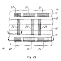
- FIG. 2a and 2B illustrate a greatly enlarged view of a substrate level, and the contact and conductor levels which overly the substrate level, respectively, of a four cells of the EEPROM integrated circuit.
- Byte erase line 14 of the portion of circuits of Figures 2A and 2B is a buried conductive line, such a doped n+ region of the substrate buried under a thick oxide, as will be further illustrated in the cross-sectional views of Figures 3 and 4.
- Bit lines 15, 151 and 152 are buried bit lines, also, for example n+ doped lines under thick oxide layers, which also act as source/drain regions of the pass transistors and storage transistors of the memory cells, as will be seen.
- Patterned thick field oxide regions 26 isolate the word erase line 14 and bit lines 15, 151, and 152 except in areas 31, areas 32 and areas 33 which allow the word erase transistors, pass transistors, and storage transistors, respectively, to be formed.
- Contact hole 23 allows contact to be made from buried line 34, which forms a source/drain region of the word-erase transistor, to control gate line 17.
- Tunnel windows 24 are cut through the thick oxide layers over buried n+ lines 35, which form source/drain regions of pass transistors 12-12n and storage transistors 13-13n. These tunnel windows 24 may be patterned and etched in accordance with any of several known fabrication methods including self-aligning methods presently developed. The critical parameter of these tunnel windows 24 is that the oxide thickness above buried n+ regions 28 must be thin enough to allow the well known tunneling phenomena to occur for writing and/or erasing to the storage transistors 13-13n.
- Word lines 16 which may be formed from a second level polysilicon layer, extend in a horizontal direction, as shown, overlying the substrate level and forming the gates of word erase transistor 11 above area 31 and forming the gates of pass transistors 12-12n over areas 32.
- Control gate lines 17 may also be formed from the second polysilicon level. These lines 17 also extend in a horizontal direction as shown, overlying floating gate regions 21, with insulating layer (e.g. silicon dioxide) there between. These lines 17 form the control gates of storage transistors 13-13n.
- insulating layer e.g. silicon dioxide
- Substrate 35 which may be single-crystal silicon, doped as required with p-type impurities, underlies the circuit.
- Buried n+ region 14 lies beneath thick oxide region 29 forming word-erase line 14 and a source/drain region of word erase transistor 11 at area 31, as shown in Figure 4.
- Thick field oxide regions 26 isolate buried n+ regions and separate word lines 16 from the substrate regions.
- Buried n+ region 34 acts as a source/drain region of word erase transistor 11, as shown in figure 4 and is covered by a thick oxide region. Contact hole 23 is etch through this thick oxide to the buried n+ region 34.
- Buried n+ regions 15, 151 and 152 also underlie thick oxide regions 29 and form buried bit lines 15, 151 and 152 and source/drain regions for the pass transistors 12-12n and storage transistors 13-13n.
- Buried n+ regions 28 also underlie thick oxide regions and form the other source/drain regions for pass transistors 12-12n and storage transistors 13-13n and electrically connect cell pairs of these transistors, e.g. pass transistor 12 to storage transistor 13, from source/drain to source/drain.
- the thick oxide regions above buried n+ regions 28 has a tunnel hole 24 etched through to the n+ region; a very thin layer of oxide or other insulator is then formed over the n+ region.
- a first level polysilicon layer is patterned and etched to form floating gates 21 and strap isolation regions 25.
- the floating gates 21 (storage gates) extend into tunnel window holes 24 and overly regions 33 to form the floating gates (storage gates) of storage transistors 13-13n.
- the second conducting layer e.g. polysilicon
- word lines 16 also form the gates of word erase transistor 11 and pass transistors 12-12n.
- Control gate lines 17 also form the control gates of storage transistors 13-13n.
- Conductive strap 22 extends into contact window 23 and into contact window 36 to electrically contact control gate line 17. Although strap 22 is shown overlying control gate lines 17, this strap 22 may also underlie the control gate lines 17. Conductive strap 22 may be metallic, for example, aluminum and is patterned and etched by well known techniques.
- a word-erase transistor 11 is formed across area 31 from word-erase lines 14 to buried n+ regions 34 with word lines 16 acting as gates of the word-erase transistor.
- the source-drain region of word-erase transistors 11 formed by buried n+ region 34 is then electrically strapped to the control gates of a number n of storage transistors 13-13n by control gate line 17, thus controlling a word erase of n storage transistors 13.
- FIG. 2a and 2b and descriptions show only a portion of an EEPROM array, according to the invention, comprising two word erase transistors, each controlling the erase mode of two memory cells.
- Each memory cell shown consists of a pass transistor and storage transistor pair. Therefore, a total of four memory cells are shown in the segment of the EEPROM integrated circuit depicted in Figures 2A and 2B.
- an EEPROM array according to the instant invention would include thousands or millions of memory cells and associated control circuitry, as is known in the art, such as row decoders and column decoders and read/write select circuitry.
Landscapes
- Semiconductor Memories (AREA)
- Non-Volatile Memory (AREA)
Applications Claiming Priority (2)
| Application Number | Priority Date | Filing Date | Title |
|---|---|---|---|
| US382607 | 1989-07-19 | ||
| US07/382,607 US5029139A (en) | 1989-07-19 | 1989-07-19 | Word erasable buried bit line EEPROM |
Publications (2)
| Publication Number | Publication Date |
|---|---|
| EP0409042A2 true EP0409042A2 (de) | 1991-01-23 |
| EP0409042A3 EP0409042A3 (en) | 1992-05-27 |
Family
ID=23509705
Family Applications (1)
| Application Number | Title | Priority Date | Filing Date |
|---|---|---|---|
| EP19900113113 Withdrawn EP0409042A3 (en) | 1989-07-19 | 1990-07-10 | Word erasable buried bit line eeprom |
Country Status (5)
| Country | Link |
|---|---|
| US (1) | US5029139A (de) |
| EP (1) | EP0409042A3 (de) |
| JP (1) | JPH03136367A (de) |
| KR (1) | KR100198770B1 (de) |
| CN (1) | CN1051448A (de) |
Cited By (2)
| Publication number | Priority date | Publication date | Assignee | Title |
|---|---|---|---|---|
| EP0443610A3 (en) * | 1990-02-23 | 1994-10-05 | Toshiba Kk | Nonvolatile semiconductor memory device |
| EP0962982A1 (de) * | 1998-06-03 | 1999-12-08 | STMicroelectronics S.r.l. | Schaltungsstruktur für Byte-Löschbare EEPROMs |
Families Citing this family (2)
| Publication number | Priority date | Publication date | Assignee | Title |
|---|---|---|---|---|
| US5999443A (en) * | 1997-02-01 | 1999-12-07 | Holtek Semiconductor Inc. | Low-voltage triple-well non-volatile semiconductor memory |
| CN102315249A (zh) * | 2011-10-15 | 2012-01-11 | 中国电子科技集团公司第五十八研究所 | 薄外延片上抗辐射eeprom芯片的抗esd器件结构 |
Family Cites Families (3)
| Publication number | Priority date | Publication date | Assignee | Title |
|---|---|---|---|---|
| US4408306A (en) * | 1981-09-28 | 1983-10-04 | Motorola, Inc. | Column and row erasable EEPROM |
| US4763305A (en) * | 1985-11-27 | 1988-08-09 | Motorola, Inc. | Intelligent write in an EEPROM with data and erase check |
| US4698900A (en) * | 1986-03-27 | 1987-10-13 | Texas Instruments Incorporated | Method of making a non-volatile memory having dielectric filled trenches |
-
1989
- 1989-07-19 US US07/382,607 patent/US5029139A/en not_active Expired - Fee Related
-
1990
- 1990-07-10 EP EP19900113113 patent/EP0409042A3/en not_active Withdrawn
- 1990-07-18 JP JP2190363A patent/JPH03136367A/ja active Pending
- 1990-07-18 KR KR1019900010879A patent/KR100198770B1/ko not_active Expired - Fee Related
- 1990-07-18 CN CN90104790A patent/CN1051448A/zh active Pending
Cited By (3)
| Publication number | Priority date | Publication date | Assignee | Title |
|---|---|---|---|---|
| EP0443610A3 (en) * | 1990-02-23 | 1994-10-05 | Toshiba Kk | Nonvolatile semiconductor memory device |
| EP0962982A1 (de) * | 1998-06-03 | 1999-12-08 | STMicroelectronics S.r.l. | Schaltungsstruktur für Byte-Löschbare EEPROMs |
| US6445031B1 (en) | 1998-06-03 | 2002-09-03 | Stmicroelectronics S.R.L. | Byte-switch structure for EEPROM memories |
Also Published As
| Publication number | Publication date |
|---|---|
| KR910003675A (ko) | 1991-02-28 |
| EP0409042A3 (en) | 1992-05-27 |
| US5029139A (en) | 1991-07-02 |
| KR100198770B1 (ko) | 1999-06-15 |
| JPH03136367A (ja) | 1991-06-11 |
| CN1051448A (zh) | 1991-05-15 |
Similar Documents
| Publication | Publication Date | Title |
|---|---|---|
| US5399891A (en) | Floating gate or flash EPROM transistor array having contactless source and drain diffusions | |
| US5654917A (en) | Process for making and programming a flash memory array | |
| US5698879A (en) | Nonvolatile semiconductor memory device | |
| EP0639860B1 (de) | Nichtflüchtiger Halbleiterspeicher | |
| US4580247A (en) | Semiconductor floating gate memory cell | |
| US5508544A (en) | Three dimensional FAMOS memory devices | |
| US6285574B1 (en) | Symmetric segmented memory array architecture | |
| EP0550404A1 (de) | Verfahren zur Herstellung einer kapazitiven Kupplungsvorrichtung, insbesondere für einen EEPROM | |
| US20010001491A1 (en) | Semiconductor memory device having memory cells each having a conductive body of booster plate and a method for manufacturing the same | |
| EP0573164A1 (de) | Mit allen Funktionen ausgestattete hochintegrierte EEPROM-Zelle mit Poly-Tunnel-Zwischenstück und Herstellungsverfahren | |
| US6031771A (en) | Memory redundancy circuit using single polysilicon floating gate transistors as redundancy elements | |
| US5321288A (en) | Nonvolatile memory array in which each cell has a single floating gate having two tunnelling windows | |
| EP0665593B1 (de) | Halbleitervorrichtung | |
| US5273926A (en) | Method of making flash EEPROM or merged FAMOS cell without alignment sensitivity | |
| EP0946988B1 (de) | Speicherredundanzschaltung, die einzelne polysilizium-schwebegattertransistoren als redundanzelemente verwendet | |
| US6327182B1 (en) | Semiconductor device and a method of operation the same | |
| US5012446A (en) | Large-scale EPROM memory with a high coupling factor | |
| US6235581B1 (en) | Floating gate memory structure and method for forming a low resistance continuous source line | |
| KR100241523B1 (ko) | 플래쉬 메모리 소자 및 이를 이용한 프로그램, 소거 및 독출방법 | |
| KR100706789B1 (ko) | 비휘발성 메모리 소자 | |
| US5029139A (en) | Word erasable buried bit line EEPROM | |
| US5134449A (en) | Nonvolatile memory cell with field-plate switch | |
| US5032533A (en) | Method of making a nonvolatile memory cell with field-plate switch | |
| US5147816A (en) | Method of making nonvolatile memory array having cells with two tunelling windows | |
| KR100665413B1 (ko) | 반도체 디바이스 |
Legal Events
| Date | Code | Title | Description |
|---|---|---|---|
| PUAI | Public reference made under article 153(3) epc to a published international application that has entered the european phase |
Free format text: ORIGINAL CODE: 0009012 |
|
| AK | Designated contracting states |
Kind code of ref document: A2 Designated state(s): DE FR GB IT NL |
|
| PUAL | Search report despatched |
Free format text: ORIGINAL CODE: 0009013 |
|
| AK | Designated contracting states |
Kind code of ref document: A3 Designated state(s): DE FR GB IT NL |
|
| 17P | Request for examination filed |
Effective date: 19921130 |
|
| 17Q | First examination report despatched |
Effective date: 19940228 |
|
| STAA | Information on the status of an ep patent application or granted ep patent |
Free format text: STATUS: THE APPLICATION IS DEEMED TO BE WITHDRAWN |
|
| 18D | Application deemed to be withdrawn |
Effective date: 19940830 |