EP0409188A2 - Dispositif d'affichage matriciel en couleur et méthode pour sa conception - Google Patents
Dispositif d'affichage matriciel en couleur et méthode pour sa conception Download PDFInfo
- Publication number
- EP0409188A2 EP0409188A2 EP90113727A EP90113727A EP0409188A2 EP 0409188 A2 EP0409188 A2 EP 0409188A2 EP 90113727 A EP90113727 A EP 90113727A EP 90113727 A EP90113727 A EP 90113727A EP 0409188 A2 EP0409188 A2 EP 0409188A2
- Authority
- EP
- European Patent Office
- Prior art keywords
- color
- display
- grating
- diffraction grating
- dimensional
- Prior art date
- Legal status (The legal status is an assumption and is not a legal conclusion. Google has not performed a legal analysis and makes no representation as to the accuracy of the status listed.)
- Granted
Links
- 239000011159 matrix material Substances 0.000 title claims abstract description 60
- 238000000034 method Methods 0.000 title claims description 13
- 239000004973 liquid crystal related substance Substances 0.000 claims abstract description 16
- 230000003287 optical effect Effects 0.000 claims abstract description 12
- 238000005070 sampling Methods 0.000 claims description 17
- 239000000758 substrate Substances 0.000 claims description 8
- 239000011521 glass Substances 0.000 claims description 7
- 230000005540 biological transmission Effects 0.000 claims description 4
- 239000003086 colorant Substances 0.000 claims description 3
- 230000000007 visual effect Effects 0.000 claims description 2
- 238000001514 detection method Methods 0.000 claims 1
- 235000019557 luminance Nutrition 0.000 description 14
- 239000000463 material Substances 0.000 description 7
- 108010010803 Gelatin Proteins 0.000 description 5
- 229920000159 gelatin Polymers 0.000 description 5
- 239000008273 gelatin Substances 0.000 description 5
- 235000019322 gelatine Nutrition 0.000 description 5
- 235000011852 gelatine desserts Nutrition 0.000 description 5
- 230000008569 process Effects 0.000 description 4
- 238000012545 processing Methods 0.000 description 4
- 238000000926 separation method Methods 0.000 description 4
- 238000013461 design Methods 0.000 description 3
- 238000001914 filtration Methods 0.000 description 3
- 229920002120 photoresistant polymer Polymers 0.000 description 2
- 238000009877 rendering Methods 0.000 description 2
- 238000012546 transfer Methods 0.000 description 2
- 230000002238 attenuated effect Effects 0.000 description 1
- 230000008901 benefit Effects 0.000 description 1
- 238000009125 cardiac resynchronization therapy Methods 0.000 description 1
- 230000008859 change Effects 0.000 description 1
- 238000000576 coating method Methods 0.000 description 1
- 230000001419 dependent effect Effects 0.000 description 1
- 238000009795 derivation Methods 0.000 description 1
- 230000001066 destructive effect Effects 0.000 description 1
- 238000009792 diffusion process Methods 0.000 description 1
- 238000002474 experimental method Methods 0.000 description 1
- 238000009499 grossing Methods 0.000 description 1
- 230000006872 improvement Effects 0.000 description 1
- 238000004519 manufacturing process Methods 0.000 description 1
- 239000000203 mixture Substances 0.000 description 1
- 239000003973 paint Substances 0.000 description 1
- 230000000737 periodic effect Effects 0.000 description 1
- 230000010363 phase shift Effects 0.000 description 1
- 238000002922 simulated annealing Methods 0.000 description 1
- 125000006850 spacer group Chemical group 0.000 description 1
- 230000003068 static effect Effects 0.000 description 1
- 238000012360 testing method Methods 0.000 description 1
- 230000007704 transition Effects 0.000 description 1
- XLYOFNOQVPJJNP-UHFFFAOYSA-N water Substances O XLYOFNOQVPJJNP-UHFFFAOYSA-N 0.000 description 1
Images







Classifications
-
- G—PHYSICS
- G02—OPTICS
- G02F—OPTICAL DEVICES OR ARRANGEMENTS FOR THE CONTROL OF LIGHT BY MODIFICATION OF THE OPTICAL PROPERTIES OF THE MEDIA OF THE ELEMENTS INVOLVED THEREIN; NON-LINEAR OPTICS; FREQUENCY-CHANGING OF LIGHT; OPTICAL LOGIC ELEMENTS; OPTICAL ANALOGUE/DIGITAL CONVERTERS
- G02F1/00—Devices or arrangements for the control of the intensity, colour, phase, polarisation or direction of light arriving from an independent light source, e.g. switching, gating or modulating; Non-linear optics
- G02F1/01—Devices or arrangements for the control of the intensity, colour, phase, polarisation or direction of light arriving from an independent light source, e.g. switching, gating or modulating; Non-linear optics for the control of the intensity, phase, polarisation or colour
- G02F1/13—Devices or arrangements for the control of the intensity, colour, phase, polarisation or direction of light arriving from an independent light source, e.g. switching, gating or modulating; Non-linear optics for the control of the intensity, phase, polarisation or colour based on liquid crystals, e.g. single liquid crystal display cells
- G02F1/133—Constructional arrangements; Operation of liquid crystal cells; Circuit arrangements
- G02F1/1333—Constructional arrangements; Manufacturing methods
- G02F1/1335—Structural association of cells with optical devices, e.g. polarisers or reflectors
-
- G—PHYSICS
- G02—OPTICS
- G02F—OPTICAL DEVICES OR ARRANGEMENTS FOR THE CONTROL OF LIGHT BY MODIFICATION OF THE OPTICAL PROPERTIES OF THE MEDIA OF THE ELEMENTS INVOLVED THEREIN; NON-LINEAR OPTICS; FREQUENCY-CHANGING OF LIGHT; OPTICAL LOGIC ELEMENTS; OPTICAL ANALOGUE/DIGITAL CONVERTERS
- G02F1/00—Devices or arrangements for the control of the intensity, colour, phase, polarisation or direction of light arriving from an independent light source, e.g. switching, gating or modulating; Non-linear optics
- G02F1/01—Devices or arrangements for the control of the intensity, colour, phase, polarisation or direction of light arriving from an independent light source, e.g. switching, gating or modulating; Non-linear optics for the control of the intensity, phase, polarisation or colour
- G02F1/13—Devices or arrangements for the control of the intensity, colour, phase, polarisation or direction of light arriving from an independent light source, e.g. switching, gating or modulating; Non-linear optics for the control of the intensity, phase, polarisation or colour based on liquid crystals, e.g. single liquid crystal display cells
- G02F1/133—Constructional arrangements; Operation of liquid crystal cells; Circuit arrangements
- G02F1/1333—Constructional arrangements; Manufacturing methods
- G02F1/1335—Structural association of cells with optical devices, e.g. polarisers or reflectors
- G02F1/133504—Diffusing, scattering, diffracting elements
-
- G—PHYSICS
- G02—OPTICS
- G02B—OPTICAL ELEMENTS, SYSTEMS OR APPARATUS
- G02B5/00—Optical elements other than lenses
- G02B5/18—Diffraction gratings
- G02B5/1842—Gratings for image generation
-
- G—PHYSICS
- G02—OPTICS
- G02F—OPTICAL DEVICES OR ARRANGEMENTS FOR THE CONTROL OF LIGHT BY MODIFICATION OF THE OPTICAL PROPERTIES OF THE MEDIA OF THE ELEMENTS INVOLVED THEREIN; NON-LINEAR OPTICS; FREQUENCY-CHANGING OF LIGHT; OPTICAL LOGIC ELEMENTS; OPTICAL ANALOGUE/DIGITAL CONVERTERS
- G02F2201/00—Constructional arrangements not provided for in groups G02F1/00 - G02F7/00
- G02F2201/30—Constructional arrangements not provided for in groups G02F1/00 - G02F7/00 grating
- G02F2201/305—Constructional arrangements not provided for in groups G02F1/00 - G02F7/00 grating diffraction grating
Definitions
- the present invention is related to a color matrix display apparatus according to the preamble of claim 1 and to a method for designing it.
- this invention is directed to the area of optical reconstruction filters for color mosaic (matrix) displays as e.g. flat panel liquid crystal displays.
- Segment 3a of Figure 3 shows an ideal signal (image) which is to be processed.
- An initial filter, the anti-aliasing filter, 3b, is used at the outset to limit the bandwidth of the ideal signal to frequencies the processing system can handle. Frequencies that are too high result in spurious noise and moire patterns.
- the cutoff frequency of the anti-aliasing filter is determined, by sampling theory, to be at one-half of the frequency the system uses to sample the incoming signal.
- the system in the two-dimensional case consist of an image generator and color matrix display device. This cutoff frequency is commonly referred to as the Nyquist frequency.
- the output of the anti-aliasing filter is the actual signal (image) to be entered into the system, as shown at section 3c.
- the signal (image) is then digitized through an A/D converter (image generator), shown at section 3d, and is ready to be transferred to the rest of the system.
- the digital signal (image) passes through a D/A converter, shown at section 3e.
- the output waveform of the D/A, shown at section 3f is a signal (image), with undesirable high frequency noise present.
- the noise is due to the underlying sampling grid and results from an incomplete reconstruction process.
- the signal is passed through another filter, the reconstruction filter, shown at section 3g, with its cutoff again determined by the Nyquist criterion.
- the output shape shown at section 3h is identical to the system input at section 3c.
- All color matrix displays intentionally or not, have relied on one of two types of optical reconstruction filters; 1) the eye itself with its associated low pass filter characteristics, or 2) a diffuse, or scattering, optical surface.
- the eye as a reconstruction filter does not work satisfactorily for current flat panel display resolutions.
- present color matrix displays typically have pixels 0,015 to 0,02 nm (6 to 8 mils) across.
- Human factors experiments have determined these pixel sizes result in sampling grids all too easily seen by the eye.
- the frequency content of the color matrix display structure, the display sampling grid is clearly well within the bandpass characteristics of human vision.
- the eye cannot filter out spatial frequencies this low at typical viewing distances.
- the resolution of color matrix displays must increase significantly before the eye alone will be a sufficient low pass filter. This, however, is the reconstruction filter most often used for color matrix display applications.
- a diffuse scattering surface scatters the light, giving it optical low pass filter characteristics. The more scattering the surface accomplishes, the more diffuse the filter, and the more it smooths the image.
- a common example is the diffuse picture glass frequently placed over photographs to reduce specular reflections.
- the invention is a diffraction grating filter with defined spatial frequency passband characteristics, used to eliminate noise generated by color matrix dot structure.
- the invention uses sampling theory to determine the frequency capability of the particular display. This is found by determining the Nyquist boundaries in two dimensions covering the surface of the display. The invention applies these two-dimensional boundaries to define the extent of traditional interpolation functions. Finally, the invention physically embodies these interpolation functions in the form of a phase diffraction grating in conjunction with the filter characteristics of the eye.
- the phase diffraction grating (may be a binary step type) is then applied over the surface of a color mosaic display to alter the point spread function of each pixel.
- the luminance contained in each sample is distributed as a function of the distance from the sample point as defined by the interpolation function. Accordingly, information contained in each sample is added with information of surrounding samples of like primary hue to provide continuous luminance functions for each primary color. A higher fidelity representation of the desired output signal results.
- Continuity of the image function can be made through 1st, 2nd and higher order derivatives, depending on which interpolation function is selected to be embodied in the diffraction grating. Recognizing the lattice structure of each primary color is a key element of this invention. It can be applied to color mosaic patterns in general, including stripe, diagonal, delta, and quad pixel patterns.
- the invention provides continuity of the luminance functions of each primary hue on a color mosaic display in order to improve the image quality of sampled images.
- a diffraction grating used as an optical reconstruction filter for color matrix displays uses the phenomenon of diffraction to filter the image, instead of using scattering.
- the diffraction grating breaks each pixel image up into the various diffraction orders as it passes through the grating. These orders can be made to overlap and fall off in intensity, as shown in Figure 5.
- the diffracted pixels overlap and cause interpolation among the pixels of like color, getting rid of the high spatial frequency grid noise.
- the exact interpolation function used is determined by the position and intensity of the diffracted orders, which is, in turn, determined by the geometry and period of the diffraction grating structure, and the refractive index of the material.
- diffraction grating as a reconstruction filter is very advantageous for display applications.
- reflections from the filter are specular instead of diffuse. These reflections still need to be handled, but they are easier to manage than diffuse reflections. Specular reflections can be cut down to less than 0.5% with standard optical anti-reflection coatings. Destructive interference techniques can be used to cut the reflections down even further.
- the diffraction grating can be tailored to give the desired passband characteristics and interpolation functions.
- the passband characteristics of the filter need not be constant over direction. The almost infinite range of order intensities and positioning gives the designer freedom to choose the best interpolation functions for the job.
- Figure 12 shows some common interpolation functions, all of which would smooth the flat panel images.
- the surface profile of the diffraction grating can be designed to create these interpolation functions. This allows the reconstruction filter to be tailored to the exact structure of the color matrix display.
- the invention is easily incorporated into the color matrix display structure.
- the filter is etched in glass and can be bonded to the front of the panel or even made in the flat panel substrate glass.
- An example of the structure of the flat panel color matrix display together with the diffraction grating reconstruction filter proximate in front of it is shown in Figure 18.
- the invention is a diffraction grating, with defined spatial frequency passband characteristics, to be used as a reconstruction filter for color matrix displays, especially liquid crystal including active matrix liquid crystal flat panel color matrix displays such as is described in EP-A 0 316 708.
- the invention interpolates among luminance values stored at each pixel site and, in concert with the low pass characteristics of the eye, renders a continuous image in the domain of each primary color.
- a diffraction grating filter is used to reduce flat panel image artifacts such as gaps, staircasing and color aliasing. This filter which is placed over a flat display panel of hundreds of pixels, smooths and precisely spreads the luminance profile of each pixel.
- the diffraction grating has several characteristics which make it useful for display applications including a first that the light spread function is variable over direction, and a second that the non-scattering reflection characteristics make reflections easier to control.
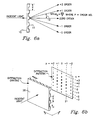
- a diffraction grating 10 herein also referred to as a diffractive diffuser.
- the diffractive diffuser uses the phenomenon of diffraction, which is incident light breaking up into "orders" after passing through a periodic edge 11 of the diffraction grating.
- the zero, first and second orders are shown in the figure.
- the image passing straight through the filter is called the zero order.
- the images on either side of the zero order are the +1 and the -1 order.
- the next images on either side are the +2 and the -2 order.
- FIG 6B there is shown a two dimensional diffraction grating 20 having grating intervals x and y.
- the diffraction pattern of light from the incident light beam is two dimensional as shown on plane 21.
- the letters p and q represent the order numbers in the two dimensions x and y. In actual case more than two or three orders may be used giving much smoother final image.
- the position and intensity of the various orders are determined by the geometry and period of the diffraction grating structure and the index variation of the material.
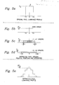
- the grating will be made such that the orders overlap and fall off in intensity, creating an image much more gaussian than the original "step" image of the pixel, as shown in Figure 5a-e. These diffracted pixels will overlap and cause interpolation between pixels.
- the characteristics of a diffraction grating can be designed to be a function of direction, so the light spread function can be tailored to the flat panel pixel pattern.
- FIG. 5 where I represents intensity, and particularly to Figure 5a there is illustrated the original pixel image having an intensity represented by height I o and horizontal dimensions from -a to +a.
- the diffracted pixel orders change pixel luminance profile.
- Figures 5b, 5c and 5d illustrate the zero order, +1 and -1 orders and the +2 and -2 orders, respectively.
- Figure 5b illustrates the zero order with an intensity of 2I o /5 and dimensions from -a to +a.
- Figure 5c illustrates the +1 and -1 orders and shows an intensity of I o /5 with horizontal dimension of 3a (that is from -3/2a to +3/2a).
- Figure 5d illustrates the +2 and -2 orders and shows an intensity of I o /10 and dimensions of 4a.
- Figure 5e illustrates the diffracted pixel image. In actual case, more than two orders may be used giving much smoother final image.
- diffraction gratings There are several different types of diffraction gratings. These include amplitude or phase types, and transmissive or reflective types. There are several manufacturing techniques, including holographic, ruled, and photolithographic.
- a phase transmission grating is preferred because it has the highest transmission. It may be a binary step type.
- the active diffractive material is transparent, with thickness variation across the surface.
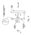
- Figure 4 is illustrative of how the image of a point on the flat image panel 30 gets spread out by a diffraction grating 31. The grating 31 will be positioned in front of the panel 30 as shown in Figure 4, with the viewer 32 looking at the diffracted image.
- a two axis grating will be used.
- the axes of the grating is preferably oriented to the major axes of the flat panel pixel pattern.
- the profile of the grating in ⁇ and y is determined such that the luminance of same color pixels is interpolated in each direction.
- the distance between same color pixels is usually not the same in both axes. This distance is also different for different pixel layouts, such as the diagonal layouts versus the quad layouts.
- the grating profile is therefore tailored to a panel with a specific pixel size, spacing and layout. In one embodiment the grating is designed specifically for the Hosiden 0,017 mm (6.7 mil) diagonal mosaic panel.
- the diffraction grating 31 is effective to spread out the luminance profile of each pixel, interpolating between same color pixel images.
- the final pixel luminance is a design factor. It has been determined that the actual shape of the interpolation function is not as critical as the amount of interpolation used to smooth out the flat panel image. For example, if the interpolation function spans several pixels, colors of individual pixels will blend together more effectively with neighboring pixels to alleviate a common complaint of liquid crystal flat panel displays that they show an objectionable amount of color bonding on misconvergence.
- a current problem of the prior art is that pixel size and patterns result in a pointillist or dotted presentation of the image.
- Using any of a linear or gaussian or cubic B-spline shape for interpolation can eliminate or minimize the dotted appearance and produce a significant advance in the quality of the image. Care must be exercised so as to not introduce too much interpolation othervise excessive blurring or defocussing will be perceived. Fortunately, the extent of the interpolation can easily be controlled by altering the spacing between the diffraction grating 31 and the display panel 30.
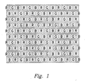
- Figure 1 shows the individual red, green, and blue pixels of a typical color matrix display.
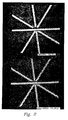
- Figure 2 illustrates the pixel structure artifacts which can occur from this type of discrete image display system. Jagged transitions, on what are intended to be smooth lines detract from positional accuracy and, in the case of moving symbology, lines appear to move in a jumpy, discrete fashion. Ideally, the flat panel color matrix display would paint smoothly shaped symbols, which move in a smooth, analog manner and exhibit color purity.
- the diffraction grating used as an optical reconstruction filter, is used to obtain this smooth image on a color matrix display. The manner in which the diffraction grating is used as a reconstruction filter for color matrix displays is explained in the following paragraphs.
- Determining the desired spatial frequency passband characteristics of the reconstruction filter is key, and begins with recognizing the underlying lattice structure of the color matrix display to be used.
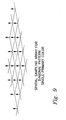
- Figure 8 shows a diagonal matrix pattern with the red primary lattice structure superimposed. This lattice structure determines the spatial sampling array of the primary color, as shown in Figure 9.
- the spatial sampling array for all three primary colors is the same.
- the spatial frequency lattice of the color matrix display is determined next. This is found by taking the Fourier transform of the spatial sampling array.
- Nyquist theory is used to determine the bandpass characteristics of the reconstruction filter.
- Nyquist sampling theory states that the maximum frequency which can be displayed on a color matrix display, without creating aliasing, is one half of the sampling frequency.
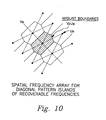
- the boundaries for maximum displayable frequencies therefore fall midway between the lattice points of the spatial frequency array. These boundaries, called the Nyquist boundaries, are shown in Figure 10 for the diagonal matrix pattern.
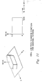
- the Nyquist boundaries define the maximum frequency capability of the color mosaic in all directions. Therefore, the transfer function of the ideal bandpass filter for the diagonal pattern is as shown in Figure 11.
- the next step is to determine the interpolation function to be used, with the extent of interpolation defined by the Nyquist boundaries.
- Figure 12 shows some possible interpolation functions which give acceptable results.
- the triangle function is one of the simplest, whereas some of the other functions, such as the cubic B-spline, give more accurate results.
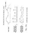
- Figure 13A gives an example of a one-dimensional reconstruction using the triangle function. The higher order interpolations give better reconstruction of the signal. Ideally the sinc function (of the form sin(x)/x) would be used, as shown in Figure 13B.
- the diffraction grating optical reconstruction filter is then designed to create the corresponding point spread function (PSF).
- the PSF of the diffraction grating is determined by the position and intensity of the various diffracted orders.
- the position and intensity of the diffracted orders is determined by the surface profile of the diffraction grating.
- the equations which relate the position and intensity of diffracted orders to the surface profile of a diffraction grating are standard diffraction equations.
- the surface profile of the grating controls the resulting PSF of the grating.
- the PSF is varied and can be tailored to deliver the desired interpolation function. There are several ways of accomplishing this, including empirical, simulated annealing, or holographic techniques.
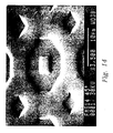
- Figure 14 shows one embodiment of the invention, a phase diffraction grating designed for the RGBY quad pixel arrangement.
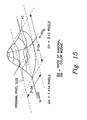
- the interpolation function which was chosen for this application approximates the cubic B-spline, as shown in Figure 15.
- Figure 15 shows the intensity profile of a pixel from a diagonal color mosaic display after it has undergone a cubic B-spline interpolation. This may also be described as the resultant pixel luminance profile when cubic B-spline interpolation is applied to diagonal color mosaic pattern.
- the orientation of the interpolation function can also be changed if desired.
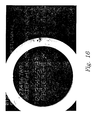
- Figure 16 shows this grating over a panel and illustrates the interpolation and resulting smoothing of the sampled image.
- the diffraction grating reconstruction filter can be used for any of the pixel patterns used with color matrix displays. In each case, by tailoring the filter to the lattice structure as explained above, the full frequency capability of each particular pattern is used. Frequencies beyond this capability are eliminated. The result is enhanced image quality on color matrix displays.
- Figure 8 there is shown the major axes a and b and the separation between same color pixels R, G, and B of diagonal color mosaic pattern.
- the interpolation function is oriented along the plus and minus 45 degree axes of the diagonal mosaic pattern.
- the orientation of the interpolation function can also be changed to test questions about preferred axes of orientation of the target image.
- static characters for example, which are predominately rendered with vertical and horizontal strokes
- n p,q the efficiency of each order.
- w(x,y) is the phase shift introduced by passage through the grating
- n o the refractive index of the surrounding medium
- n1 the refractive index of the grating material
- s(x,y) is the function which describes the surface profile of the diffraction grating.
- Figure 17 One process for fabricating a diffraction grating with dichromated gelatin using photolithographic techniques is illustrated in Figure 17.
- a layer of photoresist material such as dichromated gelatin, is spun or otherwise deposited onto a glass substrate. Then through a mask the photoresist material is exposed with uv light. The areas which have been exposed are washed away with water, leaving a surface profile of dichromated gelatin.
- the mask used to prepare gratings has 100 lines/mm in both the x and y directions.
- Figure 18 shows the flat panel structure 41 and how the diffraction grating reconstruction filter (diffuser) 42 can be placed.
- the diffraction diffuser 42 here takes the form of a thin glass substrate, with a phase relief structure deposited upon it, placed over the last polarizer 43 in the flat panel stack.
- Beneath polarizer 43 is an upper substrate color filter 44, a common electrode 45, a spacer 46, the liquid crystal material 47 and the flat panel display 48 on the lower substrate 49.
- Polarizer 50 may be positioned beneath the lower substrate 49.
- Backlighting 51 is provided.
- a magnified section 52 of the diffuser 42 is shown in the balloon 53.
- FIG. 19 A drawing of a photograph of a grating fabricated with the 100 line/mm mask is shown in Figure 19. The circles are "wells" where the dichromated gelatin has been removed.
- Figure 20 shows the pattern created when a laser beam is passed through the grating. large throw distance was used to spread out the orders and illustrate their relative efficiencies. For flat panel use the diffraction grating is closely spaced to the panel so that the orders are all overlapping.
- the present invention has entailed how one goes about specifying the filter requirements for a diffraction grating to operate as an optical reconstruction filter, when a particular flat panel liquid crystal color mosaic pattern is given. There is specified a method of determining filter cutoff requirements given any pixel pattern on the color matrix display; and there is specified the filter cutoff requirements in terms of each primary color lattice in the mosaic.
- the present invention is of a design to permit maximum use of available color mosaic spatial frequency capacity.
Landscapes
- Physics & Mathematics (AREA)
- Nonlinear Science (AREA)
- General Physics & Mathematics (AREA)
- Optics & Photonics (AREA)
- Mathematical Physics (AREA)
- Chemical & Material Sciences (AREA)
- Crystallography & Structural Chemistry (AREA)
- Diffracting Gratings Or Hologram Optical Elements (AREA)
- Liquid Crystal (AREA)
Applications Claiming Priority (2)
| Application Number | Priority Date | Filing Date | Title |
|---|---|---|---|
| US382514 | 1989-07-20 | ||
| US07382514 US5046827C1 (en) | 1989-07-20 | 1989-07-20 | Optical reconstruction filter for color mosaic displays |
Publications (3)
| Publication Number | Publication Date |
|---|---|
| EP0409188A2 true EP0409188A2 (fr) | 1991-01-23 |
| EP0409188A3 EP0409188A3 (en) | 1991-12-27 |
| EP0409188B1 EP0409188B1 (fr) | 1995-12-13 |
Family
ID=23509293
Family Applications (1)
| Application Number | Title | Priority Date | Filing Date |
|---|---|---|---|
| EP90113727A Expired - Lifetime EP0409188B1 (fr) | 1989-07-20 | 1990-07-18 | Dispositif d'affichage matriciel en couleur et méthode pour sa conception |
Country Status (7)
| Country | Link |
|---|---|
| US (1) | US5046827C1 (fr) |
| EP (1) | EP0409188B1 (fr) |
| JP (1) | JP3184978B2 (fr) |
| KR (1) | KR100223380B1 (fr) |
| CA (1) | CA2020372C (fr) |
| DE (1) | DE69024120T2 (fr) |
| FI (1) | FI903645A7 (fr) |
Cited By (9)
| Publication number | Priority date | Publication date | Assignee | Title |
|---|---|---|---|---|
| EP0567995A1 (fr) * | 1992-04-28 | 1993-11-03 | Kuraray Co., Ltd. | Dispositif d'affichage d'image |
| EP0618473A3 (fr) * | 1993-03-31 | 1995-03-15 | Kuraray Co | Dispositif vidéo avec réseau de diffraction bi-dimensionnel. |
| EP0724168A1 (fr) * | 1995-01-28 | 1996-07-31 | Dr. Johannes Heidenhain GmbH | Réseau de phase |
| EP0698804A3 (fr) * | 1994-08-26 | 1998-09-02 | Omron Corporation | Dispositifs à cristaux liquides utilisant un filtre optique passe-bas et un polariseur |
| US6124920A (en) * | 1996-08-01 | 2000-09-26 | Sharp Kabushiki Kaisha | Optical device and directional display |
| US6147732A (en) * | 1994-08-26 | 2000-11-14 | Omron Corporation | Dot matrix-type display device with optical low-pass filter fixed to a member via an adhesive bonding |
| US7439683B2 (en) | 2003-05-21 | 2008-10-21 | Pure Depth Limited | Backlighting system for display screen |
| US9721378B2 (en) | 2001-10-11 | 2017-08-01 | Pure Depth Limited | Display interposing a physical object within a three-dimensional volumetric space |
| EP3396434A1 (fr) * | 2017-04-28 | 2018-10-31 | Samsung Display Co., Ltd. | Dispositif d'affichage, affichage électroluminescent organique et visiocasque |
Families Citing this family (68)
| Publication number | Priority date | Publication date | Assignee | Title |
|---|---|---|---|---|
| US5300942A (en) * | 1987-12-31 | 1994-04-05 | Projectavision Incorporated | High efficiency light valve projection system with decreased perception of spaces between pixels and/or hines |
| JPH03289692A (ja) * | 1990-04-06 | 1991-12-19 | Matsushita Electric Ind Co Ltd | 空間光変調素子及びこれを用いたホログラム画像情報記録装置 |
| DE4132902C2 (de) * | 1991-10-04 | 2001-08-02 | Optrex Europ Gmbh | Flüssigkristallanzeige |
| US5303085A (en) * | 1992-02-07 | 1994-04-12 | Rallison Richard D | Optically corrected helmet mounted display |
| US6097543A (en) | 1992-02-07 | 2000-08-01 | I-O Display Systems Llc | Personal visual display |
| WO1995021440A1 (fr) * | 1994-02-07 | 1995-08-10 | Virtual I/O, Inc. | Unite de visualisation depixelee |
| US5864326A (en) * | 1992-02-07 | 1999-01-26 | I-O Display Systems Llc | Depixelated visual display |
| US6219015B1 (en) * | 1992-04-28 | 2001-04-17 | The Board Of Directors Of The Leland Stanford, Junior University | Method and apparatus for using an array of grating light valves to produce multicolor optical images |
| JP3506144B2 (ja) * | 1992-10-19 | 2004-03-15 | ソニー株式会社 | 画像表示装置及び表示デバイス用光学フィルタ |
| US5526022A (en) | 1993-01-06 | 1996-06-11 | Virtual I/O, Inc. | Sourceless orientation sensor |
| US5757544A (en) * | 1993-03-09 | 1998-05-26 | Olympus Optical Co., Ltd. | Image display apparatus |
| EP0627644B1 (fr) * | 1993-06-01 | 2001-11-28 | Sharp Kabushiki Kaisha | Dispositif d'affichage d'image avec éclairage par l'arrière |
| JPH07104276A (ja) * | 1993-10-08 | 1995-04-21 | Olympus Optical Co Ltd | 液晶表示装置 |
| US5991087A (en) * | 1993-11-12 | 1999-11-23 | I-O Display System Llc | Non-orthogonal plate in a virtual reality or heads up display |
| US6160666A (en) | 1994-02-07 | 2000-12-12 | I-O Display Systems Llc | Personal visual display system |
| US5629784A (en) * | 1994-04-12 | 1997-05-13 | Ois Optical Imaging Systems, Inc. | Liquid crystal display with holographic diffuser and prism sheet on viewer side |
| US5550663A (en) * | 1994-05-24 | 1996-08-27 | Omron Corporation | Method of manufacturing optical low-pass filter |
| JPH0821991A (ja) * | 1994-07-08 | 1996-01-23 | Sony Corp | 画像表示装置 |
| US5737042A (en) * | 1994-08-31 | 1998-04-07 | Omron Corporation | Image display device with optical low-pass filter |
| US5903395A (en) | 1994-08-31 | 1999-05-11 | I-O Display Systems Llc | Personal visual display system |
| US5755501A (en) * | 1994-08-31 | 1998-05-26 | Omron Corporation | Image display device and optical low-pass filter |
| KR100207135B1 (ko) * | 1994-10-18 | 1999-07-15 | 니시무로 타이죠 | 반사형 액정표시소자 및 그 제조방법 |
| AU1682395A (en) * | 1995-01-18 | 1996-08-07 | Virtual I/O, Inc. | Speckle depixelator |
| US5682266A (en) * | 1995-04-05 | 1997-10-28 | Eastman Kodak Company | Blur filter for eliminating aliasing in electrically sampled images |
| US5991085A (en) | 1995-04-21 | 1999-11-23 | I-O Display Systems Llc | Head-mounted personal visual display apparatus with image generator and holder |
| JP2951264B2 (ja) * | 1995-05-24 | 1999-09-20 | 三洋電機株式会社 | 2次元映像/3次元映像互換型映像表示装置 |
| USD375495S (en) | 1995-07-20 | 1996-11-12 | Virtual I/O, Inc. | Head mounted display |
| JP3268625B2 (ja) * | 1995-08-11 | 2002-03-25 | シャープ株式会社 | 3次元画像表示装置 |
| JP3464570B2 (ja) * | 1995-08-21 | 2003-11-10 | 株式会社 日立ディスプレイズ | カラー液晶表示素子 |
| USD383455S (en) * | 1995-08-31 | 1997-09-09 | Virtual I/O, Inc. | Head mounted display with headtracker |
| US5721598A (en) * | 1995-12-26 | 1998-02-24 | Hughes Electronics | High efficiency, high color purity, on-axis holographic color filter and full-color liquid crystal display |
| CA2222031C (fr) * | 1996-03-25 | 2002-01-29 | Rainbow Displays, Inc. | Quadrillage d'ecrans plats possedant une fonction de correction des couleurs |
| IL118057A0 (en) * | 1996-04-29 | 1996-09-12 | Patir Research And Dev Limited | Optical phase element |
| US5696371A (en) * | 1996-05-23 | 1997-12-09 | Eastman Kodak Company | Diffractive/refractive lenslet array |
| US5751492A (en) * | 1996-06-14 | 1998-05-12 | Eastman Kodak Company | Diffractive/Refractive lenslet array incorporating a second aspheric surface |
| JP3683397B2 (ja) * | 1997-07-02 | 2005-08-17 | 富士写真フイルム株式会社 | カラー画像データ補間方法および装置 |
| KR100262825B1 (ko) * | 1997-08-13 | 2000-08-01 | 구자홍 | 투사형디스플레이장치 |
| US5903396A (en) * | 1997-10-17 | 1999-05-11 | I/O Display Systems, Llc | Intensified visual display |
| US5963284A (en) * | 1998-04-01 | 1999-10-05 | Ois Optical Imaging Systems, Inc. | LCD with diffuser having diffusing particles therein located between polarizers |
| KR100813321B1 (ko) | 2000-11-17 | 2008-03-12 | 딥 비디오 이미징 리미티드 | 디스플레이 기술의 개선방법 |
| KR100765308B1 (ko) * | 2001-03-17 | 2007-10-09 | 삼성전자주식회사 | 액정 표시 장치 |
| NZ511255A (en) * | 2001-04-20 | 2003-12-19 | Deep Video Imaging Ltd | Multi-focal plane display having an optical retarder and a diffuser interposed between its screens |
| WO2003004931A2 (fr) * | 2001-06-30 | 2003-01-16 | Samsung Electro-Mechanics Co., Ltd. | Retroeclairage utilisant un hologramme plat destine a un dispositif d'affichage plat |
| NZ514119A (en) | 2001-09-11 | 2004-06-25 | Deep Video Imaging Ltd | Improvement to instrumentation |
| US6636285B2 (en) | 2001-11-01 | 2003-10-21 | Motorola, Inc. | Reflective liquid crystal display with improved contrast |
| US7742239B2 (en) * | 2002-03-17 | 2010-06-22 | Puredepth Limited | Method to control point spread function of an image |
| EP1540407A4 (fr) * | 2002-07-15 | 2009-01-07 | Puredepth Ltd | Ecran video multicouche ameliore |
| KR20040013753A (ko) * | 2002-08-08 | 2004-02-14 | 삼성전자주식회사 | 기판 및 이를 포함하는 액정 표시 장치 |
| NZ521505A (en) | 2002-09-20 | 2005-05-27 | Deep Video Imaging Ltd | Multi-view display |
| JP4216577B2 (ja) * | 2002-12-20 | 2009-01-28 | シチズン電子株式会社 | 導光板 |
| US7414595B1 (en) | 2003-12-07 | 2008-08-19 | Advanced Simulation Displays Co. | Virtual mosaic wide field of view display system |
| WO2007091373A1 (fr) * | 2006-02-06 | 2007-08-16 | Nippon Telegraph And Telephone Corporation | Dispositif d'affichage en 3 dimensions et procede de presentation d'images |
| US8605017B2 (en) * | 2006-06-02 | 2013-12-10 | Samsung Display Co., Ltd. | High dynamic contrast display system having multiple segmented backlight |
| US20100033456A1 (en) * | 2007-05-14 | 2010-02-11 | Keisuke Yoshida | Display device and display method thereof |
| KR20100067085A (ko) * | 2007-08-22 | 2010-06-18 | 푸에뎁스 리미티드 | 멀티 컴포넌트 디스플레이용 인터스티셜 확산기의 위치 결정 |
| KR20090111583A (ko) * | 2008-04-22 | 2009-10-27 | 삼성전자주식회사 | 표시 장치 |
| JP5437886B2 (ja) * | 2009-04-06 | 2014-03-12 | 日東電工株式会社 | 液晶表示装置および集光素子付偏光板 |
| TWI551917B (zh) * | 2010-02-04 | 2016-10-01 | 群創光電股份有限公司 | 液晶面板模組與液晶顯示裝置 |
| TWI428666B (zh) * | 2010-02-04 | 2014-03-01 | Innolux Corp | 液晶面板模組、背光模組與液晶顯示裝置 |
| JP2012247783A (ja) * | 2011-05-30 | 2012-12-13 | Samsung Corning Precision Materials Co Ltd | ディスプレイ装置 |
| TWI625570B (zh) * | 2012-03-14 | 2018-06-01 | 奇美材料科技股份有限公司 | 液晶顯示器 |
| KR102260184B1 (ko) * | 2014-02-26 | 2021-06-04 | 삼성디스플레이 주식회사 | 커버 윈도우 및 이를 포함하는 표시 장치 |
| WO2015191949A1 (fr) * | 2014-06-13 | 2015-12-17 | 3M Innovative Properties Company | Empilements optiques de réduction du scintillement |
| US11300449B2 (en) | 2015-03-24 | 2022-04-12 | University Of Utah Research Foundation | Imaging device with image dispersing to create a spatially coded image |
| CN106959510A (zh) * | 2016-01-08 | 2017-07-18 | 京东方科技集团股份有限公司 | 一种显示装置和虚拟现实眼镜 |
| US20190257987A1 (en) | 2016-06-07 | 2019-08-22 | Airy3D Inc. | Light Field Imaging Device and Method for Depth Acquisition and Three-Dimensional Imaging |
| CN108983529A (zh) | 2018-08-01 | 2018-12-11 | 京东方科技集团股份有限公司 | 显示面板 |
| EP3981143A4 (fr) | 2019-06-05 | 2023-07-26 | Airy3d Inc. | Dispositif d'imagerie de champ lumineux et procédé de détection 3d |
Family Cites Families (13)
| Publication number | Priority date | Publication date | Assignee | Title |
|---|---|---|---|---|
| GB1290577A (fr) * | 1970-02-24 | 1972-09-27 | ||
| US3957354A (en) * | 1975-02-03 | 1976-05-18 | Rca Corporation | Diffractive subtractive color filtering technique |
| US4105289A (en) * | 1976-04-29 | 1978-08-08 | University Patents, Inc. | Apparatus and method for image sampling |
| US4251137A (en) * | 1977-09-28 | 1981-02-17 | Rca Corporation | Tunable diffractive subtractive filter |
| US4389096A (en) * | 1977-12-27 | 1983-06-21 | Matsushita Electric Industrial Co., Ltd. | Image display apparatus of liquid crystal valve projection type |
| US4255019A (en) * | 1979-04-09 | 1981-03-10 | Rca Corporation | Diffractive color filter |
| US4397558A (en) * | 1981-03-02 | 1983-08-09 | The University Of Arizona Foundation | System for reducing the effects of background radiation |
| US4506949A (en) * | 1983-05-27 | 1985-03-26 | Rca Corporation | Diffractive color separation filter |
| EP0182645B1 (fr) * | 1984-11-16 | 1991-01-23 | Matsushita Electric Industrial Co., Ltd. | Circuit de matrice active pour affichage à cristaux liquides |
| US4751509A (en) * | 1985-06-04 | 1988-06-14 | Nec Corporation | Light valve for use in a color display unit with a diffraction grating assembly included in the valve |
| JPS6255624A (ja) * | 1985-09-03 | 1987-03-11 | Fujitsu Ltd | 液晶表示装置 |
| US4800375A (en) * | 1986-10-24 | 1989-01-24 | Honeywell Inc. | Four color repetitive sequence matrix array for flat panel displays |
| US4871232A (en) * | 1987-12-07 | 1989-10-03 | Hughes Aircraft Company | Method and apparatus for ultra high frequency spectrum analysis |
-
1989
- 1989-07-20 US US07382514 patent/US5046827C1/en not_active Expired - Lifetime
-
1990
- 1990-07-04 CA CA002020372A patent/CA2020372C/fr not_active Expired - Lifetime
- 1990-07-18 EP EP90113727A patent/EP0409188B1/fr not_active Expired - Lifetime
- 1990-07-18 DE DE69024120T patent/DE69024120T2/de not_active Expired - Lifetime
- 1990-07-19 FI FI903645A patent/FI903645A7/fi not_active Application Discontinuation
- 1990-07-19 KR KR1019900010943A patent/KR100223380B1/ko not_active Expired - Fee Related
- 1990-07-20 JP JP19092690A patent/JP3184978B2/ja not_active Expired - Fee Related
Cited By (16)
| Publication number | Priority date | Publication date | Assignee | Title |
|---|---|---|---|---|
| US5513025A (en) * | 1992-04-28 | 1996-04-30 | Kuraray Co., Ltd. | Image display apparatus |
| EP0567995A1 (fr) * | 1992-04-28 | 1993-11-03 | Kuraray Co., Ltd. | Dispositif d'affichage d'image |
| EP0618473A3 (fr) * | 1993-03-31 | 1995-03-15 | Kuraray Co | Dispositif vidéo avec réseau de diffraction bi-dimensionnel. |
| US5754342A (en) * | 1993-03-31 | 1998-05-19 | Kuraray Co., Ltd. | Video device utilizing a two-dimensional diffraction grating |
| EP0698804A3 (fr) * | 1994-08-26 | 1998-09-02 | Omron Corporation | Dispositifs à cristaux liquides utilisant un filtre optique passe-bas et un polariseur |
| US6147732A (en) * | 1994-08-26 | 2000-11-14 | Omron Corporation | Dot matrix-type display device with optical low-pass filter fixed to a member via an adhesive bonding |
| US5696584A (en) * | 1995-01-28 | 1997-12-09 | Johannes Heidenhain Gmbh | Phase grating having an unprotected relief structure with a grating structure that causes destructive interference of reflections |
| EP0724168A1 (fr) * | 1995-01-28 | 1996-07-31 | Dr. Johannes Heidenhain GmbH | Réseau de phase |
| US6124920A (en) * | 1996-08-01 | 2000-09-26 | Sharp Kabushiki Kaisha | Optical device and directional display |
| US9721378B2 (en) | 2001-10-11 | 2017-08-01 | Pure Depth Limited | Display interposing a physical object within a three-dimensional volumetric space |
| US10262450B2 (en) | 2001-10-11 | 2019-04-16 | Pure Depth Limited | Display interposing a physical object within a three-dimensional volumetric space |
| US7439683B2 (en) | 2003-05-21 | 2008-10-21 | Pure Depth Limited | Backlighting system for display screen |
| EP3396434A1 (fr) * | 2017-04-28 | 2018-10-31 | Samsung Display Co., Ltd. | Dispositif d'affichage, affichage électroluminescent organique et visiocasque |
| US10684481B2 (en) | 2017-04-28 | 2020-06-16 | Samsung Display Co. Ltd. | Display device, organic light emitting display device, and head-mounted display device |
| US12117613B2 (en) | 2017-04-28 | 2024-10-15 | Samsung Display Co., Ltd. | Display device, organic light emitting display device, and head-mounted display device |
| US12645084B2 (en) | 2017-04-28 | 2026-06-02 | Samsung Display Co., Ltd. | Display device, organic light emitting display device, and head-mounted display device |
Also Published As
| Publication number | Publication date |
|---|---|
| CA2020372C (fr) | 2001-09-11 |
| FI903645A0 (fi) | 1990-07-19 |
| KR100223380B1 (ko) | 1999-10-15 |
| FI903645A7 (fi) | 1991-01-21 |
| US5046827C1 (en) | 2001-08-07 |
| US5046827A (en) | 1991-09-10 |
| KR910003427A (ko) | 1991-02-27 |
| EP0409188A3 (en) | 1991-12-27 |
| JPH03148622A (ja) | 1991-06-25 |
| EP0409188B1 (fr) | 1995-12-13 |
| JP3184978B2 (ja) | 2001-07-09 |
| DE69024120D1 (de) | 1996-01-25 |
| DE69024120T2 (de) | 1996-07-25 |
| CA2020372A1 (fr) | 1991-01-21 |
Similar Documents
| Publication | Publication Date | Title |
|---|---|---|
| EP0409188B1 (fr) | Dispositif d'affichage matriciel en couleur et méthode pour sa conception | |
| US4873515A (en) | Computer graphics pixel processing system | |
| DE60103535T2 (de) | Graphisches system | |
| US6894701B2 (en) | Type size dependent anti-aliasing in sub-pixel precision rendering systems | |
| AU2006269011B9 (en) | Grid image and method for the production thereof | |
| US8681303B2 (en) | Liquid crystal display device comprising periodically changed permutations of at least two types of electrode-pattern pairs | |
| DE68921926T2 (de) | Verfahren und Vorrichtung zur Wiedergabe eines mehrfarbigen Bildes. | |
| DE69428700T2 (de) | Diffraktionsvorrichtung mit mehreren abbildungen | |
| JP2007510178A (ja) | ハーフトーンイメージを備える回折セキュリティエレメント | |
| JPH0668676B2 (ja) | Crtデイスプレイの画像品質を向上させる方法 | |
| DE112015004035T5 (de) | Bildanzeigevorrichtung | |
| JP2002006303A (ja) | カラー液晶表示装置 | |
| JP3454371B2 (ja) | 回折格子集合体を用いた多重表示体 | |
| JP4013405B2 (ja) | 回折格子パターン | |
| JP2001330717A (ja) | 回折格子パターンとその作製方法 | |
| US20070222784A1 (en) | Method for Graphically Generating Rounded-End Lines | |
| US7123321B2 (en) | Color filter comprising unit patterns with varied densities and liquid crystal display device using the color filter, and their manufacturing methods | |
| US5333249A (en) | Method for phase aligned nth bitting of graphics applications | |
| US5223962A (en) | Liquid-crystal color display with parallelogram-shaped pixels | |
| JP3178216B2 (ja) | 回折格子デバイスからなるディスプレイ | |
| EP0506581B1 (fr) | Appareil pour dessiner une image | |
| JP2003177655A (ja) | 計算機ホログラムから成る表示体 | |
| CN116413944B (zh) | 画素调整方法及滤光片 | |
| JPH08122510A (ja) | 回折格子を用いた絵柄体及びその製造方法 | |
| JP2003043478A (ja) | 液晶表示装置 |
Legal Events
| Date | Code | Title | Description |
|---|---|---|---|
| PUAI | Public reference made under article 153(3) epc to a published international application that has entered the european phase |
Free format text: ORIGINAL CODE: 0009012 |
|
| AK | Designated contracting states |
Kind code of ref document: A2 Designated state(s): DE FR GB NL |
|
| PUAL | Search report despatched |
Free format text: ORIGINAL CODE: 0009013 |
|
| AK | Designated contracting states |
Kind code of ref document: A3 Designated state(s): DE FR GB NL |
|
| 17P | Request for examination filed |
Effective date: 19920506 |
|
| 17Q | First examination report despatched |
Effective date: 19930812 |
|
| GRAA | (expected) grant |
Free format text: ORIGINAL CODE: 0009210 |
|
| AK | Designated contracting states |
Kind code of ref document: B1 Designated state(s): DE FR GB NL |
|
| REF | Corresponds to: |
Ref document number: 69024120 Country of ref document: DE Date of ref document: 19960125 |
|
| ET | Fr: translation filed | ||
| PLBE | No opposition filed within time limit |
Free format text: ORIGINAL CODE: 0009261 |
|
| STAA | Information on the status of an ep patent application or granted ep patent |
Free format text: STATUS: NO OPPOSITION FILED WITHIN TIME LIMIT |
|
| 26N | No opposition filed | ||
| REG | Reference to a national code |
Ref country code: GB Ref legal event code: IF02 |
|
| PGFP | Annual fee paid to national office [announced via postgrant information from national office to epo] |
Ref country code: NL Payment date: 20080619 Year of fee payment: 19 |
|
| PGFP | Annual fee paid to national office [announced via postgrant information from national office to epo] |
Ref country code: FR Payment date: 20090708 Year of fee payment: 20 |
|
| PGFP | Annual fee paid to national office [announced via postgrant information from national office to epo] |
Ref country code: DE Payment date: 20090730 Year of fee payment: 20 Ref country code: GB Payment date: 20090612 Year of fee payment: 20 |
|
| NLV4 | Nl: lapsed or anulled due to non-payment of the annual fee |
Effective date: 20100201 |
|
| REG | Reference to a national code |
Ref country code: GB Ref legal event code: PE20 Expiry date: 20100717 |
|
| PG25 | Lapsed in a contracting state [announced via postgrant information from national office to epo] |
Ref country code: GB Free format text: LAPSE BECAUSE OF EXPIRATION OF PROTECTION Effective date: 20100717 |
|
| PG25 | Lapsed in a contracting state [announced via postgrant information from national office to epo] |
Ref country code: NL Free format text: LAPSE BECAUSE OF NON-PAYMENT OF DUE FEES Effective date: 20100201 |
|
| PG25 | Lapsed in a contracting state [announced via postgrant information from national office to epo] |
Ref country code: DE Free format text: LAPSE BECAUSE OF EXPIRATION OF PROTECTION Effective date: 20100718 |
|
| P01 | Opt-out of the competence of the unified patent court (upc) registered |
Effective date: 20230525 |