EP0409543A2 - Verfahren zur Ausbildung eines Photoresist-Musters - Google Patents
Verfahren zur Ausbildung eines Photoresist-Musters Download PDFInfo
- Publication number
- EP0409543A2 EP0409543A2 EP90307772A EP90307772A EP0409543A2 EP 0409543 A2 EP0409543 A2 EP 0409543A2 EP 90307772 A EP90307772 A EP 90307772A EP 90307772 A EP90307772 A EP 90307772A EP 0409543 A2 EP0409543 A2 EP 0409543A2
- Authority
- EP
- European Patent Office
- Prior art keywords
- resist
- etching
- exposed
- photosensitive material
- parts
- Prior art date
- Legal status (The legal status is an assumption and is not a legal conclusion. Google has not performed a legal analysis and makes no representation as to the accuracy of the status listed.)
- Withdrawn
Links
Images
Classifications
-
- H—ELECTRICITY
- H05—ELECTRIC TECHNIQUES NOT OTHERWISE PROVIDED FOR
- H05K—PRINTED CIRCUITS; CASINGS OR CONSTRUCTIONAL DETAILS OF ELECTRIC APPARATUS; MANUFACTURE OF ASSEMBLAGES OF ELECTRICAL COMPONENTS
- H05K3/00—Apparatus or processes for manufacturing printed circuits
- H05K3/02—Apparatus or processes for manufacturing printed circuits in which the conductive material is applied to the surface of the insulating support and is thereafter removed from such areas of the surface which are not intended for current conducting or shielding
- H05K3/06—Apparatus or processes for manufacturing printed circuits in which the conductive material is applied to the surface of the insulating support and is thereafter removed from such areas of the surface which are not intended for current conducting or shielding the conductive material being removed chemically or electrolytically, e.g. by photo-etch process
- H05K3/061—Etching masks
- H05K3/064—Photoresists
-
- H—ELECTRICITY
- H05—ELECTRIC TECHNIQUES NOT OTHERWISE PROVIDED FOR
- H05K—PRINTED CIRCUITS; CASINGS OR CONSTRUCTIONAL DETAILS OF ELECTRIC APPARATUS; MANUFACTURE OF ASSEMBLAGES OF ELECTRICAL COMPONENTS
- H05K2203/00—Indexing scheme relating to apparatus or processes for manufacturing printed circuits covered by H05K3/00
- H05K2203/05—Patterning and lithography; Masks; Details of resist
- H05K2203/0502—Patterning and lithography
- H05K2203/0505—Double exposure of the same photosensitive layer
-
- H—ELECTRICITY
- H05—ELECTRIC TECHNIQUES NOT OTHERWISE PROVIDED FOR
- H05K—PRINTED CIRCUITS; CASINGS OR CONSTRUCTIONAL DETAILS OF ELECTRIC APPARATUS; MANUFACTURE OF ASSEMBLAGES OF ELECTRICAL COMPONENTS
- H05K2203/00—Indexing scheme relating to apparatus or processes for manufacturing printed circuits covered by H05K3/00
- H05K2203/07—Treatments involving liquids, e.g. plating, rinsing
- H05K2203/0779—Treatments involving liquids, e.g. plating, rinsing characterised by the specific liquids involved
- H05K2203/0786—Using an aqueous solution, e.g. for cleaning or during drilling of holes
- H05K2203/0793—Aqueous alkaline solution, e.g. for cleaning or etching
Definitions
- the present invention relates to a method for preparing a printed circuit board and more specifically, it concerns a method for preparing a printed circuit board with excellent circuit pattern having no slender lines due to undesired side etching.
- an etching resist dry film is first laminated onto a print base plate, thus obtained laminate is exposed, developed and then subjected to etching and the remained film is finally removed off to obtain a printed circuit board.
- dry film used as an etching resist is of a negative type and however, there is an unavoidable limit in the extent miniaturization of circuit pattern with such dry film.
- methods have been proposed wherein photosensitive resin layers are formed on conductive coatings on base plates by an electrodeposition means and thus obtained resin layers are used as photo resist.
- Such techniques are divided into two groups, i.e. one utilizing a photo curing type (negative working) photosensitive resin layer, and the other, one a photolysis type (positive working) photosensitive resin layer, as the above-mentioned photosensitive resin layer.
- a photo resist of positive working photosensitive resin layer is formed on an electric conductive coating on an insulating base plate by an electro-deposition means, and thus formed material is exposed through a positive mask of circuit image closely placed on :said photo resist, to an actinic radiation, thereby effecting a photo degradation of the exposed resin.
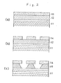
- the exposed resin is dissolved off with an alkaline developer to form an etching resist and these treated material is subjected to an etching with an aqueous acidic solution to dissolve exposed conductive coating, e.g. copper coating.
- exposed conductive coating e.g. copper coating.
- an object of the invention to provide a method for preparing a printed circuit board having fine circuit by using a conventional photosensitive material, with the least change in the processing steps of exposure, development, etching and the like.
- the abovementioned object can be attained with an improvement, in a method for preparing a printed circuit board comprising exposing a photosensitive material which is a laminate of an insulating base plate, an electric conductive coating and a positive working photo resist coating, through a positive mask of circuit pattern placed on said photo resist, to an actinic radiation, developing the photo resist with an aqueous alkaline solution, thereby removing the exposed area and forming an etching resist, subjecting said resist to an etching with an acidic etching solution to remove the exposed conductive coating and finally removing the resist still remained on the unexposed area of the photosensitive material, which is characterized in that after said development and prior to the etching operation, the unexposed resist is further exposed to an actinic radiation.
- any of the conventional positive type photosensitive resin composition may be successfully used, providing that when the formed coating is exposed to an actinic radiation through a circuit pattern, solubility of the exposed resin in a certain solvent is greatly increased as compared with that of the unexposed resin, and only the exposed resin is selectively removed off at the time of development with said solvent.
- Such photo resist coating can be applied on an electric conductive coating by using any of the conventional coating means including an electro-deposition coating, and however, in the case of a printed circuit board having through-holes, particular preference is given to the last mentioned electrodeposition coating. At that time, an electro-depositable, positive type photosensitive resin composition is advantageously used.
- Such resin compositions are an aqueous dispersion of such resin as having a phenolic Novolak resin structure and bearing photosensitive quinone diazide groups and ionic hydrophilic groups as disclosed in Japanese Patent Publication (unexamined) 207139/85; an aqueous dispersion of modified phenol resin having both acidic groups and quinone diazide groups as disclosed in Japanese Patent publication (unexamined) 218616/86; an aqueous dispersion of anionic or cationic acrylic resin containing quinone diazide sulfonic ester as disclosed in Japanese Patent Publication (unexamined) 206293/86; an aqueous dispersion of acrylic resin, polyester resin, epoxy resin or epoxidized polybutadiene resin having, in its side-chains or at the end portions of main chain, imino sulfonate groups as well as salt forming groups as disclosed in Japanese Patent Application No.
- the desired resist pattern may be prepared by using a photosensitive material having such positive working resist coating on a conductive coating (e.g. Cu coating) placed on a printing base plate, exposing such material through a circuit pattern to an actinic radiation and subjection to a development with an alkaline developer.
- a photosensitive material having such positive working resist coating on a conductive coating (e.g. Cu coating) placed on a printing base plate, exposing such material through a circuit pattern to an actinic radiation and subjection to a development with an alkaline developer.
- the positive working photo resist still remained at the unexposed area is subjected to exposure to an actinic radiation, preferably UV rays having wave length of 200 to 500nm, thereby attaining the object of preventing the formation of slender line due to side-etching and obtaining fine circuit pattern.
- an actinic radiation preferably UV rays having wave length of 200 to 500nm
- Japanese Patent Publication (unexamined) 301521/88 is like-wise disclosed a method wherein the resist pattern obtained by development is exposed to UV rays to effect photolysis of photosensitive groups and improve thermal flowability of the resist and thus treated resist is heated to give tapered resist pattern which is suitable for dry etching.
- the resist pattern obtained by development is subjected to deep UV irradiation under heating, thereby effecting exaggerated hardening at the surface area of the resist and forming desired tapered resist pattern. All of the abovementioned techniques concern the formation of tapered resist pattern suitable for dry etching and heat treatment is always required after UV rays exposure (for the control of thermal flowability of the resist).
- such re-flowing step is not required after UV exposure and wet etching is adopted in place of the abovementioned dry etching.
- UV exposure is carried out for the purpose of improving adhesion properties to the base plate and acid resistance of the resist and side-etching at the time of wet etching is effectively controlled therewith. Therefore, the present technique should be strictly distinguished from the abovementioned conventional techniques used in the semiconductor area.
- An electrodeposition bath liquid was prepared by adding a solution of 20 parts of the positive working photosensitive resin obtained in Manufacturing Example 2 in 20 parts of propylene glycol monomethyl ether to 140 parts of the acrylic resin varnish obtained in Manufacturing Example 1, and further combining with 4.6 parts of triethylamine and 815.4 parts of deionized water.
- a printed circuit board base plate composed of an insulating base plate having 0.3mm through-holes previously electrolessly plated and then electroplated with copper in 50 ⁇ m thickness was dipped into the abovementioned electrodeposition bath liquid.
- An electrodeposition bath liquid was prepared by adding 4 parts of triethylamine to 100 parts of the iminosulfonate group bearing acrylic resin obtained in Manufacturing Example 5 and adding 280 parts of deionized water portion to portion, under stirring, to the abovementioned mixture.
- a printed circuit board base plate composed of an insulating base plate having 0.3mm through-holes previously electrolessly plated and then electroplated with copper in 50 ⁇ m thickness was dipped into the abovementioned electrodeposition bath liquid. After connecting the base plate to an anode and the metallic wall of the electrodeposition bath to a cathode, a 50mA/dm2 direct current was impressed at 25°C for 2 minutes and thus treated plate was then washed with water and dried in an air oven maintained at 100°C for 5 minutes to obtain a photosensitive material having a positive working photosensitive resin layer of 7 ⁇ m thickness.
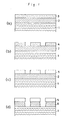
- Fig. 1 shows the cross-section of the photosensitive material used in the invention, each in different stage of the present method (excepting omitting through-holes).
- a positive working photosensitive material (Fig. 1 (a)) obtained in Manufacturing Example 3
- a positive mask having a circuit pattern with 130 ⁇ m width line was placed and the photosensitive material was exposed through said mask to 200 ⁇ 500nm UV rays be using a high pressure mercury lamp.
- exposed material was then developed with an aqueous 1% sodium metasilicate solution to obtain a resist pattern (4) of Fig.1 (b).
- the resist was again exposed to 200 ⁇ 500nm rays by using a high pressure mercury lamp to obtain an exposed resist pattern (5), in which the remained photosensitive groups had been photolytically decomposed to acidic groups, of Fig. 1 (c).
- a wet-etching using a cupric chloride solution was carried out to obtain a circuit pattern (6) with the least side-etching as shown in Fig. 1 (d).
- circuit line had the top width of 110 ⁇ m and the bottom width of 130 ⁇ m.
- Example 2 The similar experiments as stated in Example 1 were repeated by using the photosensitive material obtained in Manufacturing Example 6. However, in this example, development was carried out with an aqueous 2% tetramethylammonium hydroxide solution and at the final stage, the remained resist was removed off by using an aqueous 5% sodium hydroxide solution.
- circuit line had the top width of 105 ⁇ m and the bottom width of 130 ⁇ m.
- circuit line had the top width of 90 ⁇ m and the bottom width of 130 ⁇ m.
- Example 2 Using the photosensitive material as used in Example 2, the same procedures as shown in said Example 2 were repeated, excepting omitting the re-exposure step.
- circuit line had the top width of 85 ⁇ m and the bottom width of 130 ⁇ m.
Landscapes
- Engineering & Computer Science (AREA)
- Manufacturing & Machinery (AREA)
- Microelectronics & Electronic Packaging (AREA)
- Manufacturing Of Printed Circuit Boards (AREA)
- Exposure Of Semiconductors, Excluding Electron Or Ion Beam Exposure (AREA)
Applications Claiming Priority (2)
| Application Number | Priority Date | Filing Date | Title |
|---|---|---|---|
| JP1190068A JPH0353587A (ja) | 1989-07-20 | 1989-07-20 | レジストパターンの形成方法 |
| JP190068/89 | 1989-07-20 |
Publications (2)
| Publication Number | Publication Date |
|---|---|
| EP0409543A2 true EP0409543A2 (de) | 1991-01-23 |
| EP0409543A3 EP0409543A3 (en) | 1992-09-09 |
Family
ID=16251821
Family Applications (1)
| Application Number | Title | Priority Date | Filing Date |
|---|---|---|---|
| EP19900307772 Withdrawn EP0409543A3 (en) | 1989-07-20 | 1990-07-16 | A method for forming a resist pattern |
Country Status (4)
| Country | Link |
|---|---|
| EP (1) | EP0409543A3 (de) |
| JP (1) | JPH0353587A (de) |
| AU (1) | AU633592B2 (de) |
| CA (1) | CA2021536A1 (de) |
Cited By (3)
| Publication number | Priority date | Publication date | Assignee | Title |
|---|---|---|---|---|
| EP0627872A3 (de) * | 1993-05-28 | 1995-03-29 | Ibm | Verfahren zur Herstellung von metallisierten keramischen Substraten. |
| US7875419B2 (en) | 2002-10-29 | 2011-01-25 | Semiconductor Energy Laboratory Co., Ltd. | Method for removing resist pattern and method for manufacturing semiconductor device |
| CN114686884A (zh) * | 2020-12-29 | 2022-07-01 | 苏州运宏电子有限公司 | 一种精密防侧蚀的蚀刻区域控制方法 |
Families Citing this family (1)
| Publication number | Priority date | Publication date | Assignee | Title |
|---|---|---|---|---|
| JP2005209920A (ja) * | 2004-01-23 | 2005-08-04 | Casio Micronics Co Ltd | プリント配線基板、その製造方法および製造装置、配線回路パターン、ならびにプリント配線板 |
Family Cites Families (5)
| Publication number | Priority date | Publication date | Assignee | Title |
|---|---|---|---|---|
| DE2503171A1 (de) * | 1975-01-27 | 1976-07-29 | Siemens Ag | Fotolack-aetzverfahren |
| EP0155231B2 (de) * | 1984-03-07 | 1997-01-15 | Ciba-Geigy Ag | Verfahren zur Herstellung von Abbildungen |
| CA1285418C (en) * | 1985-07-18 | 1991-07-02 | Robert A. Owens | Pre-exposure method for increased sensitivity in high contrast resist development |
| DE3626708A1 (de) * | 1986-08-07 | 1988-02-11 | Mania Gmbh | Verfahren zur herstellung von leiterplatten |
| JPH0740547B2 (ja) * | 1987-03-24 | 1995-05-01 | ウシオ電機株式会社 | レジスト処理方法 |
-
1989
- 1989-07-20 JP JP1190068A patent/JPH0353587A/ja active Pending
-
1990
- 1990-07-16 EP EP19900307772 patent/EP0409543A3/en not_active Withdrawn
- 1990-07-19 AU AU59150/90A patent/AU633592B2/en not_active Ceased
- 1990-07-19 CA CA 2021536 patent/CA2021536A1/en not_active Abandoned
Cited By (4)
| Publication number | Priority date | Publication date | Assignee | Title |
|---|---|---|---|---|
| EP0627872A3 (de) * | 1993-05-28 | 1995-03-29 | Ibm | Verfahren zur Herstellung von metallisierten keramischen Substraten. |
| US7875419B2 (en) | 2002-10-29 | 2011-01-25 | Semiconductor Energy Laboratory Co., Ltd. | Method for removing resist pattern and method for manufacturing semiconductor device |
| CN114686884A (zh) * | 2020-12-29 | 2022-07-01 | 苏州运宏电子有限公司 | 一种精密防侧蚀的蚀刻区域控制方法 |
| CN114686884B (zh) * | 2020-12-29 | 2023-07-07 | 苏州运宏电子有限公司 | 一种精密防侧蚀的蚀刻区域控制方法 |
Also Published As
| Publication number | Publication date |
|---|---|
| AU633592B2 (en) | 1993-02-04 |
| AU5915090A (en) | 1991-01-24 |
| CA2021536A1 (en) | 1991-01-21 |
| JPH0353587A (ja) | 1991-03-07 |
| EP0409543A3 (en) | 1992-09-09 |
Similar Documents
| Publication | Publication Date | Title |
|---|---|---|
| EP0194824B1 (de) | Herstellungsverfahren von Trägern für gedruckte Schaltungen | |
| EP0155231B1 (de) | Verfahren zur Herstellung von Abbildungen | |
| EP0099856B1 (de) | Photopolymerisierbares Beschichtungsmittel, photopolymerisierbares Material und seine Verwendung | |
| CA1298567C (en) | Method for making metallic patterns | |
| EP0204415A2 (de) | Leiterplattenherstellungsverfahren | |
| EP0265387B1 (de) | Bilderzeugungsverfahren | |
| US5055374A (en) | Electrodeposition coating composition containing an acrylic resin and a quinnone diazide group bearing resin | |
| US5314789A (en) | Method of forming a relief image comprising amphoteric compositions | |
| EP0301101B1 (de) | Positive photoempfindliche harzzubereitung | |
| EP0416829B1 (de) | Positiv arbeitende strahlungsempfindliche Harzzusammensetzung | |
| JP2955714B2 (ja) | 導電性パターンの製造方法 | |
| EP0409543A2 (de) | Verfahren zur Ausbildung eines Photoresist-Musters | |
| JPS63271442A (ja) | 画像形成方法 | |
| EP0425437A2 (de) | Verfahren zur Herstellung metallischer Muster | |
| KR100211433B1 (ko) | 포지티브형 음이온 전착 감광성 레지스트 조성물 및 그를 이용한 패턴 형성 방법 | |
| CA1319776C (en) | Process for the production of images | |
| US5166036A (en) | Electrodeposition coating composition and image-forming method using the same | |
| JP2594053B2 (ja) | ポジ型感光性樹脂組成物 | |
| JPS63310196A (ja) | 金属パターンの形成方法 | |
| JP2935207B2 (ja) | ポジ型感光性アニオン電着レジスト組成物およびこの組成物を用いたプリント配線基板の製造方法 | |
| JP2608408B2 (ja) | ポジ型感光性樹脂組成物 | |
| JPS6343393A (ja) | プリント回路板の形成方法 | |
| JPH059791A (ja) | 電着方法 | |
| JPH0675370A (ja) | ポジ型感光性カチオン電着レジスト組成物およびこの組成物を用いたプリント配線基板の製造方法 |
Legal Events
| Date | Code | Title | Description |
|---|---|---|---|
| PUAI | Public reference made under article 153(3) epc to a published international application that has entered the european phase |
Free format text: ORIGINAL CODE: 0009012 |
|
| AK | Designated contracting states |
Kind code of ref document: A2 Designated state(s): DE FR GB NL |
|
| PUAL | Search report despatched |
Free format text: ORIGINAL CODE: 0009013 |
|
| AK | Designated contracting states |
Kind code of ref document: A3 Designated state(s): DE FR GB NL |
|
| 17P | Request for examination filed |
Effective date: 19930226 |
|
| 17Q | First examination report despatched |
Effective date: 19931230 |
|
| STAA | Information on the status of an ep patent application or granted ep patent |
Free format text: STATUS: THE APPLICATION IS DEEMED TO BE WITHDRAWN |
|
| 18D | Application deemed to be withdrawn |
Effective date: 19940712 |