EP0410307B1 - Dispositif électroluminescent et sa méthode de fabrication - Google Patents
Dispositif électroluminescent et sa méthode de fabrication Download PDFInfo
- Publication number
- EP0410307B1 EP0410307B1 EP90113874A EP90113874A EP0410307B1 EP 0410307 B1 EP0410307 B1 EP 0410307B1 EP 90113874 A EP90113874 A EP 90113874A EP 90113874 A EP90113874 A EP 90113874A EP 0410307 B1 EP0410307 B1 EP 0410307B1
- Authority
- EP
- European Patent Office
- Prior art keywords
- substrate
- clad
- layer
- light
- layers
- Prior art date
- Legal status (The legal status is an assumption and is not a legal conclusion. Google has not performed a legal analysis and makes no representation as to the accuracy of the status listed.)
- Expired - Lifetime
Links
Images



Classifications
-
- H—ELECTRICITY
- H10—SEMICONDUCTOR DEVICES; ELECTRIC SOLID-STATE DEVICES NOT OTHERWISE PROVIDED FOR
- H10H—INORGANIC LIGHT-EMITTING SEMICONDUCTOR DEVICES HAVING POTENTIAL BARRIERS
- H10H20/00—Individual inorganic light-emitting semiconductor devices having potential barriers, e.g. light-emitting diodes [LED]
- H10H20/80—Constructional details
- H10H20/81—Bodies
- H10H20/819—Bodies characterised by their shape, e.g. curved or truncated substrates
- H10H20/821—Bodies characterised by their shape, e.g. curved or truncated substrates of the light-emitting regions, e.g. non-planar junctions
-
- H—ELECTRICITY
- H10—SEMICONDUCTOR DEVICES; ELECTRIC SOLID-STATE DEVICES NOT OTHERWISE PROVIDED FOR
- H10H—INORGANIC LIGHT-EMITTING SEMICONDUCTOR DEVICES HAVING POTENTIAL BARRIERS
- H10H20/00—Individual inorganic light-emitting semiconductor devices having potential barriers, e.g. light-emitting diodes [LED]
- H10H20/01—Manufacture or treatment
- H10H20/011—Manufacture or treatment of bodies, e.g. forming semiconductor layers
- H10H20/013—Manufacture or treatment of bodies, e.g. forming semiconductor layers having light-emitting regions comprising only Group III-V materials
-
- H—ELECTRICITY
- H10—SEMICONDUCTOR DEVICES; ELECTRIC SOLID-STATE DEVICES NOT OTHERWISE PROVIDED FOR
- H10W—GENERIC PACKAGES, INTERCONNECTIONS, CONNECTORS OR OTHER CONSTRUCTIONAL DETAILS OF DEVICES COVERED BY CLASS H10
- H10W72/00—Interconnections or connectors in packages
- H10W72/50—Bond wires
- H10W72/531—Shapes of wire connectors
- H10W72/5363—Shapes of wire connectors the connected ends being wedge-shaped
-
- H—ELECTRICITY
- H10—SEMICONDUCTOR DEVICES; ELECTRIC SOLID-STATE DEVICES NOT OTHERWISE PROVIDED FOR
- H10W—GENERIC PACKAGES, INTERCONNECTIONS, CONNECTORS OR OTHER CONSTRUCTIONAL DETAILS OF DEVICES COVERED BY CLASS H10
- H10W72/00—Interconnections or connectors in packages
- H10W72/50—Bond wires
- H10W72/59—Bond pads specially adapted therefor
-
- H—ELECTRICITY
- H10—SEMICONDUCTOR DEVICES; ELECTRIC SOLID-STATE DEVICES NOT OTHERWISE PROVIDED FOR
- H10W—GENERIC PACKAGES, INTERCONNECTIONS, CONNECTORS OR OTHER CONSTRUCTIONAL DETAILS OF DEVICES COVERED BY CLASS H10
- H10W72/00—Interconnections or connectors in packages
- H10W72/90—Bond pads, in general
- H10W72/931—Shapes of bond pads
- H10W72/932—Plan-view shape, i.e. in top view
Definitions
- the present invention relates to a light-emitting device such as a semiconductor laser or a light-emitting diode adapted for use in optical communication system, optical integrated circuit, display or the like, and a method for producing said device.
- a light-emitting device such as a semiconductor laser or a light-emitting diode adapted for use in optical communication system, optical integrated circuit, display or the like, and a method for producing said device.
- wavelength-multiplex optical communication For high-speed transmission or information of a large amount, there is already known wavelength-multiplex optical communication.
- the transmission of information is achieved by simultaneously passing, in an optical fiber, plural light beams of mutually different wavelengths, containing mutually independent signals.
- the light source employed in such optical communication is so constructed as to synthesize light beams, emitted from plural separate semiconductor lasers, in an optical synthesizer and to guide thus synthesized light beams into the optical fiber.
- Such optical synthesizer is described for example by Kojima et al., FPO, Vo.l, 4, No. 7, p. 45 (1979).
- the object of the present invention is to provide a light-emitting device containing plural light-emitting elements integrated with a high density, and an inexpensive and simple method for producing the same.
- a light-emitting device comprising: a substrate; a first clad layer formed on a part of said substrate; a first active layer formed on the outer periphery of said first clad layer on said substrate and adapted to emit light by current injection; a second clad layer formed on the outer periphery of said first active layer on the substrate, wherein said first active layer and first and second clad layers constitute a first double heterogeneous structure having junctions substantially perpendicular to the surface of the substrate; a second active layer formed on the outer periphery of said second clad layer on the substrate and adapted to emit light by current injection; a third clad layer fomred on the outer periphery of said second active layer on the substrate, wherein said second active layer and second and third clad layers constitute a second double heterogeneous structure having junctions substantially perpendicular to the surface of the substrate; and electrodes for current supply to said first and
- a method for producing the above-mentioned light-emitting device comprising steps of: forming, on a part of the surface of a substrate, a nucleation area of a higher nucleation density than in other areas and of a sufficiently small area so as to allow single crystal growth thereon only from a single nucleus; forming, on said nucleation area, a first clad layer consisting of monocrystalline semiconductor; forming a first active layer consisting of monocrystalline semiconductor on the outer periphery of said first clad layer on the substrate; forming a second clad layer consisting of monocrystalline semiconductor on the outer periphery of said first active layer on the substrate, whereby said first active layer and first and second clad layers constitute a first double heterogeneous structure; forming a second active layer consisting of monocrystalline semiconductor on the outer periphery of said second clad layer on the substrate; forming a third clad layer on the outer periphery of said second active layer
- Figs. 2A and 1B are respectively a schematic plan view and a schematic cross-sectional view of a first embodiment of the light-emitting device of the present invention.
- a first clad layer 3a consisting of mono-crystalline semiconductor.
- a first active layer 4a there are concentrically formed, in succession, a first active layer 4a, a second clad layer 3b, a second active layer 4b and a third clad layer 3c.
- electrodes 5a, 5b, 5c there are respectively formed electrodes 5a, 5b, 5c, which are connected to an unrepresented external power source respectively through lead wires 6a, 6b, 6c.
- the conductive type of said first and third clad layers 3a, 3c is different from that of the second clad layer 3b.
- the semiconductor material constituting the first active layer 4a is different, in combination and/or composition of elements, from that constituting the first and second clad layers 3a, 3b. Consequently these layers constitute a first double heterogeneous structure having junction planes substantially perpendicular to the surface of the substrate.
- the second active layer 4b and the second and third clad layers 3b, 3c are composed of mutually different semiconductor materials, and constitute a second double heterogeneous structure having junction planes substantially perpendicular to the surface of the substrate.
- first and second light emissions can be independently controlled by the adjustment of the injected currents.
- the first and second lights can be of a same wavelength, or can be of different wavelengths by employing different materials or compositions in the active layers.
- the present invention realizes a compact structure of the light-emitting device emitting plural light beams, as independently controllable light-emitting elements can be positioned very closely. Also as the light-emitting areas in the light-emitting device of the present invention are positioned parallel to the surface of the substrate, there can be obtained a light source providing a larger number of light beams by forming plural devices on a same substrate. It is furthermore possible to form a plurality of the light-emitting devices of the present invention, in a two-dimensional arrangement, on a same substrate.
- the device of the present invention can be prepared by a method of growing a single-crystal on an amorphous or polycrystalline substrate, utilizing the difference in nucleation density (hereinafter called selective nucleation method).
- selective nucleation method is disclosed for example in the Europena Laid-Open Patent No. 244,081.
- the European Laid-Open Patent No. 285,358 discloses the technology for producing a light-emitting diode, utilizing said selection nucleation method. In the following there will be explained the method for producing the light-emitting device of the present invention, utilizing the selective nucleation method.
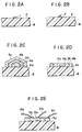
- Figs. 2A to 2E are schematic cross-sectional views showing the method for producing the device of the above-explained first embodiment, wherein said components as those in Fig. 1B are represented by same numbers and will not be explained further.
- the surface of the amorphous substrate 8 is a non-nucleation surface with a low nucleation density.
- a small deposition film 1 with a nucleation surface having a higher nucleation density than in said non-nucleation surface is formed, as shown in Fig. 2A.
- the size of said nucleation surface is made sufficiently small so that crystal growth thereon takes place only from a single nucleus.
- a monocrystalline grain 7 consisting of a III-V semi-conductive compound such as GaAs, AlGaAs, InP, GaInAlAs or GaInP for example by metal organic chemical vapor deposition (MOCVD), liquid phase epitaxy (LPE) or gas source molecular beam epitaxy (gas source MBE). Because of the difference in the nucleation density, said monocrystalline grain 7 grows on the deposition film 1 as shown in Fig. 2B. Because the size of the nucleation surface of the deposition film 1 is very small, the grain 7 grows from a single nucleus and becomes a single crystal.
- MOCVD metal organic chemical vapor deposition
- LPE liquid phase epitaxy
- gas source MBE gas source molecular beam epitaxy
- first clad layer 3a first active layer 4a, second clad layer 3b, second active layer 4b and third clad layer 3c are made in succession around the monocrystalline grain 7 explained above.
- These clad layers and active layers are formed with desired characteristics, for example conductive type, by the adjustments of semiconductor material, composition thereof, and doping impurity therefor.
- the surface of thus grown semiconductive layers is made planar, parallel to the surface of the substrate, whereby the clad layers and active layers 3a, 4a, 3b, 4b are exposed.
- Electrodes 5a, 5b, 5c as shown in Fig. 2E, and lead wires 6a, 6b, 6c are respectively bonded to said electrodes 5a, 5b, 5c.
- the light-emitting device of the first embodiment is thus completed.
- the following there will be explained a more specific example.
- the present example providing a semiconductive laser having two active layers composed of i-GaAs and i-Ga 0.9 Al 0.1 As, has a structure same as that of the first embodiment and was prepared by a process shown in Figs. 2A to 2E.
- Al2O3 was deposited by evaporation on an amorphous SiO2 substrate 8 and was etched off, leaving a small area (1.2 ⁇ m square), whereby a non-nucleation surface (SiO2) 2 and a deposition film 1 constituting the nucleation surface (Al2O3) were formed as shown in Fig. 2A.
- a monocrystalline grain 7 consisting of h-Ga 0.75 Al 0.25 As was formed as shown in Fig. 2B by MOCVD at a growth temperature 600 °C, employing H2 as carrier gas at a rate of 3 l/min., t-butyl arsine (TEAs) at 3 x 10 ⁇ 4 mol/min., trimethyl gallium (TMG) at 3 x 10 ⁇ 5 mol/min. and trimethyl aluminum (TMAl) at 1 x 10 ⁇ 5 mol/min. as source materials, and diethyl zinc (DEZn) as the doping material.
- H2 carrier gas
- TEAs t-butyl arsine
- TMG trimethyl gallium
- TMAl trimethyl aluminum
- DEZn diethyl zinc
- the surface of the grown crystal was planarized by reactive ion beam etching (RIBE) as shown in Fig. 2D, thereby exposing the p-Ga 0.75 -Al 0.25 As clad layer 3a, n-Ga 0.75 Al 0.25 As clad layer 3b and p-Ga 0.75 Al 0.25 As clad layer 3c.
- RIBE reactive ion beam etching
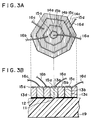
- Figs. 3A and 3B are respectively a schematic plan view and a schematic cross-sectional view of a second embodiment of the light-emitting device of the present invention.
- Said second embodiment is prepared by the selective nucleation method as in the first embodiment, but is different therefrom in the method of forming the nucleation surface.
- a substrate 19 composed for example of Al2O3
- a layer composed for example of SiO2 and constituting a non-nucleation surface 12.
- a nucleation surface 11 by impurity ion implantation.
- first clad layer 13a consisting of monocrystalline semiconductor.
- first active layer 14a a first active layer 14a
- second clad layer 13b a second active layer 14b
- third clad layer 13c a third active layer 14c
- fourth clad layer 13d On said clad layers 13a, 13b, 13c and 13d, there are respectively formed electrodes 15a, 15b, 15c and 15d, which are connected to an unrepresented external power source through lead wires 16a, 16b, 16c and 16d.
- the conductive type of said clad layers 13a and 13c is different from that of the clad layers 13b and 13d.
- the active layer 14a and the clad layers 13a, 13b are composed of semiconductive materials which are mutually different in combination and/or composition of elements, and therefore constitute a first double heterogeneous structure having junction planes substantially perpendicular to the surface of the substrate.
- the active layer 14b and the clad layers 13b, 13c constitute a second double heterogeneous structure
- the active layer 14c and the clad layers 13c, 13d constitute a third double heterogeneous structure.
- an electric current is injected into the first active layer 14a, said active layer emits first light above and below perpendicularly to the surface of the substrate.
- current injections into the active layers 14b, 14c causes second and third light emissions perpendicular to the surface of the substrate.
- Said first to third light emissions can be independently controlled by the adjustment of the injected currents.
- Said first to third lights can be of a same wavelength, or can be different wavelengths of employing different materials or compositions in said active layers.
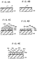
- Figs. 4A to 4E are schematic cross-sectional views showing the method for producing the device of the above-explained second embodiment, wherein same components are those in Fig. 3B are represented by same numbers and will not be explained further.
- a non-nucleation surface 12 of a low nucleation density On the surface of the substrate 19, there is formed a non-nucleation surface 12 of a low nucleation density. In a part of said surface 12 there is formed a nucleation surface 11 by implantation of an impurity such as As ions. The size of said nucleation surface is made sufficiently small so that crystal growth thereon takes place only from a single nucleus.
- a monocrystalline grain 7 consisting of a III-V compound semiconductor as in the 1st embodiment. Because of the difference in nucleation density, the monocrystalline grain 17 grows on the nucleation surface 11 as shown in Fig. 4B. Because the size of the nucleation surface 11 is very small, the grain 7 grows from a single nucleus and becomes a single crystal.
- clad layer 13a there are conducted monocrystalline growths in succession of the clad layer 13a, active layer 14a, clad layer 13b, active layer 14b, clad layer 13c, active layer 14c and clad layer 13d.
- These clad layers and active layers are formed with desired characteristics, for example conductive type, by the adjustments of semiconductor material, composition thereof and doping impurity therefor.
- the surface of thus grown semiconductive layers is planarized parallel to the surface of the substrate, whereby the clad layers 13a, 13b, 13c and active layers 14a, 14b, 14c are exposed.
- Electrodes 15a, 15b, 15c as shown in Fig. 4C, and lead wires 16a, 16b, 16c are bonded to said electrodes.
- the light-emitting device of the second embodiment is thus completed.
- the following there will be explained a more specific example.
- the present example providing a light-emitting diode device having three active layers consisting of i-GaAs, i-Ga 0.95 Al 0.05 As and i-Ga 0.9 Al 0.1 As, has a same structure as that of the second embodiment and was prepared by a process shown in Figs. 4A to 4E.
- SiO2 was deposited by evaporation to form the non-nucleation surface 12 on a ceramic substrate 19. Then As ions were implanted in a small area (size about 1.2 ⁇ m) square to form the nucleation surface 11 of a higher nucleation density.
- a n-Ga 0.8 Al 0.2 As clad layer 13a an i-GaAs active layer 14a, a p-Ga 0.8 -Al 0.2 As clad layer 13d, an i-Ga 0.95 Al 0.05 As active layer 14b, a n-Ga 0.8 Al 0.2 As clad layer 13c, an i-Ga 0.9 Al 0.1 As active layer 14c, and a p-Ga 0.8 Al 0.2 As clad layer 13d as shown in Fig.
- n-Ga 0.8 Al 0.2 As clad layer 13a n-Ga 0.8 Al 0.2 As clad layer 13a
- p-Ga 0.8 Al 0.2 As clad layer 13b n-Ga 0.8 Al 0.2 As clad layer 13c and Ga 0.8 Al 0.2 As clad layer 13d.
- conductive electrode layers 15a - 15d were formed, and lead wires 16a - 16d were respectively bonded to said electrodes. The light-emitting diode device was thus completed.
- the lead wires 16a, 16b were grounded and the lead wires 16b, 16d were given a current of 100 mA in pulse operation at room temperature, whereby the i-GaAs active layer 14a, i-Ga 0.95 Al 0.05 As active layer 14b and i-Ga 0.9 Al 0.1 -As active layer 14c respectively emitted lights of wavelengths of ⁇ - 0.9, 0.87 and 0.85 ⁇ m.
- Said LED device had a size of 44 x 44 ⁇ m and was easy to prepare.
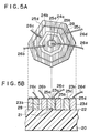
- Figs. 5A and 5B are respectively a schematic plan view and a schematic cross-sectional view of a third embodiment of the light-emitting device of the present invention.
- the third embodiment is prepared by the selective nucleation method as in the first embodiment.
- a substrate 20 consisting of an amorphous material such as SiO2 or Al2O3 has a non-nucleation surface 22 of a low nucleation density.
- a nucleation surface 21 is formed by depositing a film on a part of said non-nucleation surface 22.
- first clad layer 23a consisting of monocrystalline semiconductor.
- first active layer 24a a first active layer 24a
- second clad layer 23b a high resistance layer 28
- third clad layer 23c a second active layer 24b
- fourth clad layer 25c a fourth clad layer 25c.
- electrodes 25a, 25b, 25c and 25d are respectively formed on said clad layers 23a, 23b, 23c and 23d, which are connected to an unrepresented external power source through lead wires 26a, 26b, 26c and 26d.
- the clad layers 23a and 23b having mutually different conductive types. Also the clad layers 23c and 23d have mutually different conductive types. Furthermore, the active layer 24a and the clad layers 23a, 23b are composed of semiconductor materials which mutually different in combination and/or composition of elements, and constitute, therefore, a first double heterogeneous structure having junction planes substantially perpendicular to the surface of the substrate. Similarly the active layer 24b and the clad layers 23c, 23d constitute a second double heterogeneous structure.
- a current injection into the active layer 24a through the electrodes 25a, 25b causes first light emission from said active layer 24a above and below perpendicularly to the surface of the substrate.
- a current injection into the active layer 24b through the electrodes 25c, 25d causes second light emission perpendicular to the surface of the substrate.
- Said first and second light emission can be independently controlled by the adjustment of injected currents.
- Said first and second lights can be of a same wavelength, or of mutually different wavelengths, by employing different materials and/or compositions in said active layers.
- the high resistance layer 28 electrically separates the clad layers 23b and 23c, thereby preventing eventual current lead between said first and second double heterogeneous structures.
- This structure provides an advantage of enabling light emission of higher efficiency and lower noises.
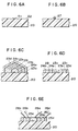
- Figs. 6A to 6E are schematic cross-sectional views showing the process for producing the device of the third embodiment, wherein same components as those in Fig. 5B are represented by same numbers and will not be explained further.
- the surface of a substrate 20 constitutes a non-nucleation surface 22.
- a nucleation surface 21 is formed by providing a part of said surface 22 with a deposition film as shown in Fig. 6A. The size of said nucleation surface is made sufficiently small so that the crystal growth thereon takes place only from a single nucleus.
- a monocrystalline grain 27 consisting of a III-V compound semiconductor as in the 1st embodiment, for example by MOCVD, LPE or gas source MBE.
- Said crystal growth is conducted with materials such as trimethyl gallium (TMG), t-butyl arsine (TBAs), As H3 etc.
- TMG trimethyl gallium
- TAAs t-butyl arsine
- As H3 etc.
- the growth temperature is generally in a range of 500 - 800 °C, preferably 570 - 760 °C, most preferably 600 - 700 °C.
- the pressure at crystal growth is generally in a range of 1 - 80 Torr, preferably 1 - 30 Torr, and most preferably 1 - 10 Torr.
- the monocrystalline grain 27 grows on the nucleation surface 21 as shown in Fig. 6B. Because the size of the nucleation surface 21 is very small, the grain 27 grows from a single nucleus and becomes a single crystal.
- a clad layer 23a, an active layer 24a, a clad layer 23b, a high resistance layer 28, a clad layer 23c, an active layer 24b and a clad layer 23d as shown in Fig. 6C, by changing the pressure generally in a range of 50 - 760 Torr, preferably 100 - 760 Torr and most preferably 300 - 760 Torr, increasing the amount of raw materials and adding an aluminum source such as trimethyl aluminum (TMAl).
- TMAl trimethyl aluminum
- the surface of the grown semiconductor layers is planarized parallel to the surface of the substrate, whereby the clad layers 23a, 23b, 23c, high resistance layer 28 and active layers 24a, 24b are exposed.
- Electrodes 25a, 25b, 25c, 25d as shown in Fig. 6E, and lead wires 26a, 26b, 26c, 26d are respectively bonded.
- the light-emitting device of the 3rd embodiment is prepared in this manner. In the following there will be explained a more specific example.
- the present example providing a semiconductor laser device having two active layers consisting of i-GaAs and i-Ga 0.9 Al 0.1 As, has a same structure as in the 3rd embodiment, and was prepared by the process shown in Figs. 6A to 6E.
- Al2O3 was deposited by evaporation on a amorphous SiO2 substrate 20 and was etched off, leaving a small area (1.2 ⁇ m square), whereby a non-nucleation surface (SiO2) 22 and a nucleation surface (Al2O3) 21 were formed as shown in Fig. 6A.
- a monocrystalline grain 27 consisting of p-Ga 0.75 Al 0.25 As was formed as shown in Fig. 6B by MOCVD at a growth temperature of 600 °C, employing H2 as carrier gas at a rate of 3 l/min., t-butyl arsine (TEAs) at 3 x 10 ⁇ 4 mol/min., trimethyl gallium (TMG) at 3 x 10 ⁇ 5 mol/min. and trimethyl aluminum (TMAl) at 1 x 10 ⁇ 5 mol/min. as source materials, and diethyl zinc (DEZn) as the doping material.
- H2 carrier gas
- TEAs t-butyl arsine
- TMG trimethyl gallium
- TMAl trimethyl aluminum
- DEZn diethyl zinc
- a p-Ga 0.75 Al 0.25 As clad layer 23a an i-GaAs active layer 24a, a n-Ga 0.75 -Al 0.25 As clad layer 23b, an i-Ga 0.7 Al 0.3 As high resistance layer 28, a n-Ga 0.75 Al 0.25 As clad layer 23c, an i-Ga 0.9 Al 0.1 As active layer 24b and a p-Ga 0.75 Al 0.25 As clad layer 23d as shown in Fig.
- the surface of the grown crystal was planarized by RIBE as shown in Fig. 6E to expose the clad layers 23a - 23c.
- conductive electrode layers 25a - 25d As shown in Fig. 6E, on thus exposed surfaces, there were formed conductive electrode layers 25a - 25d, and Au lead wires 26a - 26d were respectively bonded thereto.
- the i-GaAs active layer 24a shown a threshold current of 200 mA, while the i-Ga 0.9 Al 0.1 As active layer 24b showed a threshold current of 410 mA.
- Figs. 7A and 7B are respectively a schematic plan view and a schematic cross-sectional view of a fourth embodiment of the light-emitting device of the present invention.
- Said fourth embodiment is prepared by the selective nucleation method as in the third embodiment, but is different therefrom in the method of forming the nucleation surface.
- a substrate 39 composed for example of Al2O3
- a layer composed for example of SiO2 and constituting a non-nucleation surface 32.
- an nucleation surface 31 by impurity ion implantation.
- first clad layer 33a consisting of monocrystalline semiconductor.
- first active layer 34a On said nucleation surface 31 there is formed a first clad layer 33a consisting of monocrystalline semiconductor.
- first clad layer 33a Around said first clad layer 33a, there are formed in succession, in concentric manner, a first active layer 34a, a second clad layer 33b, a first high resistance layer 38a, a third clad layer 33c, a second active layer 34b, a fourth clad layer 33d, a second high resistance layer 38b, a fifth clad layer 33e, a third active layer 34c and a sixth clad layer 33f.
- Electrodes 35a, 35b, 35c, 35d, 35e and 35f there are respectively formed electrodes 35a, 35b, 35c, 35d, 35e and 35f, which are connected to an unrepresented external power source through lead wires 36a, 36b, 36c, 36d, 36e and 36f.
- Said clad layer pair 33a and 33b; 33c and 33d; or 33e and 33f have mutually different conductive types.
- the active layer 34a and the clad layers 33a, 33b are composed of semiconductive materials which are mutually different in combination and/or composition of elements, and therefore constitute a first double heterogeneous structure having junction planes substantially perpendicular to the surface of the substrate.
- the active layer 34b and the clad layers 33c, 33d constitute a second double heterogeneous structure
- the active layer 34c and the clad layers 33e, 33f constitute a third double heterogeneous structure.
- a current injection into the active layer 34a induces first light emission above and below perpendicular to the surface of the substrate.
- current injections to the active layers 34b, 34c induce second and third light emissions perpendicular to the surface of the substarte.
- These first to third light emissions can be independently controlled by the adjustment of the injected currents.
- Said first to third lights can be of a same wavelength, or can be of mutually different wavelengths by employing different materials or compositions in said active layers.
- the high resistance layer 38a electrically separates the clad layers 33b and 33c, while the high resistance layer 38b electrically separates the clad layers 33d and 33e.
- these high resistance layers prevent mutual current leakage among the 1st to 3rd double heterogeneous structures.
- the structure of the present embodiment provides an advantage of light emission of higher efficiency and lower noises.
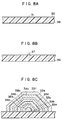
- Figs. 8A to 8E are schematic cross-sectional views showing the process for producing the device of the 4th embodiment, wherein same components as those in Fig. 7B are represented by same numbers and will not be explained further.
- the surface of a substrate 39 constitutes a non-nucleation surface 32.
- a nucleation surface 31 by impurity ion implantation.
- the size of said nucleation surface is made sufficiently small so that the crystal growth thereon takes place only from a single nucleus.
- a monocrystalline grain 37 consisting of a III-V compound semiconductor as in the 3rd embodiment, for example by MOCVD, LPE or gas source MBE. Said crystal growth is conducted with same materials, growth temperature and pressure in the film forming apparatus as those in the 3rd embodiment. Because of the difference in nucleation density, the monocrystalline grain 37 grows on the nucleation surface 31 as shown in Fig. 8B. Because the size of the nucleation surface 31 is very small, the grain 37 grows from a single nucleus and becomes a single crystal.
- a clad layer 33a an active layer 34a, a clad layer 33b, a high resistance layer 38a, a clad layer 33c, an active layer 34b, a clad layer 33d, a high resistance layer 38b, a clad layer 33e, an active layer 34c and a clad layer 33f, as shown in Fig. 8C by changing the pressure as in the 3rd embodiment, increasing the amount of supplied raw materials and adding aluminum-containing material thereto.
- These clad layers and active layers are formed with desired characteristics, for example conductive type, by the adjustment of the semiconductor materials, composition thereof, and doping material.
- the surface of the grown semiconductors layers is planarized parallel to the surface of the substrate, whereby the clad layers 33a, 33b, 33c, 33d, 33e are exposed.
- Electrodes 35a - 35f as shown in Fig. 8E, and lead wires 36a - 36g are respectively bonded.
- the light-emitting device of the 4th embodiment is prepared in this manner. In the following there will be explained a more specific example.
- the present example providing a light-emitting diode device having three active layers respectively of i-GaAs, i-Ga 0.95 Al 0.05 As and i-Ga 0.9 Al 0.1 As, has a same structure as in the 4th embodiment and was prepared by the process shown in Figs. 8A - 8E.
- SiO2 was deposited by evaporation to form a non-nucleation surface 32 on a ceramic substrate 39. Then As ions were implanted in a small area (size about 1.2 ⁇ m square) to form the nucleation surface 31 of a higher nucleation density.
- a n-Ga 0.8 Al 0.2 As clad layer 33a an i-GaAs active layer 34a, a p-Ga 0.8 Al 0.2 As clad layer 33b, an i-Ga 0.7 Al 0.3 As high resistance layer 38a, a p-Ga 0.8 Al 0.2 As clad layer 38c, an i-Ga 0.95 Al 0.05 As active layer 34b, a n-Ga 0.8 Al 0.2 As clad layer 33d, an i-Ga 0.7 Al 0.3 As clad layer 33d, an i-Ga 0.7 Al 0.3 As high resistance layer 38b, a p-Ga 0.8 Al 0.2 As clad layer 33e, an i-Ga 0.9 Al 0.1 As active layer 34c and a n-Ga 0.8 Al 0.2 As clad layer 33f as shown in Fig.
- conductive electrode layers 35a - 35f were formed as shown in Fig. 8E, and lead wires 36a -36f were respectively bonded.
- the present invention is applicable to various purposes.
- the high resistance layers in the 3rd and 4th embodiments may be replaced by insulating layers.
- the light-emitting device of the present invention is usable not only to the light source of the aforementioned optical communication system but also to other various applications.
- a color display without color filters can be obtained by arranging the light-emitting devices of the present invention, having three active layers respectively emitting red, blue and green lights, two-dimensionally on a same substrate.
- a light-emitting device having a first clad layer on a substrate, and a first active layer for light emission by current injection, a second clad layer constituting a first heterogeneous structure with the first active layer and first clad layer, a second active layer for light emission by current injection, a third clad layer constituting a second heterogeneous structure with the second active layer and second clad layer, all formed in concentric manner around the first clad layer, and an electrode for supplying the first and second active layers with electric currents, thereby emitting lights from the first and second active layers by current injection.
Landscapes
- Led Devices (AREA)
Claims (35)
- Dispositif électroluminescent comportant :
un substrat (8) ;
une première couche (3a) de revêtement formée sur une partie dudit substrat ;
une première couche active (4a) formée sur la périphérie extérieure de ladite première couche (3a) de revêtement sur le substrat (8) et destinée à émettre de la lumière par une injection de courant ;
une deuxième couche de revêtement (3b) formée sur la périphérie extérieure de ladite première couche active (4a) sur le substrat, ladite première couche active (4a) et lesdites Première (3a) et deuxième (3b) couches de revêtement constituant une première structure hétérogène double ayant des plans de jonction sensiblement perpendiculaires à la surface du substrat (8) ;
une deuxième couche active (4b) formée sur la périphérie extérieure de ladite deuxième couche (3b) de revêtement sur le substrat et destinée à émettre de la lumière par une injection de courant ;
une troisième couche (3c) de revêtement formée sur la périphérie extérieure de ladite deuxième couche active (4b) sur le substrat, ladite deuxième couche active (4b) et lesdites deuxième (3b) et troisième (3c) couches de revêtement constituant une seconde structure hétérogène double ayant des plans de jonction sensiblement perpendiculaires à la surface du substrat ; et
des électrodes (5a, 5b, 5c) destinées à alimenter lesdites première et deuxième couches actives en courants électriques. - Dispositif électroluminescent selon la revendication 1, dans lequel lesdites première et deuxième couches actives émettent des lumières ayant des longueurs d'ondes mutuellement différentes.
- Dispositif électroluminescent selon la revendication 1, dans lequel lesdites première et troisième couches de revêtement ont l'un des types p et n de conduction, et ladite deuxième couche de revêtement a l'autre type de conduction.
- Dispositif électroluminescent selon la revendication 3, dans lequel lesdites couches actives sont composées de semiconducteurs non dopés.
- Dispositif électroluminescent selon la revendication 1, dans lequel lesdites couches actives et lesdites couches de revêtement sont composées de semiconducteurs composés faisant partie des Groupes III-V du Tableau Périodique.
- Dispositif électroluminescent selon la revendication 5, dans lequel ladite couche active et lesdites couches de revêtement sont composées de GaAs et de GaAlAs.
- Dispositif électroluminescent selon les revendications 1-6, dans lequel ledit substrat présente une surface de formation de cristaux constituée d'une surface (12) de non-nucléation à faible densité de nucléation et d'une surface (11) de nucléation ayant une densité de nucléation plus élevée que celle de ladite surface de non-nucléation, positionnée de façon à être adjacente à ladite surface de non-nucléation et ayant une dimension suffisamment petite pour que la croissance de cristaux sur elle ait lieu uniquement à partir d'un noyau unique ;
ladite première couche de revêtement étant formée sur une petite étendue sur la surface de nucléation dudit substrat ;
lesdites première, deuxième et troisième couches de revêtement et lesdites première et deuxième couches actives étant constituées d'un semiconducteur monocristallin. - Dispositif électroluminescent selon la revendication 7, dans lequel ledit substrat est composé d'un élément à faible densité de nucléation et d'un film composé d'une matière à densité de nucléation plus élevée que celle dudit élément et formé dans une partie de la surface dudit élément.
- Dispositif électroluminescent selon la revendication 8, dans lequel ledit substrat est composé d'un élément à plaque constitué de SiO₂ et d'un petit film constitué d'Al₂O₃ formé sur la surface dudit élément à plaque.
- Dispositif électroluminescent selon la revendication 7, dans lequel ledit substrat est composé d'un élément à faible densité de nucléation et d'une surface de nucléation formée dans une partie de la surface dudit élément par implantation d'ions d'une impureté.
- Dispositif électroluminescent selon la revendication 10, dans lequel ledit substrat est composé d'un élément à plaque céramique, d'un film de SiO₂ formé sur lui et d'ions As implantés dans une petite étendue sur la surface dudit film.
- Procédé pour produire un dispositif électroluminescent, comprenant les étapes qui consistent :
à former, dans une partie de la surface d'un substrat (8), une surface (11) de nucléation ayant une densité de nucléation supérieure à celle d'une autre partie et d'une dimension suffisamment petite pour qu'une croissance cristalline ait lieu sur elle seulement à partir d'un noyau unique ;
à former, sur ladite surface de nucléation, une première couche (3a) de revêtement constituée d'un semiconducteur monocristallin ;
à former, sur la périphérie extérieure de ladite première couche de revêtement sur le substrat, une première couche active (4a) constituée d'un semiconducteur monocristallin ;
à former, sur la périphérie extérieure de ladite première couche active sur le substrat, une deuxième couche (3b) de revêtement constituée d'un semiconducteur monocristallin, ladite première couche active (4a) et lesdites première (3a) et deuxième (3b) couches de revêtement constituant une première structure hétérogène double ;
à former, sur la périphérie extérieure de ladite deuxième couche (3b) de revêtement sur le substrat, une deuxième couche active (4b) constituée d'un semiconducteur monocristallin ;
à former, sur la périphérie extérieure de ladite deuxième couche active sur le substrat, une troisième couche (3c) de revêtement, ladite deuxième couche active (4b) et lesdites deuxième et troisième couches de revêtement constituant une seconde structure hétérogène double ; et
à former des électrodes (5a, 5b, 5c) pour alimenter lesdites première et deuxième couches actives en courants électriques. - Procédé selon la revendication 12, dans lequel ladite surface de nucléation est formée par formation, dans une partie de la surface d'un élément à faible densité de nucléation, d'un petit film d'une matière ayant une densité de nucléation supérieure à celle dudit élément.
- Procédé selon la revendication 12, dans lequel ladite surface de nucléation est formée par implantation d'ions d'une impureté dans une partie de la surface d'un élément à faible densité de nucléation.
- Procédé selon la revendication 12, dans lequel lesdites couches actives et lesdites couches de revêtement sont formées par dépôt chimique en phase vapeur aux organo-métalliques (MOCVD) par épitaxie en phase liquide (LPE) ou par épitaxie par faisceau moléculaire à source de gaz (MBE à source de gaz).
- Procédé selon la revendication 12, comprenant en outre une étape consistant à aplanir les couches actives et les couches de revêtement formées sur le substrat, avant la formation desdites électrodes.
- Procédé selon la revendication 16, dans lequel l'étape d'aplanissement est conduite par gravure par faisceau ionique réactif (RIBE).
- Dispositif électroluminescent comportant :
un substrat (20) ;
une première couche (23a) de revêtement formée sur une partie dudit substrat ;
une première couche active (24a) formée sur la périphérie extérieure de ladite première couche de revêtement sur le substrat et destinée à émettre de la lumière par une injection de courant ;
une deuxième couche de revêtement (23b) formée sur la périphérie extérieure de ladite première couche active (24a) sur le substrat, ladite première couche active (24a) et lesdites première (23a) et deuxième (23b) couches de revêtement constituant une première structure hétérogène double ayant des plans de jonction sensiblement perpendiculaires à la surface du substrat ;
une couche isolante ou à haute résistance (28) formée sur la périphérie extrieure de ladite deuxième couche de revêtement (23b) sur le substrat ;
une troisième couche de revêtement (23c) formée sur la périphérie extérieure de ladite couche isolante ou à haute résistance (28) sur le substrat ;
une deuxième couche active (24b) formée sur la périphérie extérieure de ladite troisième couche de revêtement (23c) sur le substrat et destinée à émettre de la lumière par une injection de courant ;
une quatrième couche (23d) de revêtement formée sur la périphérie extérieure de ladite deuxième couche active (24b) sur le substrat, ladite deuxième couche active (24b) et lesdites troisième (23c) et quatrième (23d) couches de revêtement constituant une seconde structure hétérogène double ayant des plans de jonction sensiblement perpendiculaires à la surface du substrat : et
des électrodes (25a, 25b, 25c, 25d) destinées à alimenter lesdites première et deuxième couches actives en courants électriques. - Dispositif électroluminescent selon la revendication 18, dans lequel lesdites première et deuxième couches actives émettent des lumières ayant des longueurs d'ondes mutuellement différentes.
- Dispositif électroluminescent selon la revendication 18, dans lequel ladite première couche de revêtement présente l'un des types p et n de conduction, tandis que ladite deuxième couche de revêtement présente l'autre type de conduction, et ladite troisième couche de revêtement présente l'un des types p et n de conduction, tandis que ladite quatrième couche de revêtement présente l'autre type de conduction.
- Dispositif électroluminescent selon la revendication 19, dans lequel lesdites couches actives sont composées de semiconducteurs non dopés.
- Dispositif électroluminescent selon la revendication 18, dans lequel lesdites couches actives et lesdites couches de revêtement sont composées de semiconducteurs composés faisant partie des Groupes III-V du Tableau Périodique.
- Dispositif électroluminescent selon la revendication 22, dans lequel lesdites couches actives et lesdites couches de revêtement sont composées de GaAs ou de GaAlAs.
- Dispositif électroluminescent selon la revendication 23, dans lequel ladite couche isolante ou à haute résistance est composée de GaAlAs non dopé.
- Dispositif électroluminescent selon les revendications 18-24, dans lequel ledit substrat présente une surface de formation de cristal constituée d'une surface de non-nucléation à faible densité de nucléation et d'une surface de nucléation ayant une densité de nucléation supérieure à celle de ladite surface de non-nucléation, positionnée de façon à être adjacente à ladite surface de non-nucléation et ayant une dimension suffisamment petite pour que la croissance de cristaux, sur elle, ait lieu seulement à partir d'un noyau unique ;
ladite première couche de revêtement étant formée sur une petite étendue sur la surface de nucléation dudit substrat ;
lesdites première, deuxième, troisième et quatrième couches de revêtement et lesdites première et deuxième couches actives étant constituées d'un semiconducteur monocristallin. - Dispositif électroluminescent selon la revendication 25, dans lequel ledit substrat est composé d'un élément à faible densité de nucléation et d'un film composé d'une matière à densité de nucléation plus élevée que celle dudit élément et formé dans une partie de la surface dudit élément.
- Dispositif électroluminescent selon la revendication 26, dans lequel ledit substrat est composé d'un élément à plaque constitué de SiO₂ et d'un petit film constitué d'Al₂O₃ formé sur la surface dudit élément à plaque.
- Dispositif électroluminescent selon la revendication 25, dans lequel ledit substrat est composé d'un élément à faible densité de nucléation et d'une surface de nucléation formée dans une partie de la surface dudit élément par implantation d'ions d'une impureté.
- Dispositif électroluminescent selon la revendication 28, dans lequel ledit substrat est composé d'un élément à plaque céramique, d'un film de SiO₂ formé sur lui et d'ions As implantés dans une petite étendue sur la surface dudit film.
- Procédé pour produire un dispositif électroluminescent, comprenant les étapes qui consistent :
à former, dans une partie de la surface d'un substrat (20), une surface (21) de nucléation ayant une densité de nucléation supérieure à celle présente dans une autre partie et d'une dimension suffisamment petite pour qu'une croissance cristalline, sur elle, ait lieu seulement à partir d'un noyau unique ;
à former, sur ladite surface de nucléation, une première couche de revêtement (23a) constituée d'un semiconducteur monocristallin ;
à former, sur la périphérie extérieure de ladite première couche de revêtement sur le substrat, une première couche active (24a) constituée d'un semiconducteur monocristallin ;
à former, sur la périphérie extérieure de ladite première couche active sur le substrat, une deuxième couche de revêtement (23b) constituée d'un semiconducteur monocristallin, ladite première couche active et lesdites première et deuxième couches de revêtement constituant une première structure hétérogène double ;
à former, sur la périphérie extérieure de ladite deuxième couche de revêtement (23b) sur le substrat, une couche isolante ou à haute résistance (28) ;
à former, sur la périphérie extérieure de ladite couche isolante ou à haute résistance (28) sur le substrat, une troisième couche de revêtement (23c) constituée d'un semiconducteur monocristallin ;
à former, sur la périphérie extérieure de ladite troisième couche de revêtement (23c) sur le substrat, une deuxième couche active (24b) constituée d'un semiconducteur monocristallin ;
à former, sur la périphérie extérieure de ladite deuxième couche active (24b) sur le substrat, une quatrième couche de revêtement (23d), ladite deuxième couche active et lesdites troisième et quatrième couches de revêtement constituant une seconde structure hétérogène double ; et
à former des électrodes (25a, 25b, 25c, 25d) pour alimenter lesdites première et deuxième couches actives en courants électriques. - Procédé selon la revendication 30, dans lequel ladite surface de nucléation est formée par formation, dans une partie de la surface d'un élément à faible densité de nucléation, d'un petit film d'une matière ayant une densité de nucléation supérieure à celle dudit élément.
- Procédé selon la revendication 30, dans lequel ladite surface de nucléation est formée par implantation d'ions d'une impureté dans une partie de la surface d'un élément à faible densité de nucléation.
- Procédé selon la revendication 30, dans lequel lesdites couches actives, ladite couche isolante ou à haute résistance et lesdites couches de revêtement sont formées par dépôt chimique en phase vapeur aux organo-métalliques (MOCVD), par épitaxie en phase liquide (LPE) ou par épitaxie par faisceau moléculaire à source de gaz (MBE à source de gaz).
- Procédé selon la revendication 30, comprenant en outre une étape consistant à aplanir les couches actives et les couches de revêtement formées sur le substrat, avant la formation desdites électrodes.
- Procédé selon la revendication 34, dans lequel ladite étape d'aplanissement est conduite par une gravure par faisceau ionique réactif (RIBE).
Applications Claiming Priority (4)
| Application Number | Priority Date | Filing Date | Title |
|---|---|---|---|
| JP186067/89 | 1989-07-20 | ||
| JP186068/89 | 1989-07-20 | ||
| JP18606789A JP2815114B2 (ja) | 1989-07-20 | 1989-07-20 | 発光装置及びその作製方法 |
| JP18606889A JP2815115B2 (ja) | 1989-07-20 | 1989-07-20 | 発光装置及びその作製方法 |
Publications (2)
| Publication Number | Publication Date |
|---|---|
| EP0410307A1 EP0410307A1 (fr) | 1991-01-30 |
| EP0410307B1 true EP0410307B1 (fr) | 1994-06-01 |
Family
ID=26503513
Family Applications (1)
| Application Number | Title | Priority Date | Filing Date |
|---|---|---|---|
| EP90113874A Expired - Lifetime EP0410307B1 (fr) | 1989-07-20 | 1990-07-19 | Dispositif électroluminescent et sa méthode de fabrication |
Country Status (3)
| Country | Link |
|---|---|
| US (1) | US5115284A (fr) |
| EP (1) | EP0410307B1 (fr) |
| DE (1) | DE69009329T2 (fr) |
Families Citing this family (6)
| Publication number | Priority date | Publication date | Assignee | Title |
|---|---|---|---|---|
| JP3424378B2 (ja) * | 1995-03-30 | 2003-07-07 | ソニー株式会社 | 化合物半導体レーザの製造方法 |
| WO2000065665A1 (fr) | 1999-04-27 | 2000-11-02 | Services Petroliers Schlumberger | Source de rayonnement |
| US7217947B2 (en) * | 2004-08-06 | 2007-05-15 | Northrop Grumman Corporation | Semiconductor light source and method of making |
| JP2008198650A (ja) * | 2007-02-08 | 2008-08-28 | Toshiba Discrete Technology Kk | 半導体発光素子及び半導体発光装置 |
| US10811845B2 (en) * | 2012-02-28 | 2020-10-20 | Thorlabs Quantum Electronics, Inc. | Surface emitting multiwavelength distributed-feedback concentric ring lasers |
| US11658453B2 (en) * | 2018-01-29 | 2023-05-23 | Ronald LaComb | Concentric cylindrical circumferential laser |
Family Cites Families (7)
| Publication number | Priority date | Publication date | Assignee | Title |
|---|---|---|---|---|
| JPH0750807B2 (ja) * | 1984-03-28 | 1995-05-31 | 東北大学長 | 接合型半導体発光素子 |
| US4747110A (en) * | 1985-02-13 | 1988-05-24 | Matsushita Electric Industrial Co., Ltd. | Semiconductor laser device capable of emitting laser beams of different wavelengths |
| CA1271550C (fr) * | 1985-12-24 | 1990-07-10 | Dispositif luminescent a semiconducteur, eclairant a la verticale | |
| JPH0782996B2 (ja) * | 1986-03-28 | 1995-09-06 | キヤノン株式会社 | 結晶の形成方法 |
| JPS6395682A (ja) * | 1986-10-09 | 1988-04-26 | Mitsubishi Electric Corp | 端面発光素子 |
| GB2203894B (en) * | 1987-03-03 | 1990-11-21 | Fumio Inaba | Surface emission type semiconductor light-emitting device |
| CA1321121C (fr) * | 1987-03-27 | 1993-08-10 | Hiroyuki Tokunaga | Methode de fabrication de semiconducteurs composites et dispositif a semiconducteur utilisant un semiconducteur composite fabrique selon cette methode |
-
1990
- 1990-07-19 EP EP90113874A patent/EP0410307B1/fr not_active Expired - Lifetime
- 1990-07-19 DE DE69009329T patent/DE69009329T2/de not_active Expired - Fee Related
- 1990-07-20 US US07/554,905 patent/US5115284A/en not_active Expired - Fee Related
Also Published As
| Publication number | Publication date |
|---|---|
| EP0410307A1 (fr) | 1991-01-30 |
| DE69009329T2 (de) | 1994-10-13 |
| US5115284A (en) | 1992-05-19 |
| DE69009329D1 (de) | 1994-07-07 |
Similar Documents
| Publication | Publication Date | Title |
|---|---|---|
| US5739552A (en) | Semiconductor light emitting diode producing visible light | |
| US7071015B2 (en) | Semiconductor light emitting device and method for producing the same | |
| KR101571577B1 (ko) | 모놀리식 광전자 반도체 본체 및 그 제조 방법 | |
| CA1292550C (fr) | Plaquette d'arseniure de gallium epitaxial et methode de fabrication de cette plaquette | |
| JP3316062B2 (ja) | 半導体発光素子 | |
| US6064078A (en) | Formation of group III-V nitride films on sapphire substrates with reduced dislocation densities | |
| US5587593A (en) | Light-emitting semiconductor device using group III nitrogen compound | |
| GB2451884A (en) | A Semiconductor Device and a Method of Manufacture Thereof | |
| US5659184A (en) | III-V compound semiconductor device with a polycrystalline structure with minimum grain size of 0.6 μm and printer and display device utilizing the same | |
| US4249967A (en) | Method of manufacturing a light-emitting diode by liquid phase epitaxy | |
| US5115284A (en) | Light-emitting device | |
| JP3207918B2 (ja) | Iii−v族化合物の多結晶半導体材料を用いた発光素子およびその製造方法 | |
| WO1992017925A1 (fr) | Laser a semi-conducteurs du type emettant en surface et procede pour sa fabrication | |
| KR20000071054A (ko) | 베릴륨-텔루륨 버퍼 층을 구비한 ⅱ-ⅵ족 반도체 장치 | |
| US5243200A (en) | Semiconductor device having a substrate recess forming semiconductor regions | |
| JP2875124B2 (ja) | 半導体発光素子およびその製造方法 | |
| JPH0936427A (ja) | 半導体装置及びその製造方法 | |
| US4220960A (en) | Light emitting diode structure | |
| EP0637086A2 (fr) | Dispositif à semi-conducteur émetteur de lumière et procédé de déposition soutenu par de la lumière pour sa fabrication | |
| JP2000286506A (ja) | GaN系発光素子 | |
| JPH05251828A (ja) | 半導体レーザ | |
| JPH07307489A (ja) | 半導体発光素子及びその製造方法 | |
| JPH02286358A (ja) | 発光装置 | |
| JP2815114B2 (ja) | 発光装置及びその作製方法 | |
| JP2815115B2 (ja) | 発光装置及びその作製方法 |
Legal Events
| Date | Code | Title | Description |
|---|---|---|---|
| PUAI | Public reference made under article 153(3) epc to a published international application that has entered the european phase |
Free format text: ORIGINAL CODE: 0009012 |
|
| AK | Designated contracting states |
Kind code of ref document: A1 Designated state(s): DE FR GB SE |
|
| 17P | Request for examination filed |
Effective date: 19901221 |
|
| 17Q | First examination report despatched |
Effective date: 19930705 |
|
| GRAA | (expected) grant |
Free format text: ORIGINAL CODE: 0009210 |
|
| AK | Designated contracting states |
Kind code of ref document: B1 Designated state(s): DE FR GB SE |
|
| REF | Corresponds to: |
Ref document number: 69009329 Country of ref document: DE Date of ref document: 19940707 |
|
| ET | Fr: translation filed | ||
| EAL | Se: european patent in force in sweden |
Ref document number: 90113874.3 |
|
| PLBE | No opposition filed within time limit |
Free format text: ORIGINAL CODE: 0009261 |
|
| STAA | Information on the status of an ep patent application or granted ep patent |
Free format text: STATUS: NO OPPOSITION FILED WITHIN TIME LIMIT |
|
| 26N | No opposition filed | ||
| REG | Reference to a national code |
Ref country code: GB Ref legal event code: IF02 |
|
| PGFP | Annual fee paid to national office [announced via postgrant information from national office to epo] |
Ref country code: SE Payment date: 20030707 Year of fee payment: 14 |
|
| PGFP | Annual fee paid to national office [announced via postgrant information from national office to epo] |
Ref country code: FR Payment date: 20030711 Year of fee payment: 14 |
|
| PGFP | Annual fee paid to national office [announced via postgrant information from national office to epo] |
Ref country code: GB Payment date: 20030716 Year of fee payment: 14 |
|
| PGFP | Annual fee paid to national office [announced via postgrant information from national office to epo] |
Ref country code: DE Payment date: 20030731 Year of fee payment: 14 |
|
| PG25 | Lapsed in a contracting state [announced via postgrant information from national office to epo] |
Ref country code: GB Free format text: LAPSE BECAUSE OF NON-PAYMENT OF DUE FEES Effective date: 20040719 |
|
| PG25 | Lapsed in a contracting state [announced via postgrant information from national office to epo] |
Ref country code: SE Free format text: LAPSE BECAUSE OF NON-PAYMENT OF DUE FEES Effective date: 20040720 |
|
| PG25 | Lapsed in a contracting state [announced via postgrant information from national office to epo] |
Ref country code: DE Free format text: LAPSE BECAUSE OF NON-PAYMENT OF DUE FEES Effective date: 20050201 |
|
| EUG | Se: european patent has lapsed | ||
| GBPC | Gb: european patent ceased through non-payment of renewal fee |
Effective date: 20040719 |
|
| PG25 | Lapsed in a contracting state [announced via postgrant information from national office to epo] |
Ref country code: FR Free format text: LAPSE BECAUSE OF NON-PAYMENT OF DUE FEES Effective date: 20050331 |
|
| REG | Reference to a national code |
Ref country code: FR Ref legal event code: ST |