EP0410327A2 - Equipement d'assistance au blocage d'un commutateur électronique à charge inductive - Google Patents
Equipement d'assistance au blocage d'un commutateur électronique à charge inductive Download PDFInfo
- Publication number
- EP0410327A2 EP0410327A2 EP90113987A EP90113987A EP0410327A2 EP 0410327 A2 EP0410327 A2 EP 0410327A2 EP 90113987 A EP90113987 A EP 90113987A EP 90113987 A EP90113987 A EP 90113987A EP 0410327 A2 EP0410327 A2 EP 0410327A2
- Authority
- EP
- European Patent Office
- Prior art keywords
- electronic switch
- inductive load
- resistor
- switch
- direct current
- Prior art date
- Legal status (The legal status is an assumption and is not a legal conclusion. Google has not performed a legal analysis and makes no representation as to the accuracy of the status listed.)
- Withdrawn
Links
- 230000001939 inductive effect Effects 0.000 title claims abstract description 15
- 239000004065 semiconductor Substances 0.000 title description 4
- 230000002708 enhancing effect Effects 0.000 title 1
- 238000010586 diagram Methods 0.000 description 4
- 239000003990 capacitor Substances 0.000 description 3
- 239000000463 material Substances 0.000 description 3
- 230000010354 integration Effects 0.000 description 2
- 230000000903 blocking effect Effects 0.000 description 1
- 230000020169 heat generation Effects 0.000 description 1
- 230000003993 interaction Effects 0.000 description 1
- 238000000034 method Methods 0.000 description 1
- 238000000926 separation method Methods 0.000 description 1
Images


Classifications
-
- H—ELECTRICITY
- H03—ELECTRONIC CIRCUITRY
- H03K—PULSE TECHNIQUE
- H03K17/00—Electronic switching or gating, i.e. not by contact-making and –breaking
- H03K17/08—Modifications for protecting switching circuit against overcurrent or overvoltage
- H03K17/081—Modifications for protecting switching circuit against overcurrent or overvoltage without feedback from the output circuit to the control circuit
- H03K17/0814—Modifications for protecting switching circuit against overcurrent or overvoltage without feedback from the output circuit to the control circuit by measures taken in the output circuit
- H03K17/08146—Modifications for protecting switching circuit against overcurrent or overvoltage without feedback from the output circuit to the control circuit by measures taken in the output circuit in bipolar transistor switches
-
- H—ELECTRICITY
- H03—ELECTRONIC CIRCUITRY
- H03K—PULSE TECHNIQUE
- H03K2217/00—Indexing scheme related to electronic switching or gating, i.e. not by contact-making or -breaking covered by H03K17/00
- H03K2217/0036—Means reducing energy consumption
Definitions
- the invention relates to a switch-off support device for an inductively loaded electronic switch which is used in the pulse operation of electrical drives or the like.
- the invention has for its object to support the switching off of an electronic switch with an inductive load to provide a device with which the switching off at low voltage with low power losses and thus higher efficiency and with which the application in push-pull circuits and the integration in the semiconductor material electronic switch is enabled.
- This object is achieved according to the invention with a device for supporting the switching off of an electronic switch with an inductive load, the device having a resistor and the inductive load being connected in series with the electronic switch to a direct current source, the negative pole of which is connected to the switch.
- the cathode of a slow diode is connected to the connection point between the inductive load and the electronic switch, the anode of which is connected to the cathode of a Zener diode and to one end of the resistor.
- the anode of the zener diode is connected to the negative pole of the direct current source, while the other end of the resistor is connected to the positive pole of the direct current source.
- the device according to the invention has the advantage that switching off the electronic switch is ensured at very low voltages and low power losses, that is to say in the safe working range for which the electronic switch is designed, and after a switch-off curve which comes close to an ideal curve and which Switching off practically results in a complete separation of current and power. This leads to an improvement in the overall efficiency. Since no capacitor ver is used, the device can be used in push-pull circuits and integrated in the semiconductor material of the electronic switch. Further advantages of the device according to the invention are that simple conventional components with small dimensions are used and the components can be used in circuits with more than one electronic switch with a common circuit point, such as in bridge circuits.
- FIG. 1 shows an exemplary embodiment of the device for supporting the switching off of an inductively loaded electronic switch.
- an inductive load 2 and an electronic switch 3 are connected to a direct current source 1 in series, which is connected to the negative pole of the direct current source.
- the cathode of a slow diode 4 is connected, the anode of which Cathode of a Zener diode 5 and connected to one end of a resistor 6.
- the anode of the zener diode 5 is connected to the negative pole of the direct current source 1, while the other end of the resistor 6 is connected to the positive pole of the direct current source 1.
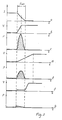
- FIGS. 2f and 2g show the voltage or power loss at the switch when using the switch-off support device according to the invention.
- FIG. 3 shows an exemplary embodiment of the switch-off support device for the three-phase drive of a brushless DC motor.
- the resistor 6 is provided in common for all six electronic switches, while the Zener diode 5 and a Zener diode 7 are each assigned to upper and lower switches, respectively.
- Slow diode 4 and slow diodes 8, 9, 10, 11 and 12 are individually connected to the electronic switches.
- the mode of operation of the switch-off support device is as follows: When the electronic switch 3 is switched off, the current flowing over it begins to drop and the voltage which would cause a countercurrent via the slow diode 4, which is biased in the forward direction via the resistor and the Zener diode 5, increases. Through this bias the further increase in the voltage is prevented until the blocking resistance of the slow or slow diode 4 is restored. The switch-off process thus takes place at a voltage which is very low compared to the voltage at the switched-off electronic switch and is practically constant. Until the current flowing through the electronic switch 3 is completely blocked, the load current is dynamically divided between the switch 3 and the series circuit comprising the slow diode 4 and the zener diode 5.
- this diode blocks, as a result of which the disconnection with regard to the inductive load 2 is ended.
- the electronic switch 3 is switched on, the slow diode 4 is again biased in the forward direction, after which the cycle described above is repeated.
- a shutdown support device for use in the pulsed operation of electric drives or the like, a shutdown support device is specified which ensures the shutdown of an inductively loaded electronic switch at very low voltages and low power losses and thus improved efficiency and can also be used in push-pull circuits.
- the electronic switch 3 and the inductive load 2 are connected in series to a direct current source 1.
- the cathode of a slow diode 4 is connected, the anode of which is connected to the cathode of a zener diode 5 and to one end of a resistor 6.
- the anode of the zener diode 5 and the other end of the resistor 6 are each connected to one of the poles of the direct current source 1.
Landscapes
- Electronic Switches (AREA)
- Inverter Devices (AREA)
Applications Claiming Priority (2)
| Application Number | Priority Date | Filing Date | Title |
|---|---|---|---|
| BG89375/89 | 1989-07-27 | ||
| BG8937589A BG50135A1 (en) | 1989-07-27 | 1989-07-27 | Device for elimination helping of electronic switch with inductive load |
Publications (2)
| Publication Number | Publication Date |
|---|---|
| EP0410327A2 true EP0410327A2 (fr) | 1991-01-30 |
| EP0410327A3 EP0410327A3 (en) | 1992-03-04 |
Family
ID=3922180
Family Applications (1)
| Application Number | Title | Priority Date | Filing Date |
|---|---|---|---|
| EP19900113987 Withdrawn EP0410327A3 (en) | 1989-07-27 | 1990-07-20 | Equipment for enhancing turnoff of a semiconductor switch with inductive load |
Country Status (3)
| Country | Link |
|---|---|
| EP (1) | EP0410327A3 (fr) |
| JP (1) | JPH03178571A (fr) |
| BG (1) | BG50135A1 (fr) |
Cited By (1)
| Publication number | Priority date | Publication date | Assignee | Title |
|---|---|---|---|---|
| FR2763762A1 (fr) * | 1997-05-21 | 1998-11-27 | H B Ind | Commutateur electronique sans pertes |
Family Cites Families (3)
| Publication number | Priority date | Publication date | Assignee | Title |
|---|---|---|---|---|
| US4016482A (en) * | 1975-10-31 | 1977-04-05 | International Business Machines Corporation | Pulse energy suppression network |
| GB1560337A (en) * | 1978-05-30 | 1980-02-06 | Coutant Electronics Ltd | Transistor switching circuits |
| JPS62117018A (ja) * | 1985-11-15 | 1987-05-28 | Alps Electric Co Ltd | 出力段制御回路 |
-
1989
- 1989-07-27 BG BG8937589A patent/BG50135A1/xx unknown
-
1990
- 1990-07-20 EP EP19900113987 patent/EP0410327A3/de not_active Withdrawn
- 1990-07-27 JP JP2198085A patent/JPH03178571A/ja active Pending
Cited By (2)
| Publication number | Priority date | Publication date | Assignee | Title |
|---|---|---|---|---|
| FR2763762A1 (fr) * | 1997-05-21 | 1998-11-27 | H B Ind | Commutateur electronique sans pertes |
| WO1999062175A1 (fr) * | 1997-05-21 | 1999-12-02 | Snc H.B. Industries | Commutateur electronique sans pertes |
Also Published As
| Publication number | Publication date |
|---|---|
| JPH03178571A (ja) | 1991-08-02 |
| BG50135A1 (en) | 1992-05-15 |
| EP0410327A3 (en) | 1992-03-04 |
Similar Documents
| Publication | Publication Date | Title |
|---|---|---|
| EP0241976B1 (fr) | Circuit pour générer une tension continue à partir d'une tension d'entrée sinusoidale | |
| DE2809439A1 (de) | Schaltungseinrichtung zur steuerung des basisstromes eines als schalttransistor betriebenen leistungstransistors | |
| DE3429488A1 (de) | Elektronische schaltvorrichtung | |
| DE102016123678A1 (de) | Anordnung und Verfahren zur Erzeugung einer negativen Spannung für einen High-Side-Schalter in einem Wechselrichter | |
| DE4012382C2 (fr) | ||
| DE2506196C2 (de) | Gleichstrom-Schaltvorrichtung zur Erhöhung des Spitzenstromes | |
| DE3215589C2 (fr) | ||
| DE19731836A1 (de) | Verfahren und Vorrichtung zum Ansteuern eines Abschaltthyristors | |
| EP3317967B1 (fr) | Circuit de commutation destiné à la commande d'un transistor | |
| DE19614816C1 (de) | Elektronisches Schaltnetzteil und dessen Verwendung | |
| EP0169609B1 (fr) | Montage de circuit pour commuter un courant dans une charge inductive | |
| EP0410327A2 (fr) | Equipement d'assistance au blocage d'un commutateur électronique à charge inductive | |
| DE19726765C2 (de) | Gatespannungsbegrenzung für eine Schaltungsanordnung | |
| DE3880621T2 (de) | Spannungsbegrenzungsschaltung fuer leistungstransistor und wechselrichter. | |
| DE1288194B (de) | Schaltungsanordnung zur Schnellerregung von gleichstrombetriebenen Elektromagneten | |
| EP0806827B1 (fr) | Circuit de protection contre l'inversion des bornes de la batterie | |
| EP3804136B1 (fr) | Pilotage d'un transistor bipolaire à électrode à grille isolée | |
| DE3603368C1 (en) | Circuit arrangement for a turn-off limiting network in gate-turn-off-type semiconductor components | |
| DE3501925A1 (de) | Schaltungsanordnung fuer ein halbgesteuertes elektronisches zweigpaar | |
| EP0122907A1 (fr) | Circuit de commande pour transistor de commutation | |
| DE3524522A1 (de) | Rueckspeisende beschaltung fuer elektronische zweigpaare in antiparallelschaltung | |
| DE3229426A1 (de) | Reihenschaltung zweier leistungs-halbleiterschalter | |
| DE4042378A1 (de) | Symmetrische schaltentlastungsanordnung fuer ein aus gategesteuerten halbleiterschaltern gebildetes wechselrichterzweigpaar | |
| DE4033348A1 (de) | Thyristorsteuerschaltung | |
| EP0840433B1 (fr) | Alimentation de tension pour le circuit de commande d'un commutateur dans un convertisseur avec circuit intermédiaire de tension |
Legal Events
| Date | Code | Title | Description |
|---|---|---|---|
| PUAI | Public reference made under article 153(3) epc to a published international application that has entered the european phase |
Free format text: ORIGINAL CODE: 0009012 |
|
| AK | Designated contracting states |
Kind code of ref document: A2 Designated state(s): DE FR GB IT NL |
|
| PUAL | Search report despatched |
Free format text: ORIGINAL CODE: 0009013 |
|
| AK | Designated contracting states |
Kind code of ref document: A3 Designated state(s): DE FR GB IT NL |
|
| STAA | Information on the status of an ep patent application or granted ep patent |
Free format text: STATUS: THE APPLICATION HAS BEEN WITHDRAWN |
|
| 18W | Application withdrawn |
Withdrawal date: 19920313 |