EP0410399B1 - Circuit pré-amplificateur vidéo - Google Patents
Circuit pré-amplificateur vidéo Download PDFInfo
- Publication number
- EP0410399B1 EP0410399B1 EP90114205A EP90114205A EP0410399B1 EP 0410399 B1 EP0410399 B1 EP 0410399B1 EP 90114205 A EP90114205 A EP 90114205A EP 90114205 A EP90114205 A EP 90114205A EP 0410399 B1 EP0410399 B1 EP 0410399B1
- Authority
- EP
- European Patent Office
- Prior art keywords
- cable
- amplifier
- compensation
- video
- input
- Prior art date
- Legal status (The legal status is an assumption and is not a legal conclusion. Google has not performed a legal analysis and makes no representation as to the accuracy of the status listed.)
- Expired - Lifetime
Links
- 230000002238 attenuated effect Effects 0.000 claims description 5
- 230000008878 coupling Effects 0.000 claims description 3
- 238000010168 coupling process Methods 0.000 claims description 3
- 238000005859 coupling reaction Methods 0.000 claims description 3
- 238000010586 diagram Methods 0.000 description 6
- 230000004044 response Effects 0.000 description 6
- 230000008901 benefit Effects 0.000 description 5
- 238000000034 method Methods 0.000 description 4
- 230000008569 process Effects 0.000 description 4
- 239000004065 semiconductor Substances 0.000 description 4
- 238000012545 processing Methods 0.000 description 3
- 230000005540 biological transmission Effects 0.000 description 2
- 238000012546 transfer Methods 0.000 description 2
- 230000004913 activation Effects 0.000 description 1
- 238000013459 approach Methods 0.000 description 1
- 239000003990 capacitor Substances 0.000 description 1
- 230000000295 complement effect Effects 0.000 description 1
- 239000002131 composite material Substances 0.000 description 1
- 238000012937 correction Methods 0.000 description 1
- 230000000593 degrading effect Effects 0.000 description 1
- 238000001914 filtration Methods 0.000 description 1
- 238000004806 packaging method and process Methods 0.000 description 1
- 238000005070 sampling Methods 0.000 description 1
- 238000012360 testing method Methods 0.000 description 1
Images



Classifications
-
- H—ELECTRICITY
- H04—ELECTRIC COMMUNICATION TECHNIQUE
- H04N—PICTORIAL COMMUNICATION, e.g. TELEVISION
- H04N7/00—Television systems
- H04N7/10—Adaptations for transmission by electrical cable
- H04N7/102—Circuits therefor, e.g. noise reducers, equalisers, amplifiers
-
- H—ELECTRICITY
- H03—ELECTRONIC CIRCUITRY
- H03F—AMPLIFIERS
- H03F3/00—Amplifiers with only discharge tubes or only semiconductor devices as amplifying elements
- H03F3/72—Gated amplifiers, i.e. amplifiers which are rendered operative or inoperative by means of a control signal
-
- H—ELECTRICITY
- H04—ELECTRIC COMMUNICATION TECHNIQUE
- H04N—PICTORIAL COMMUNICATION, e.g. TELEVISION
- H04N5/00—Details of television systems
- H04N5/14—Picture signal circuitry for video frequency region
- H04N5/148—Video amplifiers
Definitions
- the present invention relates to a high speed, variable gain video preamplifier circuit for amplifying video signals carried by a cable of a given length, the preamplifier circuit having an output for coupling the preamplified signals to a raster scan video display, said preamplifier circuit comprising an integrated circuit device including at least one output pad for connection to the video display, including:
- Such a circuit is known from document US-A- 4,148,069.
- one fixed gain amplifier is provided which may be selectively connected into or separated from the transmission line so as to provide a coarse adjustment of the gain to the transmitted signal.
- the switching of the amplifier is controlled by a cable attenuation detector.
- document EP-A-0 084 628 discloses a circuitry for equalizing automatically for attenuations of signals travelling over video transmission lines. To this end, a certain number of alternating amplifying and equalizing networks are connected in series between the output port of the cable and the input port of the next following device.
- the transfer functions of the networks are controlled in view of the length of the cable, so that the influence of the attenuation characteristics of the cable is compensated for.
- the individual transfer functions are adapted to the attenuation characteristics of the cable.
- High resolution monochrome or color raster scan video displays are finding use in an increasing number of applications. It is envisioned that the newer video displays will employ more raster scan lines (for example, 2,000 x 2,000 lines) in order to increase resolution. Such displays will require high speed operation of the driver circuitry including preamplifiers to adequately process the increased number of scan lines.
- High speed video preamplifiers are known for use with raster display drivers.
- the prior preamplifier circuits have limited common-mode signal rejection input ranges which is mainly due to semiconductor process limitations while having no provision for accepting more than one video input source or for providing any internal cable compensation.
- the ability to accept multiple video input sources without loss of signal strength increases the flexibility of a preamplifier.
- a higher common mode input range increases the effectiveness of filtering out noise. It is well known that when video signals are carried over cables of long lengths the signal can be significantly attenuated. Presently, correction of such attenuation requires complex circuitry necessary to duplicate the mathmatical error function of attenuation.
- said cable compensation means comprises a plurality of amplifier networks having a given gain
- said selection means connects selected amplifier networks together as a function of the length of the cable
- multiplexer means are provided for selectively connecting an output of one amplifier network to the variable gain amplifier means.
- the device tailors the amount of compensation for different lengths of cables by providing multiple, selectable amounts of compensation, thus using approximate compensation for cable attenuation rather than precise, complex compensation.
- a high speed, variable gain video preamplifier circuit for amplifying video signals carried by a cable.
- the preamplifier circuit has an output that can be coupled to a raster scan video display.
- the preamplifier circuit can be implemented in a single integrated circuit device form that has a plurality of input pads and at least one output pad for connection to the display. Provision is made for providing information to the integrated circuit device related to the length of the cable that carries the video signal. Compensation circuitry is provided for compensating for the attenuation characteristics of that given length of cable. This circuitry is relatively simple, compensating for attenuation, while increasing the speed of circuit operation.
- the preamplifier circuit further includes provision for accepting two different input video channels and means for selecting one of them for further processing at a broad common input range. This circuit increases flexibility of operation while operating at relatively high speed with better processing ability.
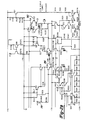
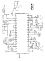
- FIGS. 1 and 4 the present invention has been designed so that it can be implemented in integrated circuit form providing all of the advantages that will become apparent to those skilled in the art after having the benefit of reading the following description and studying the drawings.
- the integrated circuit device 10 is shown packaged in a 32 pin hybrid package having a plurality of input and output terminals or pads. External circuitry provides signals to the internal circuitry on the semiconductor chip contained within the device 10 through the input pads.
- FIG. 1 shows a block diagram of the internal circuitry on the semiconductor device chip. in FIG. 1, the squares represent input and output pads. Two of the input pads 12 and 14 receive the input video signal which is carried by a first cable 16. It is a feature of this invention that the preamplifier circuitry can accept more than one video input source.
- pads 18 and 20 are shown as coupled to a channel 2 video input carried by a second cable 22.
- a channel select pad 24 receives an externally applied signal for selecting between the channel 1 video on cable 16 or the channel 2 video carried on cable 22.
- the signal on pad 24 operates to cause switching circuitry 26 to select either the channel 1 or channel 2 video input signal for further processing by the preamplifier circuitry.
- the video signal is typically derived from a variety of sources such as video test pattern generator and carried over various lengths of cables to the preamplifier device 10.
- the preamplifier device 10 will be part of a video channel which consists of preamplifier and video amplifier circuitry.
- the video signal may be carried over cables of very long lengths. It is known that the video signal will be attenuated or degraded when it is carried over long lengths of cable. Cables of longer lengths, of course, will attenuate the signal more than cables of shorter lengths. It is a feature of this invention that the integrated circuit device 10 compensates for this attenuation of the signal and, moreover, it tailors the amount of compensation for different lengths of cables by providing multiple, selectable amounts of compensation.
- compensation for cable lengths in three different ranges is provided: namely, a range of 0-333 feet, a range of 333-666 feet and a range of 666-1000 feet.
- This invention is not limited to only three ranges, more or fewer ranges may be provided depending upon the application.
- Three separate input pads 28, 30 and 32 are provided to supply information related to the length of the cable being used. In the preferred embodiment, this information takes the form quite simply of a logical high or low signal applied to the appropriate pad.
- These selection signals control a 3:1 multiplexer 34.
- Multiplexer 34 is connected between the cable compensation circuitry and a gain controlled variable preamplifier generally designated by the numeral 36.
- Variable preamplifier 36 serves to amplify the compensated signal as a function of the gain control input on pad 38. The amplified signal is then output over pad 40 to the raster scan display.
- the cable compensation network in this embodiment includes, for each video input channels, a common set of three series-connected amplifiers 42(a-b), 44 and 46. Each amplifier has its own external compensating network coupled to it through input pads on the device 10.
- Z-Compensation (Z-Comp) circuitry 48 is coupled to amplifier 42a.
- Substantially identical external Z-Comp circuitry 50 is coupled to amplifier 42b.
- Z-Comp external circuitry 52 is coupled to amplifier 44 whereas external Z-Comp circuitry 54 is coupled to amplifier 46.
- the external Z-Comp circuitry cooperates with the on-chip amplifier to vary the gain such that in one embodiment, it allows unity gain at DC and a high frequency gain of 6DB.
- the Z-Comp circuitry cooperates with the on-chip amplifier to produce an output gain response complementary to the loss response of a typical 333 foot coaxial cable. The resultant overall response is thus flat in said frequency range.
- the circuitry is formed on a single integrated circuit and the amplifiers 42(a-b), 44 and 46 and their external Z-Comp circuitry 48, 50, 52 and 54 are matched or are substantially identical. Thus, they provide substantially identical degrees of compensation.
- the present invention overcomes previous difficulties in continuously compensating long lengths of coaxial cables by dividing the compensation into segments, in this case three 333 feet segments. If the selected length of cable falls within the 0-333 foot range, an appropriate signal is applied to input pad 28 to cause the multiplexer 34 to couple input line 56 to the output line 58. Assuming, for example, that the channel 1 video has been selected, this means that the output of amplifier 42b on line 60 is coupled to the variable amplifier circuitry 36.
- Amplifier 42b and its Z-Comp circuitry 50 have compensated for the attenuation of the signal caused by the 0-333 foot long cable.
- the compensated signal thus is amplified by variable amplifier 36 and then output to the display over pad 40.
- the appropriate signal on pad 30 causes multiplexer 34 to select line 62 which is coupled to the output of amplifier 44.
- the output of amplifier 42b is added to the compensation provided by the 333-666 foot compensator amplifier 44 and associated Z-Comp circuitry 52.
- multiplexer 34 selects line 64 connected to the output of amplifier 46 if the cable is in the 666-1000 foot range as indicated by the appropriate signal on input pad 32.
- the compensation of amplifier 44 as well as that of amplifier 42b is added to that of amplifier 46 and its external Z-Compensation network 54.
- This cable compensation scheme overcomes the difficulty of correcting for attenuation over long cable lengths. Such difficulty was due generally to the amount of circuitry necessary to duplicate the error function of the cable response.
- the known approaches generally operated at relatively low speeds whereas the present invention can operate with a band width of in excess of 150 megahertz because of the IC packaging. All of these advantages are provided in a relatively simple manner using approximate compensation for cable attenuation rather than precise, complex compensation.
- the integrated circuit device 10 also includes other functions usually found in preamplifier circuits.
- a sample and hold circuit generally designated by the numeral 66 operates to stabilize the video black level. It does this by sampling the video at the cathode of the CRT being driven during the time necessary for the sample hold circuit to restore the video image to the predetermined DC level, so called back porch time, and forcing it to remain constant.
- the gain controlled variable gain amplifier circuitry 36 operates by receiving three signals. First it receives the cable compensated video signal from the 3:1 MUX 34; second, it receives a DC gain control signal from pad 38 (pin 19, FIG. 4) to set the video peak to peak swing on output pad 40 (pin 9, FIG. 1) to an operator desired amplitude; third, it receives a DC S/H signal from the S/H amplifier 66 to stabilize the back porch level of the video signal at output pad 40, corresponding to the video amplifier output DC level (video amplifier not shown).
- amplifier 68 provides an output on pad 70 (pin 3, FIG. 4) by taking the input composite video and amplifying said sync signal.
- the sync output on pad 70 can be used for synchronization stripping.
- an external jumper 72 may be inserted to bypass cable compensation amplifiers 44 and 46 and the multiplexer 34 for maximum bandwidth operation by relying solely on the input amplifiers 42a or 42b.
- the input stage consists of two differential pairs that share a common load R8.
- the gain is set via an external resistor bridging the two channel 1 and channel 2 Z-Comp input pads 82, 84 and 86, 88, respectively.
- the common mode signal (7.0 volts peak to peak maximum) is distributed across several transistors which are in a stacked common-base configuration.
- Common-base stages Q11, Q13 are used to float the differential pair.
- a Darlington configuration consisting of transistors Q5 and Q11 reduces the impedance of the base of transistor Q11 thereby increasing bandwidth.
- the channel select function is accomplished by engaging the appropriate pair of current sources (Q36/Q37 or Q39/Q40) via current steering.
- the open collector TTL channel select input 82 sets the DC bias at the base of transistor Q36/Q37 either above (channel 1 selected) or below (channel 2 selected) the constant DC bias on the base of transistor Q39/Q40.
- either the video signal provided to the channel 1 or channel 2 input pads 74, 76 or 78, 80 are coupled through load R8 which in turn drives the transistor Q9.
- External Z-Comp circuitry 48 and 50 are coupled to input pads 82, 84 and 86, 88 to provide the cable compensation in the 0-333 foot range depending upon whether channel 1 or channel 2 is selected.
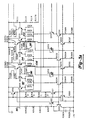
- the output of transistor Q9 is coupled to line 90 in FIG. 3A which shows the details of the compensating amplifiers for the other two ranges, as well as the multiplexer 34.
- the amplifier 44 for the 333-666 foot range and the amplifier 46 for the 666-1000 foot range are provided by two cascaded feedback amplifier stages generally designated by the numerals 92 and 94. The DC gain of each stage is unity allowing DC coupling.
- Emitter resistors in the differential pairs lower the open loop gain which increase the unity gain phase margin to 70 degrees without degrading the slew rate performance at the output.
- External Z-Comp network 52 is coupled to pad 96 whereas the Z-Comp circuitry 54 for the 666-1000 foot range is coupled to input pad 98. It will be remembered that the 0-333 foot cable compensation for either the channel 1 or channel 2 video has been accomplished in connection with the amplifiers discussed in FIG. 2. Thus, the signal on line 90 has already been compensated for cables in the 0-333 foot range.
- Multiplexer 34 is implemented with three multiplexer amplifiers generally designated by the numerals 100, 102 and 104. These three mux amplifiers share a common output transistor Q208. Three input transistors Q201, Q202 and Q203 receive selection signals from pads 28, 30 and 32, respectively. These transistors with internal pull-ups for open collector TTL operation are used to steer the common current source provided by transistor Q226. External logic ensures that one and only one TTL input on pads 28, 30 and 32 is high at all times. Depending upon which mux amplifier is engaged, cable compensation for the three aforementioned increments are selected.
- mux amplifier 104 will conduct thereby connecting only the signal on line 90 to the output transistor Q208.
- Activation of mux amplifier 102 will couple the output of compensation amplifier 92 to the output transistor Q208 over output line 106 whereas engagement of mux amp 100 will couple the output of compensation amplifier 94 on line 108 to the output transistor.
- Output transistor Q208 is, in turn, coupled to the preamplifier circuitry 36 via an external capacitor. As discussed, the preamplifier circuitry 36 amplifies the compensated signal and supplies it over output pad 40 (pin 9, FIG. 1) to the driver of the raster scan display.
- the present invention provides significant advantages over the prior art. It can process video signals driven over long lengths of cables at a video bandwidth of at least 150 megahertz using a segmented video cable compensation scheme.
- Two video channels can be selected with 7.0 volts peak to peak of common mode signal rejection on each channel.
- a floating bias scheme is used to thereby circumvent semiconductor process limitations which are often limited to 5.5 volts peak to peak. All of the channel and cable compensation switching is TTL compatible for simple automatic/computer interface.
- the integrated circuit can be used to drive monochrome/color displays with or without cable compensation.
- the three segmented cable compensation scheme reduces a previously complex compensation problem in building complex circuitry to duplicate the cable response error function to a simple one of approximating a response thereby saving chip space for the rest of the integrated circuit system.
Landscapes
- Engineering & Computer Science (AREA)
- Multimedia (AREA)
- Signal Processing (AREA)
- Power Engineering (AREA)
- Picture Signal Circuits (AREA)
- Control Of Amplification And Gain Control (AREA)
- Details Of Television Systems (AREA)
Claims (10)
- Circuit préamplificateur vidéo à gain variable, fonctionnant à grande vitesse pour amplifier des signaux vidéo véhiculés par un câble (16,22) d'une longueur donnée, le circuit préamplificateur possédant une sortie pour appliquer les signaux préamplifiés à un dispositif d'affichage vidéo à balayage de trame, ledit circuit préamplificateur comprenant un dispositif à circuits intégrés (10) contenant au moins un plot de sortie (40) pour la connexion au dispositif d'affichage vidéo, comprenant :- des moyens de sélection (28 - 34) possédant au moins un plot d'entrée (28,30,32) pour recevoir une information concernant la longueur du câble (16,22);- des moyens (42 - 54) de compensation du câble pour produire de façon sélective un gain accru pour le signal vidéo reçu afin de compenser l'atténuation du signal vidéo, due à la longueur du câble (16, 22); et- des moyens formant amplificateur à gain variable (36) branchés entre les moyens (42 - 54) de compensation du câble et ledit plot de sortie (40) pour amplifier le signal compensé fourni par les moyens (42 - 54) de compensation du câble,caractérisé en ce que- lesdits moyens (42 - 54) de compensation du câble comprennent une pluralité de réseaux amplificateurs (42, 44, 46) possédant un gain donné;- lesdits moyens de sélection (28 - 34) raccordent entre eux des réseaux amplificateurs sélectionnés (42, 44, 46), en fonction de la longueur du câble (16, 22), et- des moyens formant multiplexeur (34) sont prévus pour connecter de façon sélective une sortie d'un réseau amplificateur (42, 44, 46) aux moyens (36) formant amplificateur à gain variable.
- Circuit selon la revendication 1, caractérisé en ce que les réseaux amplificateurs (42, 44, 46) peuvent être branchés en série de telle sorte que le signal vidéo est amplifié d'une valeur donnée dans chaque réseau (42, 44, 46).
- Circuit selon l'une quelconque des revendications 1 ou 2, caractérisé en ce que :- lesdits moyens (42 - 54) de compensation du câble incluent un premier amplificateur (42a, 42b) pour amplifier des signaux vidéo qui ont été atténués par les longueurs de câble de 0 - 333 pieds (0 - 102 m); un deuxième amplificateur (44) branché en série avec ledit premier amplificateur (42a, 42b) et coopérant avec ce dernier pour compenser des signaux qui ont été atténués par des câbles de 333 - 666 pieds (102 - 204 m); et un troisième amplificateur (46) branché en série avec lesdits premier et second amplificateurs (42a, 42b, 44) et coopérant avec ces derniers pour compenser des signaux vidéo qui ont été atténués par des longueurs de câble de 666 - 1000 pieds (204 - 305 m);- lesdits moyens de sélection (28 - 34) comprennent en outre un premier plot d'entrée (28) associé à des longueurs de câble de 0 - 333 pieds (0 - 102 m); un deuxième plot d'entrée (30) associé à des longueurs de câble de 333 - 666 pieds (102 - 204 m) ; et un troisième plot d'entrée (32) associé à des longueurs de câble de 666 - 1000 pieds (204 - 205 m), et- ledit dispositif à circuits intégrés (10) comprend en outre un multiplexeur (34) comportant des entrées connectées auxdits premier, deuxième et troisième plots d'entrée (28, 30, 32), ledit multiplexeur (34) étant adapté pour connecter une sortie du premier, deuxième ou troisième amplificateur (42a, 42b, 44, 46) à une entrée des moyens formant amplificateur variable (36) en fonction de signaux de sélection appliqués aux premier, deuxième ou troisième plot d'entrée (28, 30, 32) du multiplexeur.
- Circuit selon l'une quelconque des revendications 1 à 3, caractérisé par :- un premier couple de plots d'entrée (12, 14) pour recevoir des signaux vidéo véhiculés par un premier câble (16) ;- un second couple de plots d'entrée (18, 20) pour recevoir différents signaux vidéo véhiculés par un second câble (22); et- des moyens (24, 26) pour effectuer une sélection entre les signaux vidéo dans le premier ou le second câble (16, 22), le circuit intégré pouvant être utilisé pour préamplifier deux canaux d'entrée vidéo différents.
- Circuit selon la revendication 1, caractérisé par :- ledit circuit intégré (10) possédant un premier ensemble de plots d'entrée vidéo (12, 14) pour recevoir un premier canal vidéo véhiculé par un premier câble (16) ;- un second ensemble de plots d'entrée vidéo (18, 20) pour recevoir un second canal vidéo véhiculé par un second câble (22); et- des moyens de commutation (24, 26) pour connecter de façon sélective le premier ou le second canal vidéo aux moyens formant amplificateur variable (36).
- Circuit préamplificateur selon la revendication 5, caractérisé en ce que lesdits moyens (42 - 54) de compensation du câble comprennent :- un premier amplificateur de compensation (42b) pour le premier canal vidéo, ledit premier amplificateur de compensation (42b) compensant l'atténuation du signal dans le premier canal vidéo produite par un câble (16) possédant une longueur située dans une gamme donnée, le premier amplificateur de compensation (42b) possédant une sortie;- un deuxième amplificateur de compensation (42a) connecté au second ensemble de plots d'entrée (18,20) pour compenser une atténuation du signal dans le second canal vidéo produite par des câbles (22) ayant des longueurs situées dans ladite gamme donnée, ledit deuxième amplificateur de compensation (42a) possédant une sortie;- un troisième amplificateur de compensation (44) pour compenser une atténuation du signal produite par des câbles (16, 22) ayant des longueurs situées dans une seconde gamme; et- lesdits moyens de commutation (24, 26) connectant de façon sélective les sorties desdits premier ou deuxième amplificateurs de compensation (42b, 42a) à une entrée du troisième amplificateur de compensation (44).
- Circuit selon la revendication 6, caractérisé par :- un quatrième amplificateur de compensation (46) pour compenser une atténuation du signal pour des câbles (16, 22) ayant une longueur encore plus importante que dans le cas du troisième amplificateur de compensation (44);- des moyens formant multiplexeur (34) pour connecter de façon sélective des sorties du premier ou du deuxième, du troisième et du quatrième amplificateurs de compensation (42b, 42a, 44, 46) aux moyens formant amplificateur variable (36) en fonction de la longueur de câble (16, 22) utilisée pour véhiculer les premier ou second signaux des canaux vidéo.
- Circuit selon la revendication 7, caractérisé en ce que les troisième et quatrième circuits amplificateurs de compensation (44, 46) sont connectés en série entre eux, les premier et deuxième amplificateurs de compensation (42b, 42a) étant connectés en série avec l'entrée du troisième amplificateur de compensation (44); les moyens formant multiplexeur (34) raccordant de façon sélective des sorties des amplificateurs de compensation (42a, 42b, 44, 46) à l'amplificateur à gain variable (36) en fonction de la longueur du câble (16, 22).
- Circuit selon la revendication 7, caractérisé en ce que :- lesdits moyens formant multiplexeur (28 - 34) raccordent de façon sélective la sortie du premier ou du deuxième, du troisième et du quatrième amplificateurs de compensation (42b, 42a, 44, 46) à l'entrée de l'amplificateur à gain variable (36), ce qui a pour effet que des signaux vidéo présents dans le premier ou le second câble (16, 22) sont préamplifiés et l'atténuation du signal produite par le câble sélectionné (16, 22) est compensée grâce à l'utilisation du multiplexeur (34) servant à connecter la sortie appropriée des amplificateurs de compensation (42a, 42b, 44, 46) à l'amplificateur variable (36) en fonction de la longueur du câble (16, 22).
- Circuit selon la revendication 9, réalisé sous la forme d'un circuit intégré.
Applications Claiming Priority (2)
| Application Number | Priority Date | Filing Date | Title |
|---|---|---|---|
| US07/386,384 US4984079A (en) | 1989-07-26 | 1989-07-26 | Video preamplifier circuit |
| US386384 | 1995-02-10 |
Publications (3)
| Publication Number | Publication Date |
|---|---|
| EP0410399A2 EP0410399A2 (fr) | 1991-01-30 |
| EP0410399A3 EP0410399A3 (en) | 1992-05-06 |
| EP0410399B1 true EP0410399B1 (fr) | 1996-08-28 |
Family
ID=23525369
Family Applications (1)
| Application Number | Title | Priority Date | Filing Date |
|---|---|---|---|
| EP90114205A Expired - Lifetime EP0410399B1 (fr) | 1989-07-26 | 1990-07-25 | Circuit pré-amplificateur vidéo |
Country Status (5)
| Country | Link |
|---|---|
| US (1) | US4984079A (fr) |
| EP (1) | EP0410399B1 (fr) |
| JP (1) | JPH0373673A (fr) |
| CA (1) | CA2019393C (fr) |
| DE (1) | DE69028258T2 (fr) |
Families Citing this family (14)
| Publication number | Priority date | Publication date | Assignee | Title |
|---|---|---|---|---|
| DE4140112A1 (de) * | 1991-12-05 | 1993-06-09 | Leybold Ag, 6450 Hanau, De | Verfahren und schaltung zur messung von teilchenstroemen |
| FR2685832B1 (fr) * | 1991-12-31 | 1994-02-11 | Thomson Broadcast | Systeme correcteur de lignes de transmission. |
| DE69327986T2 (de) * | 1992-06-03 | 2000-10-05 | Koninklijke Philips Electronics N.V., Eindhoven | System zur automatischen Kompensation der Kabeldämpfung |
| US5432562A (en) * | 1993-01-26 | 1995-07-11 | U.S. Philips Corporation | Television signal reception |
| CN1066594C (zh) * | 1995-09-19 | 2001-05-30 | 沈来沛 | 视频电线电缆长距离传输校正系统 |
| US6115418A (en) | 1998-02-09 | 2000-09-05 | National Semiconductor Corporation | Simplified equalizer for twisted pair channel |
| US6415003B1 (en) | 1998-09-11 | 2002-07-02 | National Semiconductor Corporation | Digital baseline wander correction circuit |
| US6438163B1 (en) * | 1998-09-25 | 2002-08-20 | National Semiconductor Corporation | Cable length and quality indicator |
| US6418172B1 (en) | 1999-04-21 | 2002-07-09 | National Semiconductor Corporation | Look-ahead maximum likelihood sequence estimation decoder |
| US7254198B1 (en) | 2000-04-28 | 2007-08-07 | National Semiconductor Corporation | Receiver system having analog pre-filter and digital equalizer |
| US7050517B1 (en) | 2000-04-28 | 2006-05-23 | National Semiconductor Corporation | System and method suitable for receiving gigabit ethernet signals |
| JP4426222B2 (ja) * | 2003-07-10 | 2010-03-03 | 興和株式会社 | ケーブル延長装置 |
| EP2479889B1 (fr) * | 2011-01-19 | 2014-03-19 | Alcatel Lucent | Système amplificateur et son procédé de fonctionnement |
| US9584041B2 (en) * | 2013-08-26 | 2017-02-28 | Google Technology Holdings LLC | Method and apparatus for charging devices using a multiple port power supply |
Family Cites Families (9)
| Publication number | Priority date | Publication date | Assignee | Title |
|---|---|---|---|---|
| FR2302632A1 (fr) * | 1975-02-27 | 1976-09-24 | Stem Electronique | Commutateur cyclique |
| US4032974A (en) * | 1975-10-20 | 1977-06-28 | North American Philips Corporation | Video processing circuit |
| US4148069A (en) * | 1977-02-14 | 1979-04-03 | Harris Corporation | Automatic cable loss compensator for use in a television camera system |
| US4220931A (en) * | 1978-05-12 | 1980-09-02 | Northern Telecom Systems Corporation | Composite video automatic gain control amplifier |
| US4214261A (en) * | 1979-01-11 | 1980-07-22 | Rca Corporation | Synchronizing apparatus for remote television apparatus |
| US4404551A (en) * | 1981-04-14 | 1983-09-13 | Reuters Limited | Plural video keyboard access system |
| DE3148242A1 (de) * | 1981-12-05 | 1983-06-09 | Robert Bosch Gmbh, 7000 Stuttgart | Kabelentzerrerschaltung |
| FR2555839B1 (fr) * | 1983-11-25 | 1986-01-24 | Thomson Csf | Dispositif amplificateur-limiteur a large bande |
| JPS60248031A (ja) * | 1984-05-24 | 1985-12-07 | Nec Corp | 自動等化器 |
-
1989
- 1989-07-26 US US07/386,384 patent/US4984079A/en not_active Expired - Fee Related
-
1990
- 1990-06-20 CA CA002019393A patent/CA2019393C/fr not_active Expired - Fee Related
- 1990-07-25 DE DE69028258T patent/DE69028258T2/de not_active Expired - Fee Related
- 1990-07-25 EP EP90114205A patent/EP0410399B1/fr not_active Expired - Lifetime
- 1990-07-26 JP JP2198948A patent/JPH0373673A/ja active Pending
Also Published As
| Publication number | Publication date |
|---|---|
| EP0410399A3 (en) | 1992-05-06 |
| CA2019393C (fr) | 1995-01-03 |
| JPH0373673A (ja) | 1991-03-28 |
| CA2019393A1 (fr) | 1991-01-26 |
| DE69028258T2 (de) | 1997-03-27 |
| EP0410399A2 (fr) | 1991-01-30 |
| DE69028258D1 (de) | 1996-10-02 |
| US4984079A (en) | 1991-01-08 |
Similar Documents
| Publication | Publication Date | Title |
|---|---|---|
| EP0410399B1 (fr) | Circuit pré-amplificateur vidéo | |
| US5410363A (en) | Automatic gain control device for transmitting video signals between two locations by use of a known reference pulse during vertical blanking period so as to control the gain of the video signals at the second location | |
| US4148069A (en) | Automatic cable loss compensator for use in a television camera system | |
| US6081362A (en) | Optical receiver capable of responding to both burst and continuous signals | |
| US4564818A (en) | Transimpedance amplifier having an improved gain/bandwidth product | |
| CA1049648A (fr) | Melangeur de signaux electroniques | |
| EP0134008A2 (fr) | Procédé et dispositif de synchronisation extérieure pour système de transmission d'information | |
| US6150997A (en) | Video transmission system | |
| US4647973A (en) | Switch apparatus for a video interconnection system | |
| US6184919B1 (en) | Extended length differentially driven analog video link | |
| US4993045A (en) | Modem diagnostic loop | |
| US4677481A (en) | Dual display monitor | |
| US6937294B1 (en) | Multiplexed video signal interface signal, system and method | |
| US4604589A (en) | High frequency circuit | |
| US6377629B1 (en) | Twisted pair communications line system | |
| US7206348B2 (en) | Twisted pair communications line system | |
| KR970003720B1 (ko) | 전기신호 증폭기 장치 | |
| EP1179222A1 (fr) | Amplificateur de puissance radioelectrique avec retour du port d'isolation d'un coupleur hybride | |
| US6348902B1 (en) | Display device having pass-through function for picture signal | |
| US7643018B1 (en) | Twisted pair communications line system | |
| US5864371A (en) | Luminance signal generation circuit with single clamp in closed loop configuration and horizontal synchronization pulse generation | |
| US5030896A (en) | D.C. restore for a remote video interconnect | |
| US4641063A (en) | Video driver level shifter | |
| ES8601621A1 (es) | Perfeccionamientos introducidos en un dispositivo de tratamiento de senales de video | |
| US3969579A (en) | Contrast, brightness and peaking control circuit |
Legal Events
| Date | Code | Title | Description |
|---|---|---|---|
| PUAI | Public reference made under article 153(3) epc to a published international application that has entered the european phase |
Free format text: ORIGINAL CODE: 0009012 |
|
| AK | Designated contracting states |
Kind code of ref document: A2 Designated state(s): DE FR GB NL |
|
| PUAL | Search report despatched |
Free format text: ORIGINAL CODE: 0009013 |
|
| AK | Designated contracting states |
Kind code of ref document: A3 Designated state(s): DE FR GB NL |
|
| 17P | Request for examination filed |
Effective date: 19921028 |
|
| 17Q | First examination report despatched |
Effective date: 19940725 |
|
| GRAH | Despatch of communication of intention to grant a patent |
Free format text: ORIGINAL CODE: EPIDOS IGRA |
|
| GRAH | Despatch of communication of intention to grant a patent |
Free format text: ORIGINAL CODE: EPIDOS IGRA |
|
| GRAA | (expected) grant |
Free format text: ORIGINAL CODE: 0009210 |
|
| AK | Designated contracting states |
Kind code of ref document: B1 Designated state(s): DE FR GB NL |
|
| REF | Corresponds to: |
Ref document number: 69028258 Country of ref document: DE Date of ref document: 19961002 |
|
| ET | Fr: translation filed | ||
| PLBE | No opposition filed within time limit |
Free format text: ORIGINAL CODE: 0009261 |
|
| STAA | Information on the status of an ep patent application or granted ep patent |
Free format text: STATUS: NO OPPOSITION FILED WITHIN TIME LIMIT |
|
| 26N | No opposition filed | ||
| REG | Reference to a national code |
Ref country code: GB Ref legal event code: 732E |
|
| NLS | Nl: assignments of ep-patents |
Owner name: RAYTHEON COMPANY;HE HOLDINGS, INC. |
|
| REG | Reference to a national code |
Ref country code: FR Ref legal event code: TP Ref country code: FR Ref legal event code: CD Ref country code: FR Ref legal event code: CA |
|
| PGFP | Annual fee paid to national office [announced via postgrant information from national office to epo] |
Ref country code: FR Payment date: 20010702 Year of fee payment: 12 |
|
| PGFP | Annual fee paid to national office [announced via postgrant information from national office to epo] |
Ref country code: GB Payment date: 20010703 Year of fee payment: 12 Ref country code: DE Payment date: 20010703 Year of fee payment: 12 |
|
| PGFP | Annual fee paid to national office [announced via postgrant information from national office to epo] |
Ref country code: NL Payment date: 20010717 Year of fee payment: 12 |
|
| REG | Reference to a national code |
Ref country code: GB Ref legal event code: IF02 |
|
| PG25 | Lapsed in a contracting state [announced via postgrant information from national office to epo] |
Ref country code: GB Free format text: LAPSE BECAUSE OF NON-PAYMENT OF DUE FEES Effective date: 20020725 |
|
| PG25 | Lapsed in a contracting state [announced via postgrant information from national office to epo] |
Ref country code: NL Free format text: LAPSE BECAUSE OF NON-PAYMENT OF DUE FEES Effective date: 20030201 Ref country code: DE Free format text: LAPSE BECAUSE OF NON-PAYMENT OF DUE FEES Effective date: 20030201 |
|
| GBPC | Gb: european patent ceased through non-payment of renewal fee |
Effective date: 20020725 |
|
| PG25 | Lapsed in a contracting state [announced via postgrant information from national office to epo] |
Ref country code: FR Free format text: LAPSE BECAUSE OF NON-PAYMENT OF DUE FEES Effective date: 20030331 |
|
| NLV4 | Nl: lapsed or anulled due to non-payment of the annual fee |
Effective date: 20030201 |
|
| REG | Reference to a national code |
Ref country code: FR Ref legal event code: ST |