EP0410656B1 - Elektrisch lösbare Verbindung mit hoher Kontaktdichte - Google Patents
Elektrisch lösbare Verbindung mit hoher Kontaktdichte Download PDFInfo
- Publication number
- EP0410656B1 EP0410656B1 EP90307986A EP90307986A EP0410656B1 EP 0410656 B1 EP0410656 B1 EP 0410656B1 EP 90307986 A EP90307986 A EP 90307986A EP 90307986 A EP90307986 A EP 90307986A EP 0410656 B1 EP0410656 B1 EP 0410656B1
- Authority
- EP
- European Patent Office
- Prior art keywords
- contact pads
- pads
- traces
- support
- contact
- Prior art date
- Legal status (The legal status is an assumption and is not a legal conclusion. Google has not performed a legal analysis and makes no representation as to the accuracy of the status listed.)
- Expired - Lifetime
Links
- 239000003086 colorant Substances 0.000 claims description 15
- 239000000463 material Substances 0.000 claims description 10
- 229910052751 metal Inorganic materials 0.000 claims description 9
- 239000002184 metal Substances 0.000 claims description 9
- 239000004020 conductor Substances 0.000 claims description 7
- 239000000976 ink Substances 0.000 description 21
- 238000013459 approach Methods 0.000 description 20
- 238000000034 method Methods 0.000 description 5
- 238000004519 manufacturing process Methods 0.000 description 4
- 230000007246 mechanism Effects 0.000 description 4
- 230000008901 benefit Effects 0.000 description 3
- 238000011109 contamination Methods 0.000 description 3
- 230000000694 effects Effects 0.000 description 3
- 229920001971 elastomer Polymers 0.000 description 3
- 239000000806 elastomer Substances 0.000 description 3
- 238000007747 plating Methods 0.000 description 3
- 230000009467 reduction Effects 0.000 description 3
- RYGMFSIKBFXOCR-UHFFFAOYSA-N Copper Chemical compound [Cu] RYGMFSIKBFXOCR-UHFFFAOYSA-N 0.000 description 2
- PXHVJJICTQNCMI-UHFFFAOYSA-N Nickel Chemical compound [Ni] PXHVJJICTQNCMI-UHFFFAOYSA-N 0.000 description 2
- KDLHZDBZIXYQEI-UHFFFAOYSA-N Palladium Chemical compound [Pd] KDLHZDBZIXYQEI-UHFFFAOYSA-N 0.000 description 2
- 229910052802 copper Inorganic materials 0.000 description 2
- 239000010949 copper Substances 0.000 description 2
- 238000005260 corrosion Methods 0.000 description 2
- 230000007797 corrosion Effects 0.000 description 2
- 239000000975 dye Substances 0.000 description 2
- PCHJSUWPFVWCPO-UHFFFAOYSA-N gold Chemical compound [Au] PCHJSUWPFVWCPO-UHFFFAOYSA-N 0.000 description 2
- 229910052737 gold Inorganic materials 0.000 description 2
- 239000010931 gold Substances 0.000 description 2
- 230000006872 improvement Effects 0.000 description 2
- 238000004377 microelectronic Methods 0.000 description 2
- 239000004065 semiconductor Substances 0.000 description 2
- 239000000758 substrate Substances 0.000 description 2
- 235000001674 Agaricus brunnescens Nutrition 0.000 description 1
- 239000004411 aluminium Substances 0.000 description 1
- 229910052782 aluminium Inorganic materials 0.000 description 1
- XAGFODPZIPBFFR-UHFFFAOYSA-N aluminium Chemical compound [Al] XAGFODPZIPBFFR-UHFFFAOYSA-N 0.000 description 1
- 230000015572 biosynthetic process Effects 0.000 description 1
- 230000000295 complement effect Effects 0.000 description 1
- 150000001875 compounds Chemical group 0.000 description 1
- 239000012141 concentrate Substances 0.000 description 1
- 230000008094 contradictory effect Effects 0.000 description 1
- 230000003247 decreasing effect Effects 0.000 description 1
- 230000008021 deposition Effects 0.000 description 1
- 239000013536 elastomeric material Substances 0.000 description 1
- 239000006023 eutectic alloy Substances 0.000 description 1
- 238000000605 extraction Methods 0.000 description 1
- 239000012530 fluid Substances 0.000 description 1
- 229910052732 germanium Inorganic materials 0.000 description 1
- GNPVGFCGXDBREM-UHFFFAOYSA-N germanium atom Chemical compound [Ge] GNPVGFCGXDBREM-UHFFFAOYSA-N 0.000 description 1
- 238000000465 moulding Methods 0.000 description 1
- 229910052759 nickel Inorganic materials 0.000 description 1
- 229910052763 palladium Inorganic materials 0.000 description 1
- 229920000642 polymer Polymers 0.000 description 1
- 238000003825 pressing Methods 0.000 description 1
- 229920002379 silicone rubber Polymers 0.000 description 1
- 239000004945 silicone rubber Substances 0.000 description 1
- 229910052709 silver Inorganic materials 0.000 description 1
- 239000004332 silver Substances 0.000 description 1
Images


Classifications
-
- B—PERFORMING OPERATIONS; TRANSPORTING
- B41—PRINTING; LINING MACHINES; TYPEWRITERS; STAMPS
- B41J—TYPEWRITERS; SELECTIVE PRINTING MECHANISMS, i.e. MECHANISMS PRINTING OTHERWISE THAN FROM A FORME; CORRECTION OF TYPOGRAPHICAL ERRORS
- B41J2/00—Typewriters or selective printing mechanisms characterised by the printing or marking process for which they are designed
- B41J2/005—Typewriters or selective printing mechanisms characterised by the printing or marking process for which they are designed characterised by bringing liquid or particles selectively into contact with a printing material
- B41J2/01—Ink jet
- B41J2/135—Nozzles
- B41J2/14—Structure thereof only for on-demand ink jet heads
- B41J2/14016—Structure of bubble jet print heads
- B41J2/14072—Electrical connections, e.g. details on electrodes, connecting the chip to the outside...
-
- H—ELECTRICITY
- H01—ELECTRIC ELEMENTS
- H01R—ELECTRICALLY-CONDUCTIVE CONNECTIONS; STRUCTURAL ASSOCIATIONS OF A PLURALITY OF MUTUALLY-INSULATED ELECTRICAL CONNECTING ELEMENTS; COUPLING DEVICES; CURRENT COLLECTORS
- H01R12/00—Structural associations of a plurality of mutually-insulated electrical connecting elements, specially adapted for printed circuits, e.g. printed circuit boards [PCB], flat or ribbon cables, or like generally planar structures, e.g. terminal strips, terminal blocks; Coupling devices specially adapted for printed circuits, flat or ribbon cables, or like generally planar structures; Terminals specially adapted for contact with, or insertion into, printed circuits, flat or ribbon cables, or like generally planar structures
- H01R12/70—Coupling devices
- H01R12/71—Coupling devices for rigid printing circuits or like structures
- H01R12/712—Coupling devices for rigid printing circuits or like structures co-operating with the surface of the printed circuit or with a coupling device exclusively provided on the surface of the printed circuit
- H01R12/714—Coupling devices for rigid printing circuits or like structures co-operating with the surface of the printed circuit or with a coupling device exclusively provided on the surface of the printed circuit with contacts abutting directly the printed circuit; Button contacts therefore provided on the printed circuit
-
- B—PERFORMING OPERATIONS; TRANSPORTING
- B41—PRINTING; LINING MACHINES; TYPEWRITERS; STAMPS
- B41J—TYPEWRITERS; SELECTIVE PRINTING MECHANISMS, i.e. MECHANISMS PRINTING OTHERWISE THAN FROM A FORME; CORRECTION OF TYPOGRAPHICAL ERRORS
- B41J2/00—Typewriters or selective printing mechanisms characterised by the printing or marking process for which they are designed
- B41J2/005—Typewriters or selective printing mechanisms characterised by the printing or marking process for which they are designed characterised by bringing liquid or particles selectively into contact with a printing material
- B41J2/01—Ink jet
- B41J2/135—Nozzles
- B41J2/14—Structure thereof only for on-demand ink jet heads
- B41J2002/14387—Front shooter
-
- B—PERFORMING OPERATIONS; TRANSPORTING
- B41—PRINTING; LINING MACHINES; TYPEWRITERS; STAMPS
- B41J—TYPEWRITERS; SELECTIVE PRINTING MECHANISMS, i.e. MECHANISMS PRINTING OTHERWISE THAN FROM A FORME; CORRECTION OF TYPOGRAPHICAL ERRORS
- B41J2202/00—Embodiments of or processes related to ink-jet or thermal heads
- B41J2202/01—Embodiments of or processes related to ink-jet heads
- B41J2202/14—Mounting head into the printer
-
- Y—GENERAL TAGGING OF NEW TECHNOLOGICAL DEVELOPMENTS; GENERAL TAGGING OF CROSS-SECTIONAL TECHNOLOGIES SPANNING OVER SEVERAL SECTIONS OF THE IPC; TECHNICAL SUBJECTS COVERED BY FORMER USPC CROSS-REFERENCE ART COLLECTIONS [XRACs] AND DIGESTS
- Y10—TECHNICAL SUBJECTS COVERED BY FORMER USPC
- Y10T—TECHNICAL SUBJECTS COVERED BY FORMER US CLASSIFICATION
- Y10T29/00—Metal working
- Y10T29/49—Method of mechanical manufacture
- Y10T29/49002—Electrical device making
- Y10T29/49117—Conductor or circuit manufacturing
- Y10T29/49124—On flat or curved insulated base, e.g., printed circuit, etc.
- Y10T29/49155—Manufacturing circuit on or in base
Definitions
- This invention relates to electrical interconnects, and more particularly, to high density electrical make/break interconnects such as used in thermal ink jet printers with replaceable print cartridges.
- Printers are devices that print images onto a printing medium such as a sheet of paper. Printers of many types are available, and are commonly linked to a computer that supplies the content of the images, in the form of text, characters, or figures, that are to be printed.
- An ink jet printer forms small droplets of a colorant such as an ink or a dye that are ejected toward the printing medium in the pattern that forms the images.
- Ink jet printers are fast, producing a high output of print, and quiet, because there is no mechanical impact during formation of the image, other than the deposition of the ink onto the medium.
- the thermal ink jet printer has a large number of individual colorant-ejection nozzles in a print head, oriented in a facing, but spaced-apart, relationship to the printing medium. There is an electrical resistor adjacent each nozzle, and a pulse of current through the resistor causes ejection of a droplet of colorant from the nozzle toward the medium.
- the print head moves relative to the surface of the medium, with the nozzles ejecting droplets of colorant under command at the proper times. (Alternatively, for a large printing array the print head may be stationary.)
- the droplets strike the medium and then dry to form "dots" of colorant that, when viewed together, create the permanently printed image.
- the printing mechanism includes, preferably, a disposable print head cartridge containing both the colorant ejector and the colorant supply (or, alternatively, a permanent colorant ejector with a disposable colorant supply).
- the printer body contains the mechanisms to support the printing medium and the print head cartridge in the proper facing relationship so that printing can be accomplished, the power supply that supplies the electrical current to the ejector resistors, the electronic controllers to achieve particular printing functions, and the interface to the computer.
- the disposable print head cartridge includes the ejector mechanism, its support, and in some cases the colorant supply.
- make/break interconnect between the printer body and the disposable print head cartridge, which is a connection that is readily made, is "temporary" in the sense that it is maintained until the cartridge is to be replaced, and allows easy disconnection and replacement.
- the present invention is concerned with such a make/break interconnect.
- the earliest commercial thermal ink jet print heads had a relatively small number of nozzles, typically about 12 nozzles. There is, however, a strong incentive to increase the number of operable nozzles in the print head and to space them very closely together, since the closer the nozzles are to each other the more perfect the appearance of the images. That is, when the nozzles are far apart, the images appear to the eye to be made of a series of dots, but when the nozzles are closely spaced, the dotlike character of the images is not apparent to the eye. It is preferable that the makeup of the image as a collection of dots not be discernible and that the image appear to be continuous.
- US-A-4635073 describes a thermal ink jet printhead comprising a plurality of ink jet nozzles each associated with substantially coplanar and parallel aluminium conductive traces extending away from the nozzles towards a connection location.
- the nozzles and related portions of the print head are made by techniques similar to those used in the microelectronics industry, and can be made with very small spacings.
- a practical obstacle to the desired reduction of spacing between the nozzles is the need to transmit appropriate electrical control signals to the resistor for each nozzle.
- US-A-3716907 describes a method of forming electrical contacts between a semiconductor chip and a support structure.
- the support structure is provided with conductive traces, each leading to a contact pad.
- the contact pads are permanently bonded to complementary contact pads on the semiconductor chip by means of a eutectic alloy formed between germanium and the metal (e.g. gold or silver) from which the contact pads are formed.
- the present invention provides means for achieving a high density electrical interconnect that enables a large number of traces to be interconnected together in a small space.
- the number of nozzles on an ejector of constant outside physical dimension may be increased, with a corresponding improvement in the quality of the print.
- the present invention provides an article which functions as an ink jet printer component, comprising: means for ejecting droplets of colorant toward a printing medium, the means for ejecting including an ejector; and at least one group of coplanar parallel conductor traces extending from the ejector toward a connection location, each of which traces in said group having a planar contact pad at its end whose lateral extent is greater than the distance between the traces in said group, the pads being staggered in their distances from the ejector so that there is room for the placement of all of the pads in the plane of the traces.
- the article comprises at least two geometrically similar groups of the coplanar parallel conductor traces.
- the article is inserted in an ink jet printer, which itself comprises a second set of coplanar parallel conductor traces extending towards the connection location.
- the two sets of traces, and the contact pads are so configured that respective facing surfaces of the contact pads and the second set of traces are in facing registry when the printer cartridge is properly inserted in the printer. The facing surfaces are then pressed together to achieve the desired electrical connection.
- the width of individual traces can be made quite small in most circumstances.
- the challenge in fabricating the article is not in the reduction of trace widths, but in forming a make/break interconnection from the traces of the article, such as the print head cartridge, to a support structure, such as the printer body.
- the challenge is overcome by providing enlarged contact pads
- the pads should be at least about 0.508 mm (0.020 inches) on a side, to provide a margin of error in assembly.
- the pads of one set are preferably larger than the pads of the other set, further providing a margin of error when the make/break interconnect is made. If the traces are spaced so closely together that pads of this size are not normally possible due to lack of space, the present invention provides that the locations of the pads are staggered to permit their individual widths to be increased. This staggering of the locations of the pads is readily accomplished with a geometric arrangement wherein the location of each successive pad is further from the device, but such an arrangement can become impractical in its extent. It is therefore preferable to arrange the traces into geometrically similar groupings in which the pads are positioned at increasing distances from the device within each group, with the sequence repeating from group to group.
- the corresponding traces or pads of the printer cartridge and printer are releasably held together under pressure, and a preferred approach for attaining a sufficient pressure to ensure a good electrical contact has also been developed. It is desirable to maintain a high contact pressure, to avoid unintentional disconnects and to minimize the effects of possible organic contamination in the contact area.
- the contact pressure used in a technical sense of force divided by area of application of the force, between the two traces may be increased by decreasing the area of the contact.
- at least some of the contact pads include a raised bump of metal deposited on at least one face of the contact pad. The bump on the trace contacts the opposing trace on the printer when the make/break interconnection is made, increasing the effective bonding pressure and minimising the effects of organic contamination.
- the contact pads include: a layer of electrically nonconducting material on a facing surface of the contact pads, an aperture through the nonconducting material on each contact pad, and a metallic bump deposited upon each contact pad through the aperture.
- the layer of the nonconducting material prevents shorting which might otherwise occur as a result of small misalignments or overlaps of conductors.
- An interconnect support may optionally be provided to increase the pressure which holds the contact pads and the traces on the printer body together, by ensuring that the applied force is properly directed through the interconnect region rather than other areas.
- the article according to the present invention preferably further includes a compliant interconnect support disposed below the contact pads, said interconnect support comprising: a series of ridges on one side of the support and underlying the contact pads; a second series of ridges on the other side of the support and underlying the contact pads, and a series of protrusions on the ridge that faces the contact pads, the protrusions extending towards the pads to compliantly support them while the interconnect is made.
- the interconnect support is preferably made of a compliant material such as an elastomer.
- the compliant elastomer permits the bumps and pads to individually adjust slightly in position to allow for small misalignments and nonparallelisms that might otherwise interfere with the making of the interconnect.
- the support also tends to equalize the pressure applied through the various bumps and pads.
- the design of the pads, the bump, and the interconnect support cooperate to ensure a reliable make/break interconnect for large numbers of individual traces.
- the metal bumps and/or the compliant interconnect support may optionally be provided on the printer body into which the article according to the present invention is inserted.
- the article according to the present invention is preferably configured such that at least some of the contact pads on the article are adapted to receive corresponding contact pads on the printer, said corresponding contact pads including a metallic bump having the structure described above and/or a compliant interconnect support having the structure described above being disposed below the said corresponding contact pads.
- the approach of the invention provides a structure for increasing the number of traces that may be interconnected within a restricted space.
- the ability to interconnect increased numbers of traces permits a significant improvement in the device to which the traces provide electrical signals, by permitting its capabilities to be increased without an increase in size.
- thermal ink jet print head cartridge 10 used to eject droplets of colorant toward a print medium in a precisely controlled manner, is illustrated in Figure 1.
- Such a print head assembly is discussed in more detail in US Patent 4,635,073, whose disclosure is incorporated by reference.
- the print head cartridge 10 includes an ejector 12 having a nozzle plate 14.
- the nozzle plate 14 has a plurality of nozzles 16 therein. Droplets of colorant are ejected from the individual nozzles 16.
- colorant means generally a fluid that is deposited upon a printing medium to produce images, which typically includes inks and dyes, and is not restricted to any narrow sense of that term as may be found in the printing arts.
- the ejector 12 is mounted in a recess 18 in the top of the raised portion 20 of a manifold 22.
- the raised portion 20 has slanted side walls 24, and end tabs 26 which facilitate its handling and attachment to a carriage mechanism in the printer.
- Droplets of colorant are ejected from the ejector 12 by passing an electrical current through a resistor (not shown) lying below each nozzle 16. Electrical current is conveyed to the respective electrical resistors through a plurality of leads 28, one for each nozzle 16. External electrical connection to the leads 28 and thence to the resistors is supplied through a set of electrically conducting traces 30, using a flexible interconnect circuit 32.
- the circuit 32 fits against the side walls 24, with one end extending to the leads 28 and the other end to external connections to a controllable current source that supplies current to the resistors.
- Figure 2 illustrates a portion of an ink jet printer 34, which can utilize print head cartridges of the type just discussed, and to which the print head cartridge 10 of Figure 1 is releasably interconnected with a make/break interconnection.
- the printer 34 supports the print head cartridge 10 in a carriage 36, in a generally facing but spaced apart relationship to a printing medium 38. The carriage moves back and forth over the printing medium 38 on a rail 40.
- the carriage 36 is illustrated in greater detail in Figure 3.
- the carriage includes a pocket 42 into which the cartridge 10 is received in an inverted position, relative to the view of Figure 1.
- a cable 44 having a plurality of individual traces 46, runs from a power supply (not shown) in the printer 34 down the side wall of the pocket 42, and to a location where the traces 46 may be releasably connected with a make/break connection to the corresponding traces 30 of the flexible interconnect circuit 32 of the cartridge 10.
- the traces 46 terminate in contact pads 52 that are supported upon a shelf 48, against which the cartridge 10 rests when it is inserted into the pocket 42.
- Figure 4 illustrates the problem encountered in attempting to interconnect the set of traces 46 to the set of traces 30.
- the traces 46 and 30 are too narrow to reliably connect the traces directly together and maintain alignment.
- a contact pad 50 shown in dotted lines can be added to the end of each trace of one set of the traces (here shown as the traces 30), so that the pads 50 of the set of traces 30 are more readily aligned with the respective traces 46, thus giving a larger area in which the interconnection can be achieved.
- the space between the adjacent traces of each set is too small to permit the use of the pad 50.
- Contact pads 50 are provided on the end of each of the traces 30, as part of the cartridge 10, and, optionally, contact pads 52 are provided on the end of each of the traces 46, as part of the printer 34.
- the pads 50 are positioned to be at different distances from the ejector 12, so that they can be of the minimum width required and still permit the placement of the necessary number of traces.
- the pads 52 if present, are positioned to be in registry with the pads 50, with their traces 46 extending toward the body of the printer. (One set of traces 46 is shown in Figure 5 as having planar enlarged contact pads 52, while two sets are shown as not having enlarged contact pads, to illustrate the two different approaches.
- traces 46 either have or do not have enlarged contact pads.
- the pads 50 and 52 are shown in their preferred form, wherein the pads of one set (here the pads 52) are smaller than the pads of the other set (here the pads 50).
- Making the pads of different sizes increases the tolerance for misalignment of the pads and nonregistry introduced as the connection is made.
- the use of the enlarged pads compensates for such slight nonregistry, permitting the releasable make/break connection to be made, even if the cartridge 10 is not placed into the pocket 42 in exactly the proper position.
- each set be forced together with a sufficiently high pressure that the interconnection is maintained and that the influence of any resistive organic or other nonconducting material on the facing surfaces be negated.
- the amount of available force is determined by the total force with which the cartridge 10 is pressed downwardly.
- the interconnect pressure can therefore be increased by reducing the area of the contact.
- the reduction of contact area would seem to be contradictory to the increased area of the contact pads 50 and 52, but can be achieved by the following approach.
- the actual contact area is reduced by supplying a "bump" on one of the contacting faces, preferably of a trace, so that the pad without the bump contacts the relatively small area of the bump, rather than the relatively larger area of contact in the absence of the bump.
- a bump also reduces the effects of any organic contamination at the bond line and promotes compliance and alignment of the connection without shorting.
- a trace or contact pad 56 (such as the trace 46, the pad 50, or the pad 52), made of a metal such as copper, optionally with gold plating to reduce corrosion, is conventionally supported on a substrate 58, which, may be a polymer or some other nonconducting material.
- a layer 60 is deposited overlying the metallic pad 56 on a facing surface 62, which is the surface that is later to be placed into facing relationship with the opposing trace or contact pad in forming the interconnect.
- the layer 60 is patterned and provided with an aperture 64 therethrough, down to the trace or contact pad 56, by any appropriate technique.
- the layer 60 is a photopolymer that may be imaged and developed in the manner well known in the microelectronics art.
- a laser such as an excimer laser may be used to burn an opening through the layer to form the aperture, the layer can be screen printed with the apertures in place, or openings can be punched or drilled to form the apertures.
- the result is a plurality of apertures through the layer and to the traces or pads 56, one aperture per trace or pad and placed in about the center of each trace or pad.
- Metal from a plating source is then placed onto the trace or pad 56, using plating techniques well known in the art.
- the metal cannot plate on the nonconductive layer 60, and instead plates only onto the pad 56 through the aperture 64.
- the plated metal forms a bump 66, which is of a diameter permitted by the aperture and is enlarged slightly into a mushroom head above the level of the layer 60.
- the bump 66 is preferably nickel or copper, with a thin plated palladium layer thereon to prevent corrosion.
- the top of the bump 66 is contacted by the facing pad when the interconnect is formed, as will be described subsequently.
- FIG. 7 Another approach to providing the bump 66 is illustrated in Figure 7. in this case, the aperture 64 is formed through the nonconducting substrate 58, and it is not necessary to have the layer 60. The bump 66 is deposited through the aperture in the manner described previously.
- the bump 66 may be provided on the facing surface of a trace or a planar enlarged pad. However, it is preferred that the bump be provided on the trace or, if on a pad, the smaller of the pads, if the pads are of different size. There is preferably only one bump per facing pair of two traces, trace and pad, or two pads, so that it is not necessary to align two bumps. That is, there are not two bumps in facing relationship at the interconnect location.
- the use of the bumped contact pad increases the pressure at the interconnect location, and the pressure may be increased even further by the use of an interconnect support below the pads to help concentrate the applied contact force into the region of the bump and to ensure compliance.
- a support has been designed that is operable with the very closely spaced traces possible with the present invention.
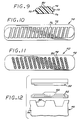
- the interconnect support 70 is illustrated in several views in Figures 8-11.
- the interconnect support 70 is preferably a single piece of a compliant elastomeric material such as silicone rubber, having a configuration suitable for applying pressure.
- the support 70 includes a central section 72 having a ridge 74 extending upwardly and a ridge 76 extending downwardly.
- Each of the ridges 74 and 76 is tapered slightly inwardly from its base on the central section 72 toward its flat top, for lateral rigidity and to permit extraction from a mold during fabrication.
- the ridges 74 and 76 are positioned to underlie the locations where the traces and/or pads are in facing register, and particularly to underlie the bumps 66. That is, since the pads in any group may be viewed as in a slanted pattern as indicated by the dashed line 78 in Figure 5, the ridges 74 and 76 are arranged to follow that same slanted pattern.
- the ridge 74 extends upwardly in the sense that it extends toward the contacting traces and pads, when the support 70 is placed below the traces and pads in the manner illustrated in Figures 8 and 12.
- a series of protrusions 80 extend further upwardly from the top of the ridge 74.
- One of the protrusions 80 is disposed under each of the registered pairs of traces, trace and pad, or pads and in particular under each of the bumps 66.
- the protrusions are slightly tapered inwardly from their bases on the ridge 74 toward their flat upper surface, for rigidity and producibility.
- the compound structure of upward and downward ridges and upward protrusions permits the manufacture of the support 70 in an elastomer molding operation, and also allows the protrusions to be relatively short.
- the protrusions 80 While in other situations an interconnect support might have only relatively long protrusions under the pads, in the present situation of closely spaced pads it is necessary that the protrusions 80 be relatively short in height. if the protrusions were significantly longer in relation to their widths, they would not have the necessary buckling resistance to support a substantial force and might buckle when the interconnect is made. The result would be an improperly distributed load and too low a pressure to achieve and maintain the interconnection. The short height of the protrusions 80 also permits the protrusions to be compressed when pressure is applied at the time the make/break connection is made.
- Figures 8 and 12 illustrate the preferred placement of the interconnect support 70, for a case where the traces both terminate in pads. Only one support 70 is used for each pair of pads 50 and 52 in the illustrated embodiment, but two supports could be used.
- the support 70 may be on either the printer 34 or the cartridge 10, but in the preferred approach is located on the printer side as part of the carriage 36.
- the interconnect support 70 sits on the shelf 48.
- the pad 52 of the trace 46 on the end of the cable 44 rests on top of the protrusion 80 of the support 70.
- the bump 66 is on the pad 52, on the printer side of the interconnect.
- the pad 50 is at the end of the trace 30 of the flexible interconnect circuit 32, which is supported by the manifold 22.
- the make/break interconnect is made by lowering the print head cartridge 10 into the pocket 42 on the carriage 36 of the printer 34, the respective pads 50 and 52 come into facing contact (with the bump 66 between them), and the make/break interconnection is made. At a later time, the cartridge 10 is removed from the printer 34, and the interconnection is broken.
- the interconnect support 70 helps to ensure that the interconnect is achieved with a maximum pressure possible from the available interconnect force.
- the approach of the invention provides an interconnect structure that permits a high density of electrical leads to extend to a device of small dimension, and for the interconnections to the external circuitry to be accomplished in a confined space.
- Improved bump and interconnect support structures are presented that permit connection to be accomplished quickly and reliably, and with the proper applied force. This approach permits the maximum misalignment tolerance in a minimum space, an important advantage for advanced printers requiring a high density of electrical interconnections.
Landscapes
- Ink Jet (AREA)
- Particle Formation And Scattering Control In Inkjet Printers (AREA)
- Accessory Devices And Overall Control Thereof (AREA)
Claims (8)
- Ein Gegenstand (10), der als Tintenstrahldruckerkomponente wirksam ist, der folgende Merkmale aufweist:
eine Einrichtung zum Ausstoßen von Färbemitteltröpfchen in Richtung eines Druckmediums, wobei die Einrichtung zum Ausstoßen eine Ausstoßeinrichtung (12) einschließt; und
mindestens eine Gruppe (54) von koplanaren, parallelen Leiterspuren (30), die sich von der Ausstoßvorrichtung (12) in Richtung eines Verbindungsortes erstrecken, wobei jede der Spuren (30) in der Gruppe (54) an ihrem Ende eine planare Kontaktanschlußstelle (50) hat, deren laterale Erstreckung größer ist als die Entfernung zwischen den Spuren (30) in der Gruppe (54), wobei die Anschlußstellen (50) in ihren Entfernungen von der Ausstoßvorrichtung (12) versetzt sind, so daß es Raum für die Anordnung aller Anschlußstellen (50) in der Ebene der Spuren (30) gibt. - Ein Gegenstand gemäß Anspruch 1, bei dem mindestens einige der Kontaktanschlußstellen (50) einen erhöhten Kontakthöcker (66) aus Metall einschließen, der auf mindestens eine Front der Kontaktanschlußstelle (50) abgeschieden ist.
- Ein Gegenstand gemäß Anspruch 1, bei dem mindestens einige der Kontaktanschlußstellen (50) folgende Merkmale einschließen:
eine Schicht (60) aus elektrisch nicht-leitfähigem Material auf einer Stirnfläche der Kontaktanschlußstellen (50),
eine Öffnung (64) durch das nicht-leitfähige Material auf jeder Kontaktanschlußstelle, und
einen metallischen Kontakthöcker (66), der auf jeder Kontaktanschlußfläche (50) durch die Öffnung (64) abgeschieden ist. - Ein Gegenstand gemäß irgendeinem der Ansprüche 1 bis 3, bei dem der Gegenstand mindestens zwei geometrisch ähnliche Gruppen (54) von koplanaren, parallelen Leiterspuren (30) umfaßt.
- Ein Gegenstand gemäß irgendeinem der Ansprüche 1 bis 4, der ferner folgende Merkmale aufweist:
ein nachgiebiges Verbindungseinrichtungstragebauteil (70), das unter den Kontaktanschlußstellen (50) angeordnet ist, wobei das Verbindungseinrichtungstragebauteil (70) folgende Merkmale aufweist:
eine Reihe von Rippen (74) auf einer Seite des Tragebauteils (70), die unterhalb der Kontaktanschlußstellen (50) liegen;
eine zweite Reihe von Rippen (76) auf der anderen Seite des Tragebauteils, die unterhalb der Kontaktanschlußstellen (50) liegen; und
eine Reihe von Vorsprüngen (80) auf der Rippe (74), die den Kontaktanschlußstellen (50) gegenüberliegt, wobei die Vorsprünge (80) sich in Richtung der Anschlußstellen (50) erstrecken. - Ein Gegenstand gemäß Anspruch 1, bei dem mindestens einige der Kontaktanschlußstellen (50) angepaßt sind, um entsprechende Kontaktanschlußstellen mit einem darauf abgeschiedenen erhöhten Kontakthöcker in gegenüberliegender Beziehung mit den Kontaktanschlußstellen des Gegenstands aufzunehmen.
- Ein Gegenstand gemäß Anspruch 1, bei dem mindestens einige der Kontaktanschlußstellen (50) angepaßt sind, um entsprechende Kontaktanschlußstellen aufzunehmen, wobei die entsprechenden Kontaktanschlußstellen eine Schicht aus elektrisch nicht-leitendem Material auf einer Stirnfläche der Kontaktanschlußstellen, eine Öffnung durch das nicht-leitfähige Material auf jeder Kontaktanschlußstelle und einen metallischen Kontakthöcker einschließen, der auf jeder Kontaktansschlußstelle durch die Öffnung abgeschieden ist.
- Ein Gegenstand gemäß Anspruch 1, bei dem mindestens einige der Kontaktanschlußstellen angepaßt sind, um entsprechende Kontaktanschlußstellen aufzunehmen, wobei die entsprechenden Kontaktanschlußstellen ferner ein nachgiebiges Verbindungseinrichtungstragebauteil, das unterhalb der Kontaktanschlußstellen angeordnet ist, aufweisen, wobei das Verbindungseinrichtungstragebau teil eine erste Reihe von Rippen auf einer Seite des Tragebauteils und unter den Kontaktanschlußstellen liegend, eine zweite Reihe von Rippen auf der anderen Seite des Tragebauteils und unter den Kontaktanschlußstellen liegend und eine Reihe von Vorsprüngen auf der Rippe, die den Kontaktanschlußstellen gegenüberliegt, einschließt.
Applications Claiming Priority (2)
| Application Number | Priority Date | Filing Date | Title |
|---|---|---|---|
| US07/385,615 US4940413A (en) | 1989-07-26 | 1989-07-26 | Electrical make/break interconnect having high trace density |
| US385615 | 1989-07-26 |
Publications (2)
| Publication Number | Publication Date |
|---|---|
| EP0410656A1 EP0410656A1 (de) | 1991-01-30 |
| EP0410656B1 true EP0410656B1 (de) | 1994-06-22 |
Family
ID=23522156
Family Applications (1)
| Application Number | Title | Priority Date | Filing Date |
|---|---|---|---|
| EP90307986A Expired - Lifetime EP0410656B1 (de) | 1989-07-26 | 1990-07-20 | Elektrisch lösbare Verbindung mit hoher Kontaktdichte |
Country Status (5)
| Country | Link |
|---|---|
| US (1) | US4940413A (de) |
| EP (1) | EP0410656B1 (de) |
| JP (1) | JP3142281B2 (de) |
| CA (1) | CA2008181A1 (de) |
| DE (1) | DE69010101T2 (de) |
Families Citing this family (24)
| Publication number | Priority date | Publication date | Assignee | Title |
|---|---|---|---|---|
| US5123852A (en) * | 1991-05-17 | 1992-06-23 | International Business Machines Corporation | Modular electrical connector |
| US5568171A (en) * | 1992-04-02 | 1996-10-22 | Hewlett-Packard Company | Compact inkjet substrate with a minimal number of circuit interconnects located at the end thereof |
| US5411343A (en) * | 1992-07-31 | 1995-05-02 | Hewlett-Packard Company | Redundant make/break interconnect for a print head |
| CA2112182C (en) * | 1992-12-25 | 2000-06-27 | Masami Ikeda | Detachable ink jet unit and ink jet apparatus |
| IT1272050B (it) * | 1993-11-10 | 1997-06-11 | Olivetti Canon Ind Spa | Dispositivo stampante parallelo con struttura modulare e relativo procedimento di realizzazione. |
| US5565900A (en) * | 1994-02-04 | 1996-10-15 | Hewlett-Packard Company | Unit print head assembly for ink-jet printing |
| US6305786B1 (en) | 1994-02-23 | 2001-10-23 | Hewlett-Packard Company | Unit print head assembly for an ink-jet printer |
| US6536871B1 (en) | 1997-11-05 | 2003-03-25 | Hewlett-Packard Company | Reliable flex circuit interconnect on inkjet print cartridge |
| US6188414B1 (en) | 1998-04-30 | 2001-02-13 | Hewlett-Packard Company | Inkjet printhead with preformed substrate |
| US6328423B1 (en) | 1999-08-16 | 2001-12-11 | Hewlett-Packard Company | Ink jet cartridge with integrated circuitry |
| US6454955B1 (en) | 1999-10-29 | 2002-09-24 | Hewlett-Packard Company | Electrical interconnect for an inkjet die |
| EP1095773B1 (de) | 1999-10-29 | 2003-07-09 | Hewlett-Packard Company, A Delaware Corporation | Tintenstrahldruckkopf mit verbesserter Zuverlässigkeit |
| JP4533522B2 (ja) * | 1999-10-29 | 2010-09-01 | ヒューレット・パッカード・カンパニー | インクジェットのダイ用の電気的相互接続 |
| US6508674B1 (en) | 2000-10-18 | 2003-01-21 | Storage Technology Corporation | Multi-layer conductive device interconnection |
| US6699395B1 (en) | 2000-10-18 | 2004-03-02 | Storage Technology Corporation | Method of forming alignment features for conductive devices |
| US6431876B1 (en) | 2000-10-18 | 2002-08-13 | Storage Technology Corporation | Conductive trace interconnection |
| US6641408B1 (en) | 2000-10-18 | 2003-11-04 | Storage Technology Corporation | Compliant contacts for conductive devices |
| US6799833B2 (en) * | 2000-12-28 | 2004-10-05 | Canon Kabushiki Kaisha | Ink jet recording head and ink jet recording apparatus |
| US20050096554A1 (en) * | 2002-11-27 | 2005-05-05 | Dudik Evan M. | Acoustic medical sensor for ultrasound imaging |
| WO2004049913A2 (en) * | 2002-11-27 | 2004-06-17 | Black Toe Medical Iii, Inc. | Immersible ultrasound probe and cable |
| US7025440B2 (en) * | 2003-10-15 | 2006-04-11 | Lexmark International, Inc. | Low profile ink jet cartridge assembly |
| GB2413306A (en) * | 2004-04-23 | 2005-10-26 | Hewlett Packard Development Co | Ink cartridge having terminals and conductive tracks applied directly thereon. |
| US20080306387A1 (en) | 2007-04-13 | 2008-12-11 | Schutz Ronald W | Finger mounted imaging and sensing assembly |
| US20120208380A1 (en) * | 2011-02-16 | 2012-08-16 | International Business Machines Corporation | Contact reliability in separable electrical interfaces |
Family Cites Families (9)
| Publication number | Priority date | Publication date | Assignee | Title |
|---|---|---|---|---|
| US3716907A (en) * | 1970-11-20 | 1973-02-20 | Harris Intertype Corp | Method of fabrication of semiconductor device package |
| US4125310A (en) * | 1975-12-01 | 1978-11-14 | Hughes Aircraft Co | Electrical connector assembly utilizing wafers for connecting electrical cables |
| US4179802A (en) * | 1978-03-27 | 1979-12-25 | International Business Machines Corporation | Studded chip attachment process |
| JPS59194860A (ja) * | 1983-04-19 | 1984-11-05 | Canon Inc | 液体噴射記録ヘツド |
| US4635080A (en) * | 1984-03-30 | 1987-01-06 | Canon Kabushiki Kaisha | Liquid injection recording apparatus |
| US4602317A (en) * | 1984-12-13 | 1986-07-22 | Gte Communication Systems Corporation | Printed wiring board connector |
| US4635073A (en) * | 1985-11-22 | 1987-01-06 | Hewlett Packard Company | Replaceable thermal ink jet component and thermosonic beam bonding process for fabricating same |
| US4806106A (en) * | 1987-04-09 | 1989-02-21 | Hewlett-Packard Company | Interconnect lead frame for thermal ink jet printhead and methods of manufacture |
| US4791440A (en) * | 1987-05-01 | 1988-12-13 | International Business Machine Corporation | Thermal drop-on-demand ink jet print head |
-
1989
- 1989-07-26 US US07/385,615 patent/US4940413A/en not_active Expired - Lifetime
-
1990
- 1990-01-19 CA CA002008181A patent/CA2008181A1/en not_active Abandoned
- 1990-07-20 EP EP90307986A patent/EP0410656B1/de not_active Expired - Lifetime
- 1990-07-20 DE DE69010101T patent/DE69010101T2/de not_active Expired - Lifetime
- 1990-07-25 JP JP02198975A patent/JP3142281B2/ja not_active Expired - Lifetime
Also Published As
| Publication number | Publication date |
|---|---|
| DE69010101T2 (de) | 1994-10-13 |
| US4940413A (en) | 1990-07-10 |
| EP0410656A1 (de) | 1991-01-30 |
| JPH0365347A (ja) | 1991-03-20 |
| CA2008181A1 (en) | 1991-01-26 |
| JP3142281B2 (ja) | 2001-03-07 |
| DE69010101D1 (de) | 1994-07-28 |
Similar Documents
| Publication | Publication Date | Title |
|---|---|---|
| EP0410656B1 (de) | Elektrisch lösbare Verbindung mit hoher Kontaktdichte | |
| US5411343A (en) | Redundant make/break interconnect for a print head | |
| EP0654958B1 (de) | TAB-Schaltungsschmelzverbindungen zur Trennung oder Kodierungsinformation | |
| US6350013B1 (en) | Carrier positioning for wide-array inkjet printhead assembly | |
| US5706040A (en) | Reliable contact pad arrangement on plastic print cartridge | |
| US6341845B1 (en) | Electrical connection for wide-array inkjet printhead assembly with hybrid carrier for printhead dies | |
| EP0240710B1 (de) | Verbindung mit nahezu linearer Federcharakteristik für elastich verbundene Schaltungsanordnungen | |
| EP0616395B1 (de) | Verfahren und Vorrichtung für die Herstellung von elektrisch zusammengeschalteten Schaltungen | |
| US6250738B1 (en) | Inkjet printing apparatus with ink manifold | |
| JP3477241B2 (ja) | 印刷ヘッドの製造方法および印刷ヘッド | |
| EP0289347A2 (de) | Wärme-Tintenstrahldruckkopf | |
| JPH0722144A (ja) | 電気的相互接続回路の生成方法及びシステム | |
| JPH02151445A (ja) | 改良されたサーマルインク印刷カートリッジ組立体 | |
| CN100532105C (zh) | 挠性打印头电路 | |
| EP1243419B1 (de) | Elektrische Verbindung für zeilenbreite Tintenstrahldruckkopfanordnung | |
| JP3432503B2 (ja) | 内部電気経路指定システムを備えるワイド・アレイ・インクジェット印字ヘッド・アセンブリ | |
| US6464333B1 (en) | Inkjet printhead assembly with hybrid carrier for printhead dies | |
| JP2002321352A (ja) | インクジェットプリントヘッド・アセンブリおよびその形成方法ならびにインクジェットプリントヘッド・アセンブリ用の複合キャリア | |
| JP2004148816A (ja) | エッジ封止基板と、エッジ封止基板を得る方法 | |
| CN100446978C (zh) | 软性印刷电路板的结构 | |
| JPH08244245A (ja) | プリント装置 | |
| US5992976A (en) | Ink-jet printhead | |
| JP2003072042A (ja) | インクジェット記録ヘッドおよびインクジェット記録装置 | |
| JP2000079687A (ja) | 記録ヘッド及び該ヘッドを有する記録装置 | |
| JPH10230603A (ja) | インクジェット記録ヘッドおよびその組立方法ならびにそのヘッドを用いたインクジェット記録装置 |
Legal Events
| Date | Code | Title | Description |
|---|---|---|---|
| PUAI | Public reference made under article 153(3) epc to a published international application that has entered the european phase |
Free format text: ORIGINAL CODE: 0009012 |
|
| AK | Designated contracting states |
Kind code of ref document: A1 Designated state(s): DE FR GB IT NL |
|
| 17P | Request for examination filed |
Effective date: 19910408 |
|
| 17Q | First examination report despatched |
Effective date: 19930112 |
|
| GRAA | (expected) grant |
Free format text: ORIGINAL CODE: 0009210 |
|
| AK | Designated contracting states |
Kind code of ref document: B1 Designated state(s): DE FR GB IT NL |
|
| REF | Corresponds to: |
Ref document number: 69010101 Country of ref document: DE Date of ref document: 19940728 |
|
| ET | Fr: translation filed | ||
| ITF | It: translation for a ep patent filed | ||
| PLBE | No opposition filed within time limit |
Free format text: ORIGINAL CODE: 0009261 |
|
| STAA | Information on the status of an ep patent application or granted ep patent |
Free format text: STATUS: NO OPPOSITION FILED WITHIN TIME LIMIT |
|
| 26N | No opposition filed | ||
| NLS | Nl: assignments of ep-patents |
Owner name: HEWLETT-PACKARD COMPANY (A DELAWARE CORPORATION) |
|
| REG | Reference to a national code |
Ref country code: GB Ref legal event code: 732E |
|
| REG | Reference to a national code |
Ref country code: FR Ref legal event code: TP |
|
| REG | Reference to a national code |
Ref country code: GB Ref legal event code: IF02 |
|
| PGFP | Annual fee paid to national office [announced via postgrant information from national office to epo] |
Ref country code: FR Payment date: 20090717 Year of fee payment: 20 |
|
| PGFP | Annual fee paid to national office [announced via postgrant information from national office to epo] |
Ref country code: GB Payment date: 20090727 Year of fee payment: 20 Ref country code: NL Payment date: 20090724 Year of fee payment: 20 Ref country code: DE Payment date: 20090729 Year of fee payment: 20 |
|
| PGFP | Annual fee paid to national office [announced via postgrant information from national office to epo] |
Ref country code: IT Payment date: 20090729 Year of fee payment: 20 |
|
| REG | Reference to a national code |
Ref country code: NL Ref legal event code: V4 Effective date: 20100720 |
|
| REG | Reference to a national code |
Ref country code: GB Ref legal event code: PE20 Expiry date: 20100719 |
|
| PG25 | Lapsed in a contracting state [announced via postgrant information from national office to epo] |
Ref country code: NL Free format text: LAPSE BECAUSE OF EXPIRATION OF PROTECTION Effective date: 20100720 |
|
| PG25 | Lapsed in a contracting state [announced via postgrant information from national office to epo] |
Ref country code: GB Free format text: LAPSE BECAUSE OF EXPIRATION OF PROTECTION Effective date: 20100719 |
|
| PG25 | Lapsed in a contracting state [announced via postgrant information from national office to epo] |
Ref country code: DE Free format text: LAPSE BECAUSE OF EXPIRATION OF PROTECTION Effective date: 20100720 |