EP0411325B1 - Gebrauch eines LCD's in einer Kopiervorrichtung und Methode - Google Patents
Gebrauch eines LCD's in einer Kopiervorrichtung und Methode Download PDFInfo
- Publication number
- EP0411325B1 EP0411325B1 EP90112491A EP90112491A EP0411325B1 EP 0411325 B1 EP0411325 B1 EP 0411325B1 EP 90112491 A EP90112491 A EP 90112491A EP 90112491 A EP90112491 A EP 90112491A EP 0411325 B1 EP0411325 B1 EP 0411325B1
- Authority
- EP
- European Patent Office
- Prior art keywords
- modulator array
- radiation
- lcd modulator
- pixels
- image
- Prior art date
- Legal status (The legal status is an assumption and is not a legal conclusion. Google has not performed a legal analysis and makes no representation as to the accuracy of the status listed.)
- Expired - Lifetime
Links
- 238000000034 method Methods 0.000 title claims abstract description 17
- 230000005855 radiation Effects 0.000 claims abstract description 107
- 230000004044 response Effects 0.000 claims description 25
- 239000004973 liquid crystal related substance Substances 0.000 claims description 6
- 230000000903 blocking effect Effects 0.000 claims 1
- 230000001678 irradiating effect Effects 0.000 claims 1
- 238000003491 array Methods 0.000 description 9
- 239000005337 ground glass Substances 0.000 description 5
- 238000005259 measurement Methods 0.000 description 5
- 206010073306 Exposure to radiation Diseases 0.000 description 4
- 238000005286 illumination Methods 0.000 description 4
- 239000000463 material Substances 0.000 description 4
- 230000001427 coherent effect Effects 0.000 description 3
- 238000011161 development Methods 0.000 description 3
- 230000018109 developmental process Effects 0.000 description 3
- XKRFYHLGVUSROY-UHFFFAOYSA-N Argon Chemical compound [Ar] XKRFYHLGVUSROY-UHFFFAOYSA-N 0.000 description 2
- 230000005540 biological transmission Effects 0.000 description 2
- 239000003086 colorant Substances 0.000 description 2
- 238000012937 correction Methods 0.000 description 2
- 230000000694 effects Effects 0.000 description 2
- 230000003287 optical effect Effects 0.000 description 2
- 230000010287 polarization Effects 0.000 description 2
- 238000012545 processing Methods 0.000 description 2
- 238000002834 transmittance Methods 0.000 description 2
- OAICVXFJPJFONN-UHFFFAOYSA-N Phosphorus Chemical compound [P] OAICVXFJPJFONN-UHFFFAOYSA-N 0.000 description 1
- 230000009471 action Effects 0.000 description 1
- 238000007792 addition Methods 0.000 description 1
- 239000000654 additive Substances 0.000 description 1
- 230000000996 additive effect Effects 0.000 description 1
- 229910052786 argon Inorganic materials 0.000 description 1
- UIZLQMLDSWKZGC-UHFFFAOYSA-N cadmium helium Chemical compound [He].[Cd] UIZLQMLDSWKZGC-UHFFFAOYSA-N 0.000 description 1
- 230000006835 compression Effects 0.000 description 1
- 238000007906 compression Methods 0.000 description 1
- 238000002508 contact lithography Methods 0.000 description 1
- 238000012217 deletion Methods 0.000 description 1
- 230000037430 deletion Effects 0.000 description 1
- 238000010790 dilution Methods 0.000 description 1
- 239000012895 dilution Substances 0.000 description 1
- 238000009826 distribution Methods 0.000 description 1
- 239000005338 frosted glass Substances 0.000 description 1
- CPBQJMYROZQQJC-UHFFFAOYSA-N helium neon Chemical compound [He].[Ne] CPBQJMYROZQQJC-UHFFFAOYSA-N 0.000 description 1
- 238000003384 imaging method Methods 0.000 description 1
- 239000000203 mixture Substances 0.000 description 1
- 238000012986 modification Methods 0.000 description 1
- 230000004048 modification Effects 0.000 description 1
- 238000009828 non-uniform distribution Methods 0.000 description 1
- 230000008520 organization Effects 0.000 description 1
- 230000000630 rising effect Effects 0.000 description 1
- 238000005070 sampling Methods 0.000 description 1
- 230000003595 spectral effect Effects 0.000 description 1
Images


Classifications
-
- H—ELECTRICITY
- H04—ELECTRIC COMMUNICATION TECHNIQUE
- H04N—PICTORIAL COMMUNICATION, e.g. TELEVISION
- H04N1/00—Scanning, transmission or reproduction of documents or the like, e.g. facsimile transmission; Details thereof
- H04N1/40—Picture signal circuits
- H04N1/40025—Circuits exciting or modulating particular heads for reproducing continuous tone value scales
- H04N1/4005—Circuits exciting or modulating particular heads for reproducing continuous tone value scales with regulating circuits, e.g. dependent upon ambient temperature or feedback control
-
- H—ELECTRICITY
- H04—ELECTRIC COMMUNICATION TECHNIQUE
- H04N—PICTORIAL COMMUNICATION, e.g. TELEVISION
- H04N1/00—Scanning, transmission or reproduction of documents or the like, e.g. facsimile transmission; Details thereof
- H04N1/40—Picture signal circuits
- H04N1/40025—Circuits exciting or modulating particular heads for reproducing continuous tone value scales
- H04N1/40031—Circuits exciting or modulating particular heads for reproducing continuous tone value scales for a plurality of reproducing elements simultaneously
-
- H—ELECTRICITY
- H04—ELECTRIC COMMUNICATION TECHNIQUE
- H04N—PICTORIAL COMMUNICATION, e.g. TELEVISION
- H04N1/00—Scanning, transmission or reproduction of documents or the like, e.g. facsimile transmission; Details thereof
- H04N1/46—Colour picture communication systems
- H04N1/50—Picture reproducers
- H04N1/502—Reproducing the colour component signals dot-sequentially or simultaneously in a single or in adjacent picture-element positions
Definitions
- the present invention pertains to methods and apparatus which utilize an LCD modulator array for printing and/or enlarging an image recorded in a color film negative, a positive transparency, a color print or electronically.
- a full color printer and/or enlarger which utilizes an LCD modulator array for printing and/or enlarging an image recorded in a color film negative a positive transparency or a color print must scan the color film negative a number of times to acquire information about the images' chrominance and density. For example, once for each of three colors, to obtain a density value which is associated with each pixel (picture element) of the LCD modulator array.
- the scan time required to perform each scan can be quite long because of the response times of typical liquid crystal materials used in LCD modulator arrays. For example, FIG. 1 shows a response time curve for a typical LCD material.
- the "opening time" of a pixel in the LCD modulator array i.e., the time it takes for the pixel in the LCD modulator array to convert from a state where less than or equal to about 1% of the radiation incident thereupon is transmitted to a state where over 90% of the radiation incident thereupon is transmitted
- the "closing time" of the pixel in the LCD modulator array i.e., the time it takes for the pixel in the LCD modulator array to convert from a state where over 90% of the radiation incident thereupon is transmitted to a state where less than or equal to about 1% of the radiation incident thereupon is transmitted, is typically about 20 ms. to 30 ms.
- the total opening time for the pixels of the LCD modulator array during each scan would be approximately 4 seconds and the total closing time for the pixels during each scan could be several minutes.
- a typical LCD modulator array utilized in a mode in which each pixel is opened and closed before the next succeeding pixel is opened and closed during each scan results in an extremely slow printer and/or enlarger.
- Another additional problem associated with the use of an LCD modulator array for printing and/or enlarging an image recorded in, for example, a color film negative occurs because the pixels in an LCD modulator array are not completely opaque, even when completely closed.
- an opacity problem occurs when an LCD modulator array is utilized for printing and/or enlarging. This opacity problem can be understood by considering a typical case where a closed pixel leaks about 1% of the radiation incident thereupon.
- a copying machine in accordance with the preamble of claim 1 is known from US-A-4239385. From this document it is known to scan the transparent original being copied on a pointwise, linewise or zonewise basis, and to derive from such scanning operation information concerning density and/or color which is then used to control the operation of the exposure system of the copying machine, either automatically or with the intermediary of operator participation.
- the corrective expedients then employed include proper selection of the intensity or duration of the exposure radiation, the use of color filters for establishing a proper spectral composition or balance for the exposure radiation in accordance with subtractive or additive copying procedures, and so forth.
- the correction is obtained by utilizing, in the light path which extends from the light source through the transparent original onto the photosensitive printing medium, an intermediate light-transmission control structure comprised of a multitude of tiny zones whise light transmittances can be individually varied.
- a control electronics preferably incorporating a computer and multiplexer, controls the transmissivity values of the multitude of controllable-transmissivity elements of the array.
- the array is employed to establish a two-dimensional controllably non-uniform distribution of exposure radiation onto the photosensitive medium. This is done to implement non-uniform density and/or color correction during printing, or to superimpose onto the image projected onto the photosensitive medium images of symbols, text or the like, which are to be appear on the final copy.
- Claims 2 through 6 are directed to further embodiments and developments of the apparatus of claim 1 whereas claim 7 is directed to a printer using the apparatus of claim 1 for determine exposure levels in order to print an image improved relative to the original in the manner as discussed above.
- Embodiments of the present invention comprise method and apparatus which utilize an LCD modulator array for printing and/or enlarging an image recorded in a color film negative; a positive transparency, or a color print, which method and apparatus: (a) operate rapidly; (b) utilize an LCD modulator array which is comprised of pixels whose closing time plus opening time is approximately 30 milliseconds; and (c) achieve a modulation ratio of 10:1 (adequate for dodging applications) to 100:1 (adequate for printing a photograph from electronically stored information).
- each pixel of the LCD modulator array is opened and closed in a rapid sequence, one after the other, at intervals which are much shorter than the closing time of the pixels of the LCD modulator array.
- the amount of radiation transmitted by each opened pixel of the LCD modulator array is determined by detecting a spike of radiation which is transmitted through the rapidly opened pixel and by detecting and subtracting a background amount produced by radiation which is transmitted through other, slowly closing pixels.
- a photosensor exposed to radiation transmitted by the LCD modulator array will provide a rapidly rising response when a pixel is opened and (b) the photosensor response will decay gradually, in accordance with the curve shown in FIG. 1 and the local density of, for example, the color film negative, when the pixel is subsequently closed.
- the tail-end information of the decaying photosensor response is unnecessary, and it is truncated by opening the next pixel in a sequence of pixels in the LCD modulator array to generate another rise in the photosensor response.
- a savings in time for a full scan may readily be a factor of 10 or 100.
- the pixels of the LCD modulator array are opened and closed in response to signals provided by a controller means, and the radiation transmitted through the LCD modulator array and, for example, the color film negative, is detected by photosensor means.
- the controller converts the response from the photosensor means which is exposed to radiation transmitted by the LCD modulator array into: (a) a "background” sample of the radiation transmitted by the LCD modulator array before the controller sent a signal to cause a particular pixel in the LCD modulator array to be opened and (b) a "spike” sample of the radiation transmitted by the LCD modulator array after the controller sent a signal to cause the particular pixel to be opened.
- the controller determines a measure of the amount of radiation transmitted by the particular pixel to be the difference between the "spike” sample corresponding to the level of the radiation received by the photosensor after the particular pixel was opened and the "background” sample corresponding to the level of radiation received by the photosensor before the particular pixel was opened.
- This amount of radiation is the amount of radiation which impinges upon the color film negative as a result of opening the particular pixel.
- the controller then examines the response from the photosensor means which is disposed to detect radiation transmitted by the color film negative. The controller converts this response into a "film” sample of the radiation transmitted by the color film negative at the time the "spike” sample is taken, i.e., after the particular pixel was opened.
- the "film” samples of radiation transmitted by the color film negative are stored for later use during printing and/or enlarging.
- the inventive method and apparatus which utilizes an LCD modulator array for printing and/or enlarging an image recorded in, for example, a color film negative operates as follows. All the pixels in the LCD modulator array are opened at once and each one is closed by a controller, when it has produced the required exposure appropriate for its local area of the color film negative.
- LCD modulator arrays which are comprised of pixels having a small closing time and a relatively long opening time may be utilized to provide embodiments of the present invention in a manner which is analogous to the above-described embodiments.
- LCD modulator arrays may be fabricated by rotating the direction of polarization of polarizers which comprise the LCD modulator arrays.
- FIG. 2 shows an embodiment of an apparatus for determining appropriate radiation exposures for printing and/or enlarging an image recorded in color film negative 100 in accordance with the present invention.
- LCD modulator array 400 is comprised of liquid crystal pixels which can be opened to transmit radiation and closed to block radiation. As will be explained in detail below, the pixels of LCD modulator array 400 are sequentially opened and closed at a rapid rate, i.e., at intervals which are much shorter than the closing time of the pixels of the LCD modulator array.
- the radiation in each beam which is transmitted by the pixels of LCD modulator array 400 and by color film negative 100 is measured, and the measurements are stored by controller 310.
- Controller 310 determines the relative contributions of red, green and blue radiation in the original exposure which produced the image recorded in each area of color film negative 100 which is sequentially illuminated by each beam. Controller 310 makes this determination by comparing the measurements of red, green and blue radiation which were transmitted through each area of color film negative 100 after passing through LCD modulator array 400. These relative contributions of red, green, and blue radiation in the original exposure are used, in a manner which is well known to those of ordinary skill in the art, to calculate appropriate pixel exposure times for LCD modulator array 400 for the red, green, and blue radiation so that illumination of color film negative 100 through LCD modulator array 400 will produce the appropriate color exposure of a copy film.
- apparatus 200 is comprised of three coherent laser radiation sources 212, 214, and 216.
- Laser radiation source 212 comprises a helium-cadmium laser for providing a beam of blue radiation
- laser radiation source 214 comprises an argon laser for providing a beam of green radiation
- laser radiation source 216 comprises a helium-neon laser for providing a beam of red radiation.
- Blue laser radiation from laser source 212 passes through dichroic mirror 226, through dichroic mirror 230 and aperture 234.
- Green laser radiation from laser source 214 is directed to dichroic mirror 226 by reflecting surface 228.
- Dichroic mirror 226 directs the green laser radiation to dichroic mirror 230 and thence to aperture 234.
- Red laser radiation from laser source 216 is directed to dichroic mirror 230 by reflecting surface 232 and then to aperture 234.
- Laser sources 212, 214 and 216 are energized in succession, in response to signals from controller 310, and the laser radiation from each is directed through aperture 234 which blocks unwanted diffracted orders. After passing through aperture 234, the laser radiation from laser sources 212, 214, and 216, respectively, is reflected from reflecting surfaces 236 and 610 and is then transmitted through ground or frosted glass 244 which is rotatably driven about axis AA by motor 246. Ground glass 244 changes the laser radiation from coherent radiation to incoherent radiation to eliminate any speckle effect which is normally associated with coherent laser radiation.
- the spot of radiation projected onto ground glass 244 is thereafter broadened by non-achromatic negative lens 611 and, together with thin, non-achromatic, positive field lens 612, provides a beam which encompasses LCD modulator array 400.
- a first portion of the radiation transmitted by LCD modulator array 400 is deflected by beamsplitter 520 and focused by positive lens 525 onto red, blue and green photosensors 530, 531, and 532, respectively, and a second portion of the radiation transmitted by LCD modulator array 400 is projected upon color film negative 100 by copy lens 615 and thin, non-achromatic, positive field lens 613.
- An enlarging lens may be used in place of copy lens 615 if an enlargement of the image recorded in color film negative 100 is being made.
- the radiation transmitted by color film negative 100 is focused by positive print lens 614 onto red, green, and blue color photosensors 550, 551, and 552, respectively.
- photosensors 530-532 and photosensors 550-552 ought to be so close together, respectively, that the photosensors in each group individually respond uniformly to information anywhere in LCD modulator array 400 and color film negative 100, respectively.
- the pixels of LCD modulator array 400 are opened and closed in a rapid sequence in response to signals provided by controller 310, one after the other, at intervals which are much shorter than the closing time of the pixels of the LCD modulator array.
- Each trio of photosensors i.e., photosensors 530, 531, and 532 and photosensors 550, 551, and 552, provides analog electronic information signals corresponding to the intensity of the particular color radiation transmitted thereto.
- the electronic information signals output from each trio of photosensors are amplified by amplifiers in controller 310 (not shown) in a manner which is well known to those of ordinary skill in the art and, thereafter, they are converted from analog signals to digital signals by analog-to-digital converters in controller 310 (not shown) in a manner which is also well known to those of ordinary skill in the art.
- Controller 310 converts the response from photosensors 530, 531, and 532 into: (a) a "background” sample of the radiation transmitted by LCD modulator array 400 before controller 310 sent a signal to LCD modulator array 400 to cause a particular pixel thereof to be opened and (b) a "spike” sample of the radiation transmitted by LCD modulator array 400 after controller 310 sent a signal to LCD modulator array 400 to cause the particular pixel to be opened.
- Controller 310 determines a measure of the amount of radiation transmitted by the particular pixel to be the difference between the "spike” sample corresponding to the level of the radiation received by photosensors 530, 531, and 532 after the particular pixel was opened and the "background” sample corresponding to the level of radiation received by photosensors 530, 531, and 532 before the particular pixel was opened.
- This amount of radiation is the amount of radiation which impinges upon color film negative 100 as a result of opening the particular pixel. Note that the specific times at which the "spike” sample and the "background” sample are taken for a particular type of LCD material are determined in accordance with methods well-known to those of ordinary skill in the art.
- controller 310 converts the response from photosensors 550, 551, and 552 into a "film” sample at the time the "spike” sample is taken, i.e., after the particular pixel was opened.
- the "film” sample is the radiation transmitted by color film negative 100 when the particular pixel was open.
- Controller 310 stores the "film” samples of radiation transmitted through color film negative 100 for later use during printing and/or enlarging.
- controller 310 sends signals to LCD modulator array 400 to cause each pixel thereof to be opened and closed in a rapid sequence, one after another, at intervals which are much shorter than the closing time of the pixels.
- FIG. 1 the transmittance of a pixel which is closed after being opened decays slowly and, as a result, the response of a photodetector, such as photodetector 530, 531, or 532 of FIG. 2, is roughly as shown in FIG. 4.
- a photodetector such as photodetector 530, 531, or 532 of FIG.
- This information is used, in accordance with the present invention, when controller 310 converts the response of photodetectors 530, 531, and 532 into samples at two sample windows, which sample windows are shown for illustrative purposes in FIG. 5.
- the first sample, "background” sample 700 is taken before controller 310 sent a signal to LCD modulator array 400 to cause it to open a particular pixel. This occurs at a predetermined time after controller 310 sent a signal to LCD modulator array 400 to cause it to close the pixel which had previously been opened in the sequence.
- “Background” sample 700 provides an indication of the background radiation transmitted by LCD modulator array 400.
- the second sample, "spike” sample 710 is taken after controller 310 sent a signal to LCD modulator array 400 to cause it to open the particular pixel. Due to the fast opening time of the pixel, as indicated by FIG. 1, "spike" sample 710 provides an indication of the radiation transmitted by the particular pixel.
- controller 310 determines the relative contributions of red, green and blue radiation in the original color exposure which produced the image recorded in each area of color film negative 100 which is sequentially illuminated by each beam. Controller 310 makes this determination by comparing the measurements of the red, green and blue radiation which were transmitted through each area of color film negative 100 after passing through LCD modulator array 400. These relative contributions of red, green, and blue radiation in the original exposure are used, in a manner which is well known to those of ordinary skill in the art, to calculate appropriate pixel exposure times for LCD modulator array 400 for the red, green, and blue radiation so that illumination of color film negative 100 through LCD modulator array 400 will produce the appropriate color exposure of copy film 300.
- picture quality enhancement by means of methods well known to those of ordinary skill in the art, such as, for example, dodging, may be used to determine appropriate amounts of radiation for transmission through the various pixels of LCD modulator array 400 to produce predetermined enhancements.
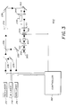
- FIG. 3 there is shown generally at 600 an embodiment of an apparatus for printing and/or enlarging an image recorded in color film negative 100, which embodiment uses radiation exposures determined and stored by controller 310 of apparatus 200 shown in FIG. 2.
- controller 310 of apparatus 200 shown in FIG. 2.
- the pixels comprising LCD modulator array 400 are all opened. Then, in succession, radiation from each of the three laser sources impinges upon and is transmitted through LCD modulator array 400 and color film negative 100 to strike color film 300. For each of the beams of radiation, the pixels of LCD modulator array 400 are closed at predetermined times, under the control of controller 310, in accordance with the measurements and calculations made as a result of using apparatus 200 shown in FIG. 2, to ensure that the exposure of color film 300 is substantially the same as that which produced the image recorded in color film negative 100.
- apparatus 200 and 600 which are denoted by the same numbers are the same, and they operate in the manner described above in regard to apparatus 200, except for certain additional features of controller 310.
- Laser sources 212, 214 and 216 are energized in succession, in response to signals from controller 310, and the laser radiation from each is directed through aperture 234 in the manner described above with regard to apparatus 200 shown in FIG. 2. After passing through aperture 234, the laser radiation from laser sources 212, 214, and 216, respectively, is reflected from reflecting surfaces 236 and 610 for transmission through ground glass 244.
- the spot of radiation projected onto ground glass 244 is thereafter broadened by non-achromatic negative lens 611 and, together with thin, non-achromatic, positive field lens 612, provides a beam which encompasses LCD array modulator array 400.
- the radiation transmitted by LCD modulator array 400 is projected onto color film negative 100 by copy lens 615 and thin, non-achromatic, positive field lens 613.
- An enlarging lens may be used in place of copy lens 615 if an enlargement of the image recorded in color film negative 100 is being made.
- the radiation transmitted by color film negative 100 is focused by positive print lens 614 onto color film 300 to expose it to make a print or an enlargement.
- the pixels of LCD modulator 400 are activated in response to signals provided thereto by controller 310.
- the pixels comprising LCD modulator array 400 are all opened.
- the pixels of LCD modulator array 400 are individually addressed and closed in response to signals provided at predetermined times by controller 310, in accordance with the measurements and calculations described above with regard to apparatus 200 shown in FIG. 2, to ensure that exposure of color film 300 is substantially the same as that which produced the image stored in color film negative 100.
- One means for achieving this individual control of the pixels is to scan the entire array electronically at a normal television rate or faster so that the "open" command is repeated at an interval shorter than the liquid crystal closing time.
- embodiments of the present invention may use non-laser sources of radiation.
- the LCD modulator array 400 of the apparatus shown in FIG. 2 may be of such a high resolution that the information provided by controller 310 may be used to print or enlarge the image in the color film negative without using the color film negative as shown in FIG. 3.
- controller 310 instead of controller 310 calculating the appropriate pixel exposure times for LCD modulator array 400 for the red, green and blue radiation so that illumination of color film negative through LCD modulator array 400 will produce the appropriate color exposure of copy film 300 as described above for the embodiment shown in FIG. 3, in an embodiment which prints without using the negative, controller 310 calculates appropriate pixel exposure times for LCD modulator array 400 for the red, green, and blue radiation so that illumination of LCD modulator array 400 alone will produce the appropriate color exposure of copy film 300.
- the information relating to the image may be stored electronically, for example, on video tape.
- such embodiments advantageously permit the information relating to the image to be transmitted electronically, for example, by data links, and permit the image to be printed without having to use the color film negative.
- controller 310 may also be used to provide variations of exposure to take into account well-known variations in development techniques or well known variations in film development characteristics.
- LCD modulator arrays having a small opening time and a relatively large closing time
- LCD arrays which are comprised of pixels having a small closing time and a relatively long opening time may be utilized to provide embodiments of the present invention in a manner which is analogous to the above-described embodiments.
- LCD modulator arrays may be fabricated by rotating the direction of polarization of polarizers which comprise the LCD modulator arrays.
- FIGs. 2 and 3 can be adapted to means for contact printing.
Landscapes
- Engineering & Computer Science (AREA)
- Multimedia (AREA)
- Signal Processing (AREA)
- Control Of Exposure In Printing And Copying (AREA)
- Liquid Crystal (AREA)
- Liquid Crystal Substances (AREA)
- Liquid Crystal Display Device Control (AREA)
- Input Circuits Of Receivers And Coupling Of Receivers And Audio Equipment (AREA)
- Measurement Of Radiation (AREA)
- Developing Agents For Electrophotography (AREA)
Claims (8)
- Vorrichtung (200) zur Bestimmung von Belichtungswerten zum Abdruck von einem Bild (100) gemäß der Strahlungsmenge, die durch das Bild moduliert wird, wobei die Vorrichtung folgende Teile umfaßt:- ein LCD-Modulatorfeld (400), bestehend aus einer Vielzahl von Flüssigkristallpixeln, von denen jedes einen Offen-Zustand zum Durchtritt einfallender Strahlung und einen Schließ-Zustand aufweist, in dem die auffallende Strahlung blockiert wird;- Mittel (212, 214, 216), um aufeinanderfolgend gleichförmig das LCD-Modulatorfeld (400) mit Licht wenigstens einer Farbe zu bestrahlen;gekennzeichnet durch- eine erste Photosensoranordnung (530 bis 532) zwischen dem LCD-Modulatorfeld und dem Bild zur Bestimmung wenigstens eines Anteils der Strahlung, die durch das LCD-Modulatorfeld (400) übertragen wurde;- eine zweite Photosensoranordnung (550 bis 552), die wenigstens einen Teil der vom LCD-Modulatorfeld (400) übertragenen Strahlung detektiert, die auftrifft und durch das Bild (100) moduliert wird; und- ein Steuergerät (310), welches dazu dient:(a) Signale nach dem LCD-Modulatorfeld (400) zu schicken, um die Pixel zu veranlassen, sich nacheinander zu öffnen und zu schließen, und zwar jeweils eines zu jeder Zeit, und mit Intervallen, die kürzer sind als die längere Zeit zum Öffnen oder Schließen der Pixel;(b) um Ansprechsignale von der ersten und zweiten Photosensoranordnung (530 bis 532; 550 bis 552) zu empfangen und(c) die Belichtungspegel für das Bild (100) in jenen Bereichen des Bildes (100) zu bestimmen, die der Strahlung ausgesetzt werden, die die Pixel des LCD-Modulatorfeldes (400) durchlaufen hat.
- Vorrichtung nach Anspruch 1, bei welcher das Steuergerät (310) außerdem Mittel aufweist, um dem LCD-Modulatorfeld (400) Signale zu übermitteln, um spezielle Pixel selektiv zu öffnen und zu schließen und um das Ansprechen von der ersten Photosensoranordnung umzuwandeln in:(a) ein "Hintergrund"-Muster der von dem LCD-Modulatorfeld (400) übertragenen Strahlung, bevor das Steuergerät (310) für ein jeweiliges Pixel ein Signal sendet, um dieses zu öffnen oder zu schließen, und(b) ein "Spitzen"-Muster der von dem LCD-Modulatorfeld (400) übertragenen Strahlung, nachdem das Steuergerät (310) ein Signal ausgesandt hat, mit dem ein jeweiliges Pixel veranlaßt wird, sich zu öffnen oder zu schließen.
- Vorrichtung nach Anspruch 2, bei welcher die Steuervorrichtung (310) so ausgebildet ist, daß ein Maß der Strahlungsmenge bestimmt wird, die von dem LCD-Modulatorfeld (400) durch die jeweiligen Pixel vom "Hintergrund"-Muster und vom "Spitzen"-Muster übertragen wird.
- Vorrichtung nach Anspruch 3, bei welcher die Steuervorrichtung (310) so ausgebildet ist, daß das Ansprechen der zweiten Photosensoranordnung (550 bis 552) zur Zeit des "Spitzen"-Musters in ein "Film"-Strahlungsmuster umgewandelt wird, welches durch das Bild beeinflußt wird.
- Vorrichtung nach Anspruch 1, welche außerdem einen Speicher enthält, in dem das Steuergerät (310) für jedes Pixel des LCD-Modulatorfeldes (400) die Zeit speichert, die erforderlich ist, um das Bild auszudrucken.
- Vorrichtung nach Anspruch 1, bei welcher das Bild ein Farbfilmnegativ (100) ist und die Schließzeit der LCD-Pixel größer ist als ihre Öffnungszeit.
- Drucker mit einer Vorrichtung zur Bestimmung der Belichtungswerte gemäß Anspruch 1, bei welchem die Steuervorrichtung (310) außerdem so ausgebildet ist, daß:(a) Signale dem LCD-Modulatorfeld übermittelt werden, um sämtliche Pixel zu öffnen;(b) aus dem Speicher für jedes Pixel des LCD-Modulatorfeldes die Zeit gewonnen wird, die erforderlich ist, um einen Film zu belichten, wobei der Speicher Daten enthält, die die Belichtungspegel für das Bild repräsentieren, und(c) ein Signal dem LCD-Modulatorfeld übermittelt wird, um die Pixel zu veranlassen, sich zu schließen, wenn für jedes Pixel die erforderliche Zeit erreicht ist.
- Verfahren zur Bestimmung von Belichtungswerten zum Ausdrucken von einem Bild (100) gemäß der Strahlungsmenge, die vom Bild moduliert wurde, wobei das Verfahren die folgenden Schritte umfaßt:- es wird Strahlung durch ein LCD-Modulatorfeld (400) gerichtet, welches mehrere Flüssigkristallpixel aufweist;- es wird wenigstens ein Teil der vom LCD-Modulatorfeld übertragenen Strahlung detektiert;- es werden die Pixel des LCD-Modulatorfeldes (400) aufeinanderfolgend jeweils eines zu jedem Zeitpunkt geöffnet und geschlossen oder geschlossen und geöffnet, und zwar mit Intervallen, die kürzer sind als die längere Zeit von Öffnungs- oder Schließzeit der Pixel;- es wird wenigstens ein Teil der vom LCD-Modulatorfeld übertragenen Strahlung auf das Bild (100) gerichtet;- es wird wenigstens ein Teil der durch das Bild (100) modulierten Strahlung detektiert; und- es werden die Belichtungspegel von den Abschnitten der detektierten Strahlung bestimmt.
Applications Claiming Priority (2)
| Application Number | Priority Date | Filing Date | Title |
|---|---|---|---|
| US07/386,951 US4992824A (en) | 1989-07-31 | 1989-07-31 | Apparatus and method utilizing an LCD for printing |
| US386951 | 1989-07-31 |
Publications (3)
| Publication Number | Publication Date |
|---|---|
| EP0411325A2 EP0411325A2 (de) | 1991-02-06 |
| EP0411325A3 EP0411325A3 (en) | 1991-04-24 |
| EP0411325B1 true EP0411325B1 (de) | 1994-11-09 |
Family
ID=23527787
Family Applications (1)
| Application Number | Title | Priority Date | Filing Date |
|---|---|---|---|
| EP90112491A Expired - Lifetime EP0411325B1 (de) | 1989-07-31 | 1990-06-29 | Gebrauch eines LCD's in einer Kopiervorrichtung und Methode |
Country Status (6)
| Country | Link |
|---|---|
| US (1) | US4992824A (de) |
| EP (1) | EP0411325B1 (de) |
| JP (1) | JP3045525B2 (de) |
| AT (1) | ATE114060T1 (de) |
| CA (1) | CA2019146C (de) |
| DE (2) | DE69014000T2 (de) |
Families Citing this family (11)
| Publication number | Priority date | Publication date | Assignee | Title |
|---|---|---|---|---|
| US5383027A (en) * | 1992-02-27 | 1995-01-17 | Lifetouch National School Studios Inc. | Portrait printer system with digital image processing editing |
| JP3139134B2 (ja) * | 1992-06-03 | 2001-02-26 | カシオ計算機株式会社 | 液晶表示装置 |
| US8910876B2 (en) | 1994-05-25 | 2014-12-16 | Marshall Feature Recognition, Llc | Method and apparatus for accessing electronic data via a familiar printed medium |
| US7712668B2 (en) | 1994-05-25 | 2010-05-11 | Marshall Feature Recognition, Llc | Method and apparatus for accessing electronic data via a familiar printed medium |
| US6164534A (en) * | 1996-04-04 | 2000-12-26 | Rathus; Spencer A. | Method and apparatus for accessing electronic data via a familiar printed medium |
| US6866196B1 (en) * | 1994-05-25 | 2005-03-15 | Spencer A. Rathus | Method and apparatus for accessing electronic data via a familiar printed medium |
| US8261993B2 (en) | 1994-05-25 | 2012-09-11 | Marshall Feature Recognition, Llc | Method and apparatus for accessing electronic data via a familiar printed medium |
| US5557315A (en) * | 1994-08-18 | 1996-09-17 | Eastman Kodak Company | Digital printer using a modulated white light exposure source |
| US5844663A (en) | 1996-09-13 | 1998-12-01 | Electronic Systems Engineering Co. | Method and apparatus for sequential exposure printing of ultra high resolution digital images using multiple multiple sub-image generation and a programmable moving-matrix light valve |
| US6542177B1 (en) * | 2000-02-29 | 2003-04-01 | Hewlett-Packard Company | Laser printing system with low cost linear modulator |
| JP2002360378A (ja) * | 2001-06-11 | 2002-12-17 | Saameru:Kk | 立ち座り椅子 |
Citations (2)
| Publication number | Priority date | Publication date | Assignee | Title |
|---|---|---|---|---|
| US4239385A (en) * | 1978-05-12 | 1980-12-16 | Agfa-Gevaert Ag | Photographic copying machine with means for varying exposure across the surface of the original copied |
| US4805012A (en) * | 1987-09-23 | 1989-02-14 | Eastman Kodak Company | System for high resolution exposure address with coarser resolution exposing array |
Family Cites Families (6)
| Publication number | Priority date | Publication date | Assignee | Title |
|---|---|---|---|---|
| FR2111293A5 (de) * | 1970-10-19 | 1972-06-02 | Eastman Kodak Co | |
| US4161363A (en) * | 1975-08-04 | 1979-07-17 | Quantor Corporation | Instantaneous exposure control for film |
| US4264921A (en) * | 1979-06-29 | 1981-04-28 | International Business Machines Corporation | Apparatus for color or panchromatic imaging |
| HU186106B (en) * | 1982-08-19 | 1985-06-28 | Gabor David | Display-hard copy unit cooperating with ancomputer or other information source |
| JPS5936240A (ja) * | 1982-08-24 | 1984-02-28 | Minolta Camera Co Ltd | 引伸機の露光量決定装置 |
| US4595259A (en) * | 1984-01-19 | 1986-06-17 | Xerox Corporation | Transient state liquid crystal image bar for electrophotographic printers |
-
1989
- 1989-07-31 US US07/386,951 patent/US4992824A/en not_active Expired - Fee Related
-
1990
- 1990-06-18 CA CA002019146A patent/CA2019146C/en not_active Expired - Fee Related
- 1990-06-29 AT AT90112491T patent/ATE114060T1/de not_active IP Right Cessation
- 1990-06-29 DE DE69014000T patent/DE69014000T2/de not_active Expired - Fee Related
- 1990-06-29 EP EP90112491A patent/EP0411325B1/de not_active Expired - Lifetime
- 1990-06-29 DE DE199090112491T patent/DE411325T1/de active Pending
- 1990-07-30 JP JP2202360A patent/JP3045525B2/ja not_active Expired - Lifetime
Patent Citations (2)
| Publication number | Priority date | Publication date | Assignee | Title |
|---|---|---|---|---|
| US4239385A (en) * | 1978-05-12 | 1980-12-16 | Agfa-Gevaert Ag | Photographic copying machine with means for varying exposure across the surface of the original copied |
| US4805012A (en) * | 1987-09-23 | 1989-02-14 | Eastman Kodak Company | System for high resolution exposure address with coarser resolution exposing array |
Also Published As
| Publication number | Publication date |
|---|---|
| DE69014000D1 (de) | 1994-12-15 |
| EP0411325A2 (de) | 1991-02-06 |
| US4992824A (en) | 1991-02-12 |
| DE411325T1 (de) | 1991-06-13 |
| ATE114060T1 (de) | 1994-11-15 |
| JPH0368933A (ja) | 1991-03-25 |
| DE69014000T2 (de) | 1995-03-16 |
| CA2019146C (en) | 2000-12-19 |
| JP3045525B2 (ja) | 2000-05-29 |
| EP0411325A3 (en) | 1991-04-24 |
| CA2019146A1 (en) | 1991-01-31 |
Similar Documents
| Publication | Publication Date | Title |
|---|---|---|
| EP0589376B1 (de) | Farbbildwiedergabe mit besonderer Farbtonabbildung | |
| US3783185A (en) | Multi-color acoustooptic modulator | |
| JP3669448B2 (ja) | 画像再生方法および装置 | |
| EP0751674B1 (de) | Bildreproduktionsverfahren und -gerät | |
| EP0411325B1 (de) | Gebrauch eines LCD's in einer Kopiervorrichtung und Methode | |
| GB2108689A (en) | Photographic colour printing with a scanning memory mask | |
| US4564853A (en) | Electronic image sensing and printing apparatus | |
| US4263001A (en) | Apparatus and method for enhancement of optical images | |
| JP2002207258A (ja) | 空間光モジュレータを使用し複数フォーマットでイメージをプリントする方法及び装置 | |
| EP0459518B1 (de) | Overhead-Projektor | |
| JP2710310B2 (ja) | 絵画原稿のコピーの電子的プリント方法 | |
| US4971869A (en) | Color encoding photographic film | |
| CA1248030A (en) | Laser scanning and printing apparatus | |
| US6778290B2 (en) | Printing image frames corresponding to motion pictures | |
| WO1994020301A1 (en) | Light beam image recording and input apparatus and method | |
| JPH09329846A (ja) | 光パターン照射装置及び光パターン照射方法 | |
| US7123775B2 (en) | Image processing method, image processing program and image processing apparatus | |
| JP3797442B2 (ja) | 画像再生方法および装置 | |
| JP3578556B2 (ja) | 画像再生方法および装置 | |
| JPH07226862A (ja) | 投射型画像表示装置におけるシェーディングの補正方法及び装置 | |
| JPH1010483A (ja) | カラー画像記録装置及び記録媒体 | |
| JPH09244058A (ja) | 空間光変調器の駆動方法及び画像作成装置 | |
| JPH0756135A (ja) | 写真焼付け方法及び装置 | |
| JPH09261473A (ja) | 画像処理方法及び装置 | |
| JPH03289862A (ja) | 画像処理装置 |
Legal Events
| Date | Code | Title | Description |
|---|---|---|---|
| PUAI | Public reference made under article 153(3) epc to a published international application that has entered the european phase |
Free format text: ORIGINAL CODE: 0009012 |
|
| AK | Designated contracting states |
Kind code of ref document: A2 Designated state(s): AT BE CH DE DK ES FR GB GR IT LI LU NL SE |
|
| PUAL | Search report despatched |
Free format text: ORIGINAL CODE: 0009013 |
|
| AK | Designated contracting states |
Kind code of ref document: A3 Designated state(s): AT BE CH DE DK ES FR GB GR IT LI LU NL SE |
|
| DET | De: translation of patent claims | ||
| 17P | Request for examination filed |
Effective date: 19911008 |
|
| 17Q | First examination report despatched |
Effective date: 19930401 |
|
| GRAA | (expected) grant |
Free format text: ORIGINAL CODE: 0009210 |
|
| AK | Designated contracting states |
Kind code of ref document: B1 Designated state(s): AT BE CH DE DK ES FR GB GR IT LI LU NL SE |
|
| PG25 | Lapsed in a contracting state [announced via postgrant information from national office to epo] |
Ref country code: GR Free format text: LAPSE BECAUSE OF FAILURE TO SUBMIT A TRANSLATION OF THE DESCRIPTION OR TO PAY THE FEE WITHIN THE PRESCRIBED TIME-LIMIT Effective date: 19941109 Ref country code: ES Free format text: THE PATENT HAS BEEN ANNULLED BY A DECISION OF A NATIONAL AUTHORITY Effective date: 19941109 Ref country code: DK Effective date: 19941109 |
|
| REF | Corresponds to: |
Ref document number: 114060 Country of ref document: AT Date of ref document: 19941115 Kind code of ref document: T |
|
| ET | Fr: translation filed | ||
| REF | Corresponds to: |
Ref document number: 69014000 Country of ref document: DE Date of ref document: 19941215 |
|
| ITF | It: translation for a ep patent filed | ||
| PG25 | Lapsed in a contracting state [announced via postgrant information from national office to epo] |
Ref country code: SE Effective date: 19950209 |
|
| PLBE | No opposition filed within time limit |
Free format text: ORIGINAL CODE: 0009261 |
|
| STAA | Information on the status of an ep patent application or granted ep patent |
Free format text: STATUS: NO OPPOSITION FILED WITHIN TIME LIMIT |
|
| 26N | No opposition filed | ||
| PGFP | Annual fee paid to national office [announced via postgrant information from national office to epo] |
Ref country code: AT Payment date: 19980513 Year of fee payment: 9 |
|
| PGFP | Annual fee paid to national office [announced via postgrant information from national office to epo] |
Ref country code: CH Payment date: 19980529 Year of fee payment: 9 |
|
| PGFP | Annual fee paid to national office [announced via postgrant information from national office to epo] |
Ref country code: BE Payment date: 19980604 Year of fee payment: 9 |
|
| PGFP | Annual fee paid to national office [announced via postgrant information from national office to epo] |
Ref country code: LU Payment date: 19981021 Year of fee payment: 9 |
|
| PGFP | Annual fee paid to national office [announced via postgrant information from national office to epo] |
Ref country code: FR Payment date: 19990506 Year of fee payment: 10 |
|
| PGFP | Annual fee paid to national office [announced via postgrant information from national office to epo] |
Ref country code: GB Payment date: 19990517 Year of fee payment: 10 |
|
| PGFP | Annual fee paid to national office [announced via postgrant information from national office to epo] |
Ref country code: DE Payment date: 19990526 Year of fee payment: 10 |
|
| PGFP | Annual fee paid to national office [announced via postgrant information from national office to epo] |
Ref country code: NL Payment date: 19990531 Year of fee payment: 10 |
|
| PG25 | Lapsed in a contracting state [announced via postgrant information from national office to epo] |
Ref country code: LU Free format text: LAPSE BECAUSE OF NON-PAYMENT OF DUE FEES Effective date: 19990629 Ref country code: AT Free format text: LAPSE BECAUSE OF NON-PAYMENT OF DUE FEES Effective date: 19990629 |
|
| PG25 | Lapsed in a contracting state [announced via postgrant information from national office to epo] |
Ref country code: LI Free format text: LAPSE BECAUSE OF NON-PAYMENT OF DUE FEES Effective date: 19990630 Ref country code: CH Free format text: LAPSE BECAUSE OF NON-PAYMENT OF DUE FEES Effective date: 19990630 Ref country code: BE Free format text: LAPSE BECAUSE OF NON-PAYMENT OF DUE FEES Effective date: 19990630 |
|
| BERE | Be: lapsed |
Owner name: POLAROID CORP. Effective date: 19990630 |
|
| REG | Reference to a national code |
Ref country code: CH Ref legal event code: PL |
|
| PG25 | Lapsed in a contracting state [announced via postgrant information from national office to epo] |
Ref country code: GB Free format text: LAPSE BECAUSE OF NON-PAYMENT OF DUE FEES Effective date: 20000629 |
|
| PG25 | Lapsed in a contracting state [announced via postgrant information from national office to epo] |
Ref country code: NL Free format text: LAPSE BECAUSE OF NON-PAYMENT OF DUE FEES Effective date: 20010101 |
|
| GBPC | Gb: european patent ceased through non-payment of renewal fee |
Effective date: 20000629 |
|
| PG25 | Lapsed in a contracting state [announced via postgrant information from national office to epo] |
Ref country code: FR Free format text: LAPSE BECAUSE OF NON-PAYMENT OF DUE FEES Effective date: 20010228 |
|
| NLV4 | Nl: lapsed or anulled due to non-payment of the annual fee |
Effective date: 20010101 |
|
| REG | Reference to a national code |
Ref country code: FR Ref legal event code: ST |
|
| PG25 | Lapsed in a contracting state [announced via postgrant information from national office to epo] |
Ref country code: DE Free format text: LAPSE BECAUSE OF NON-PAYMENT OF DUE FEES Effective date: 20010403 |
|
| PG25 | Lapsed in a contracting state [announced via postgrant information from national office to epo] |
Ref country code: IT Free format text: LAPSE BECAUSE OF NON-PAYMENT OF DUE FEES;WARNING: LAPSES OF ITALIAN PATENTS WITH EFFECTIVE DATE BEFORE 2007 MAY HAVE OCCURRED AT ANY TIME BEFORE 2007. THE CORRECT EFFECTIVE DATE MAY BE DIFFERENT FROM THE ONE RECORDED. Effective date: 20050629 |