EP0411511A2 - Superverdrillte nematische Flüssigkristallanzeigevorrichtung - Google Patents
Superverdrillte nematische Flüssigkristallanzeigevorrichtung Download PDFInfo
- Publication number
- EP0411511A2 EP0411511A2 EP90114510A EP90114510A EP0411511A2 EP 0411511 A2 EP0411511 A2 EP 0411511A2 EP 90114510 A EP90114510 A EP 90114510A EP 90114510 A EP90114510 A EP 90114510A EP 0411511 A2 EP0411511 A2 EP 0411511A2
- Authority
- EP
- European Patent Office
- Prior art keywords
- liquid crystal
- display device
- crystal display
- formula
- compound represented
- Prior art date
- Legal status (The legal status is an assumption and is not a legal conclusion. Google has not performed a legal analysis and makes no representation as to the accuracy of the status listed.)
- Granted
Links
Images




Classifications
-
- G—PHYSICS
- G02—OPTICS
- G02F—OPTICAL DEVICES OR ARRANGEMENTS FOR THE CONTROL OF LIGHT BY MODIFICATION OF THE OPTICAL PROPERTIES OF THE MEDIA OF THE ELEMENTS INVOLVED THEREIN; NON-LINEAR OPTICS; FREQUENCY-CHANGING OF LIGHT; OPTICAL LOGIC ELEMENTS; OPTICAL ANALOGUE/DIGITAL CONVERTERS
- G02F1/00—Devices or arrangements for the control of the intensity, colour, phase, polarisation or direction of light arriving from an independent light source, e.g. switching, gating or modulating; Non-linear optics
- G02F1/01—Devices or arrangements for the control of the intensity, colour, phase, polarisation or direction of light arriving from an independent light source, e.g. switching, gating or modulating; Non-linear optics for the control of the intensity, phase, polarisation or colour
- G02F1/13—Devices or arrangements for the control of the intensity, colour, phase, polarisation or direction of light arriving from an independent light source, e.g. switching, gating or modulating; Non-linear optics for the control of the intensity, phase, polarisation or colour based on liquid crystals, e.g. single liquid crystal display cells
- G02F1/133—Constructional arrangements; Operation of liquid crystal cells; Circuit arrangements
-
- C—CHEMISTRY; METALLURGY
- C09—DYES; PAINTS; POLISHES; NATURAL RESINS; ADHESIVES; COMPOSITIONS NOT OTHERWISE PROVIDED FOR; APPLICATIONS OF MATERIALS NOT OTHERWISE PROVIDED FOR
- C09K—MATERIALS FOR MISCELLANEOUS APPLICATIONS, NOT PROVIDED FOR ELSEWHERE
- C09K19/00—Liquid crystal materials
- C09K19/04—Liquid crystal materials characterised by the chemical structure of the liquid crystal components, e.g. by a specific unit
- C09K19/42—Mixtures of liquid crystal compounds covered by two or more of the preceding groups C09K19/06 - C09K19/40
Definitions
- the present invention relates to supertwisted nematic liquid crystal display devices, and more particularly to supertwisted nematic liquid crystal display devices suited to liquid crystal display of which a high contrast ratio and high-speed responses are required.
- conventional nematic liquid crystal display devices are fabricated by forming patterns of transparent electrodes 3, 4 on the lower surface of an upper glass substrate 1 and on the upper surface of a lower glass substrate 2, respectively, from indium oxide, forming a film, for example, of a polyimidosilane high polymer over each electrode and rubbing the surface of the film with a cloth in a given direction to form orientation films 5, 6 and obtain a liquid crystal cell, enclosing a liquid crystal composition in the cell to form a liquid crystal layer 7, and arranging polarizers 8, 9 respectively on the upper side and the lower side of the resulting assembly.
- the relationship between the rubbing angle and the twist angle of liquid crystal molecules in the liquid crystal display device is such that as seen in FIG.
- the angle made by the rubbing direction 10 of the upper orientation film 5 and the rubbing direction 11 of the lower orientation film 6 is the same as the twist angle ⁇ of liquid crystal molecules.
- the electrooptical characteristics of the liquid crystal display device can be represented, for example, by a voltage-transmittance curve as shown in FIG. 3.
- Such a liquid crystal display device of the matrix type is usually driven optimally by the voltage averaging method with N in the number of multiplex driving.
- the ratio ⁇ of the effective voltage Vrma(ON) on lighted pixels to the effective voltage Vrma(OFF) on pixels which are off is expressed by:
- nematic liquid crystal compositions which have incorporated therein an increased amount of optically active substance for inducing a twisted helical structure of liquid crystal molecules.
- the amount of optically active substance to be used is so adjusted that the ratio of the thickness d of the liquid crystal layer to the resulting helical pitch p of the nematic liquid crystal composition, i.e., d/p, is in the range of ⁇ /360 - 0.25 ⁇ d/p ⁇ ⁇ /360 + 0.25.
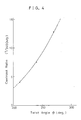
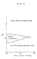
- the twist angle ⁇ is increased, the contrast ratio increases (see FIG. 4), hence desirable, whereas the range of d/p values settable without entailing improper orientation (undertwist domain or stripe domain) then tends to become smaller (see FIG. 5).
- the steepness of electrooptical characteristics of liquid crystal display devices differs with the cell construction and the liquid crystal composition used. If the steepness is insufficient, the contrast ratio (ratio of transmittance during ON-time to transmittance during OFF-time) is low to render the display difficult to view, whereas excessively steep characteristics give rise to a problem as to the nonuniformity of the display (especially halftone display) due to variations in the cell thickness in the display device. For this reason, the steepness of electrooptical characteristics of a particular liquid crystal display device must be set to a suitable range inherent in the cell structure of that device. For example, in the case of the liquid crystal display device having the cell structure shown in FIGS. 1 and 2 and usually exhibiting the electrooptical characteristics of FIG. 3, it has been found desirable to set the steepness of the characteristics to the range of 1.04 ⁇ V 90% /V 10% ⁇ 1.08.
- the present invention which has been accomplished to overcome the foregoing problems, provides a supertwisted nematic liquid crystal display device having a high response speed and adapted to give distinct display without entailing a reduced yield (increased cost).
- the compounds of the formulae (I) to (VII) for use in the present invention are known as components of liquid crystal compostions. However, no specific liquid crystal composition is known which is prepared from the combination of such components.
- the present invention provides a supertwisted nematic liquid crystal display device which comprises a pair of glass substrates each having an electrode and an orientation film formed on the surface of the electrode, and a liquid crystal composition comprising a base liquid crystal and optically active substance added thereto and interposed between the glass substrates so that the liquid crystal molecules have a twist angle ⁇ of 210 to 270°, the base liquid crystal comprising 10 wt. % to 30 wt. % of at least one compound represented by the formula (I): wherein R1 is a straight-chain or branched-chain alkyl group having up to 10 carbon atoms, 0 to 15 wt.
- R2 is a straight-chain or branched-chain alkyl group having up to 10 carbon atoms, 5 wt. % to 20 wt. % of at least one compound represented by the formula (III): wherein R3 is a straight-chain or branched-chain alkyl group having up to 10 carbon atoms, 15 wt. % to 35 wt. % of at least one compound represented by the formula (IV): wherein R4 and R5 are the same or different and are each a straight-chain or branched chain alkyl group having up to 10 carbon atoms, 10 wt. % to 25 wt.
- R6 and R7 are the same or different and are each a straight-chain or branched-chain alkyl group having up to 10 carbon atoms, 10 wt. % to 20 wt. % of at least one compound represented by the formula (VI): wherein R8 is a straight-chain or branched-chain alkyl group having up to 10 carbon atoms, and 0 to 10 wt. % of at least one compound represented by the formula (VII): wherein R9 is a straight-chain or branched-chain alkyl group having up to 10 carbon atoms.
- the supertwisted nematic liquid crystal display device of the present invention has a sufficient contrast ratio, a broad d/p margin exhibiting proper orientation and excellent response characteristics.
- a supertwisted nematic liquid crystal device which is free of the foregoing problems and which has a high response speed and a great contrast ratio can be fabricated by using a liquid crystal composition comprising as its base liquid crystal a liquid crystal mixture of specified quantities of compounds of the formulae (I), (III), (IV), (V) and (VI) in combination, and that (2) the device can be given improved low-temperature preservation stability (to remain free of crystallization at low temperatures) which is required especially for transport by air, by further adding compounds of the formulae (II) and (VII) to the liquid crystal mixture.
- the present invention is based on these findings.
- the liquid crystal composition for use in the present invention is prepared by adding small amounts of optically active compound to a base crystal which comprises compounds of the formulae (I), (III), (IV), (V) and (VI) and optional components, i.e., compounds of the formulae (II) and (VII).
- alkyl groups defined for the above formulae are methyl, ethyl, n-propyl, i-propyl, n-butyl, i-butyl, tert-butyl, pentyl, heptyl, hexyl, octyl, decyl, etc., among which C1 to C5 lower alkyl groups are desirable.
- the amount of compound of the formula (I) to present in the base crystal is 10 to 30 wt. %, preferably 20 to 30 wt. %.
- the compound of the formula (III) is used in an amount of 5 to 20 wt. %, preferably 10 to 20 wt. %; the compound of the formula (IV) in an amount of 15 to 35 wt. %, preferably 20 to 30 wt. %; the compound of the formula (V) in an amount of 10 to 25 wt. %, preferably 10 to 20 wt. %; and the compound of the formula (VI) in an amount of 10 to 20 wt. %, preferably 10 to 25 wt. %.
- the compound of the formula (II) is used in an amount of up to 15 wt. %, preferably 0 to 10 wt. %, and the compound of the formula (VII) in an amount of up to 10 wt. %, preferably 0 to 7 wt. %.
- Optically active compounds which are added to the base liquid crytal can be those already known in the art. These compounds are used in an amount sufficient to give a specified twist angle ⁇ (210 to 270°, preferably 235 to 245°).
- optically active compounds are, for example, those represented by the following formulae. wherein 2MB* denotes and C* denotes asymmetric carbon atom. Generally these compounds are used in an amount of 0.5 to 3.0 wt. % based on the base liquid crystal.
- the electrodes, orientation films, glass substrates, etc. for constituting the device of the invention can be those already known in the art.
- liquid crystal compounds from the groups represented by the following formulae A to N were used in combinations, with the proportion of each compound varied from 0 to 40 wt. % with increments or decrements of 5 wt. %, for preparing liquid crystal display devices which had the construction shown in FIG. 1 and wherein the twist angle ⁇ of liquid crystal molecules was 240° as shown in FIG. 2a.
- the devices were checked for contrast ratio (steepness of characteristics), response speed, d/p margin affording normal orientation, crystallization temperature in low temperature range, etc.
- R1 to R20 are the same or different and are each a straight-chain or branched-chain alkyl group having up to 10 carbon atoms.
- Compounds of the formula (VIII) were used as optically active compounds.
- Table 1 Item Requirement Steepness of characteristics V 10% /V 90% 1.055 to 1.065 d/p margin giving normal orientation At least 0.15 Low temperature crystallinity Not to crystallize at -25 degree C
- Compound group A 25 wt. %
- Compound group B 5 wt. %
- Compound group C 15 wt. %
- Compound group G 25 wt. %
- Compound group K 10 wt. % Compound group N 15 wt. %
- liquid crystal composition comprising specified proportions of specified compounds for use in the device of the present invention gives a high response speed and a great contrast ratio.
- a liquid crystal cell was prepared by forming patterns of transparent electrodes 3, 4 on the lower surface of an upper glass substrate 1 and on the upper surface of a lower glass substrate 2, respectively, from indium oxide, forming high-polymer orientation films 5, 6 of the polyimidosilane type over the respective electrodes 3, 4, and rubbing the surfaces of the films with a cloth in a given direction.
- Indicated at 8 is an upper polarizer, at 9 a lower polarizer, and at 7 a liquid crystal layer which was formed by injecting the liquid crystal composition to be described later into the cell.
- the orientation films 5, 6 were formed by applying a 30 wt.
- the solution is prepared by subjecting to condensation 0.1 mole of 1,3-bis(aminopropyl)-tetra methyldisiloxane, 0.9 mole of 4,4′-diaminodiphenyl ether and 1.0 mole of 3,3′,4,4′-benzophenonetetracarboxylic anhydride in N-methylpyrrolidone.
- FIGS. 2a and 2b are diagrams showing the relationship between the rubbing angle and the twist angle of liquid crystal molecules established for the liquid crystal display device of the above construction.
- the twist angle ⁇ of liquid crystal molecules is the same as the angle made by the rubbing direction 10 of the upper orientation film 5 and the rubbing direction 11 of the lower orientation film 6.
- the twist angle ⁇ is dependent on the ratio d/p wherein d is the thickness of the liquid crystal layer, and p is an inherent helical pitch induced by the addition of an optically active substance to a nematic liquid crystal.
- the ratio is adjusted to the range of: ( ⁇ /360° - 1/4) ⁇ d/p ⁇ ( ⁇ /360° + 1/4)
- liquid crystal compositions for use in the liquid crystal cell and the characteristics obtained when the compositions were used for liquid crystal display devices will be described below.
- a liquid crystal mixture was prepared from the components listed in Table 2, and was used for fabricating by the above method a supertwisted nematic liquid crystal device wherein the twist angle ⁇ of liquid crystal molecules was 240° and the cell thickness was 7.5 ⁇ m.
- the optically active compound added to the mixture was a compound of the formula (VIII) the same as in the exmaples to follow, and this compound was used in an amount of 1.40 wt. %.
- the device obtained had an exceedingly higher response speed and also a higher contrast ratio and was more exceelent in the reliability of orientation than the devices of comparative examples to be described later as will be apparent from Table 3.
- Table 3 (Measured at 25° C) Liquid crystal Twist angle ⁇ V 10% /V 90% 1) Response time ( ⁇ r, ⁇ d) 2) d/p margin Cell thickness ( ⁇ m) Ex. 1 240° 1.06 280 msec, 170 msec 0.17 7.5 Comp. Ex. 1 240° 1.06 320 msec, 210 msec 0.14 7.5 Comp. Ex. 2 240° 1.06 340 msec, 210 msec 0.14 7.5 Ex.
- a liquid crystal mixture was prepared from the components listed in Table 4, and was used for fabricating by the above method a supertwisted nematic liquid crystal device wherein the twist angle ⁇ of liquid crystal molecules was 210° and the cell thickness was 7.5 ⁇ m.
- the optically active compound was used in an amount of 1.20 wt. %.
- the device fabricated had a higher response speed than those of the comparative examples to be described below and was excellent in contrast ratio and in the reliabilty of orientation.
- a supertwisted nematic liquid crystal display device was prepared in the same manner as in Example 1 except that the components listed in Table 5 were used for preparing a liquid crystal mixture instead of the components given in Table 2.
- the device was low in response speed as shown in Table 3.
- a supertwisted nematic liquid crystal display device was fabricated in the same manner as in Example 1 except that the components listed in Table 6 were used for preparing a liquid crystal mixture in place of the components given in Table 2.
- the device was low in response speed as shown in Table 3.
- a supertwisted nematic liquid crystal display device was fabricated in the same manner as in Example 2 except that the components listed in Table 7 were used for preparing a liquid crystal mixture in place of the components given in Table 4.
- the device was low in response speed as shown in Table 3.
- a supertwisted nematic liquid crystal display device was fabricated in the same manner as in Example 2 except that the components listed in Table 8 were used for preparing a liquid crystal mixture in place of the components given in Table 4.
- the device was low in response speed as shown in Table 3.
- FIG. 6 is a diagram showing the relationship between V 90% /V 10% and the response time (sum of ⁇ r and ⁇ d) determined for the liquid crystal display devices which had incorporated therein the liquid crystal mixtures of the examples of the invention and the comparative examples and in which the twist angle ⁇ of liquid crystal molecules was 240°.
- FIG. 7 is a diagram showing like relationship established for liquid crystal display devices which had incorporated therein the liquid crystal mixtures of the examples and the comparative examples and in which the twist angle ⁇ was 210° (see FIG. 2b for the rubbing angle and polarizer axis setting angles).
- the diagrams show that as the value V 90% /V 10% decreases to increase the steepness of rise of the electrooptical characteristics of the display device, a longer response time tends to result.
- the mixture of the example is shorter in response time and more excellent in characteristics than the mixture of the comparative example.
- the former is also broader in d/p margin (see Table 3) exhibiting normal orientation and is superior in reliability.
- supertwisted nematic liquid crystal display devices can be provided which are given a satisfactory contrast ratio and a required d/p range with normal orientation without entailing an impaired production yield and which are remarkably improvied in response characteristics.
- the liquid crystal display devices which were fabricated with use of the liquid crystal mixture of the invention and in which the twist angle ⁇ of liquid crystal molecules was 240° and the thickness of the liquid crystal layer was 7.5 ⁇ m exhibited a sufficient contrast ratio, satisfactory response characteristics and reliable orientation free of problems when driven with duty of 1/240.
- liquid crystal mixture exhibits especially outstanding characteristics when providing liquid crystal devices wherein the twist angle ⁇ is in the range of 235° ⁇ ⁇ ⁇ 245°
- the mixture similarly exhibits a high contrast ratio and excellent response chracteristics when incorporated in devices wherein the angle ⁇ is in the range of 210° ⁇ ⁇ ⁇ 270°.
Landscapes
- Chemical & Material Sciences (AREA)
- Physics & Mathematics (AREA)
- Crystallography & Structural Chemistry (AREA)
- Engineering & Computer Science (AREA)
- Materials Engineering (AREA)
- Organic Chemistry (AREA)
- Nonlinear Science (AREA)
- Mathematical Physics (AREA)
- General Physics & Mathematics (AREA)
- Optics & Photonics (AREA)
- Liquid Crystal Substances (AREA)
- Liquid Crystal (AREA)
Applications Claiming Priority (2)
| Application Number | Priority Date | Filing Date | Title |
|---|---|---|---|
| JP1200050A JPH0363621A (ja) | 1989-07-31 | 1989-07-31 | スーパーツイステッド・ネマチック型液晶表示素子 |
| JP200050/89 | 1989-07-31 |
Publications (3)
| Publication Number | Publication Date |
|---|---|
| EP0411511A2 true EP0411511A2 (de) | 1991-02-06 |
| EP0411511A3 EP0411511A3 (en) | 1991-05-22 |
| EP0411511B1 EP0411511B1 (de) | 1993-10-06 |
Family
ID=16417996
Family Applications (1)
| Application Number | Title | Priority Date | Filing Date |
|---|---|---|---|
| EP90114510A Expired - Lifetime EP0411511B1 (de) | 1989-07-31 | 1990-07-27 | Superverdrillte nematische Flüssigkristallanzeigevorrichtung |
Country Status (5)
| Country | Link |
|---|---|
| US (1) | US5106529A (de) |
| EP (1) | EP0411511B1 (de) |
| JP (1) | JPH0363621A (de) |
| KR (1) | KR940001901B1 (de) |
| DE (1) | DE69003765T2 (de) |
Cited By (3)
| Publication number | Priority date | Publication date | Assignee | Title |
|---|---|---|---|---|
| EP0717093A3 (de) * | 1994-12-12 | 1996-06-26 | Chisso Corp | |
| EP0719849A1 (de) * | 1994-12-28 | 1996-07-03 | Chisso Corporation | Flüssigkristallzusammensetzung und Anzeigevorrichtung |
| EP1788064A1 (de) * | 2005-11-16 | 2007-05-23 | Chisso Corporation | Flüssigkristallzusammensetzung und Flüssigkristallanzeigevorrichtung |
Families Citing this family (5)
| Publication number | Priority date | Publication date | Assignee | Title |
|---|---|---|---|---|
| US5507975A (en) * | 1990-02-15 | 1996-04-16 | Sharp Kabushiki Kaisha | Ferroelectric liquid crystal display |
| TW255017B (de) * | 1991-12-26 | 1995-08-21 | Toshiba Co Ltd | |
| DE69318865T2 (de) * | 1992-03-03 | 1998-12-10 | Matsushita Electric Industrial Co., Ltd., Kadoma, Osaka | Verdrillt-nematische Flüssigkristall-Anzeigevorrichtung mit aktiver Matrix |
| US5302970A (en) * | 1992-06-22 | 1994-04-12 | Abovo, Inc. | Personal communication device |
| WO1996034071A1 (en) * | 1995-04-25 | 1996-10-31 | Chisso Corporation | Liquid crystal composition and liquid crystal display element |
Family Cites Families (7)
| Publication number | Priority date | Publication date | Assignee | Title |
|---|---|---|---|---|
| JPS5939876A (ja) * | 1982-08-26 | 1984-03-05 | Chisso Corp | ピリミジン誘導体 |
| DE3404116A1 (de) * | 1984-02-07 | 1985-08-08 | Merck Patent Gmbh, 6100 Darmstadt | Stickstoffhaltige heterocyclen |
| JPS62194224A (ja) * | 1986-02-20 | 1987-08-26 | Sharp Corp | ツイステツド・ネマチツク型液晶表示素子 |
| JPS63167331A (ja) * | 1986-12-29 | 1988-07-11 | Sharp Corp | ツイステツド・ネマチツク型液晶表示素子 |
| JP2594583B2 (ja) * | 1987-11-10 | 1997-03-26 | シャープ株式会社 | 液晶表示装置 |
| JP2660702B2 (ja) * | 1987-12-14 | 1997-10-08 | チッソ株式会社 | 液晶組成物 |
| US4946986A (en) * | 1988-02-29 | 1990-08-07 | Dainippon Ink And Chemicals | Cyclohexene derivatives |
-
1989
- 1989-07-31 JP JP1200050A patent/JPH0363621A/ja active Pending
-
1990
- 1990-07-27 EP EP90114510A patent/EP0411511B1/de not_active Expired - Lifetime
- 1990-07-27 DE DE90114510T patent/DE69003765T2/de not_active Expired - Fee Related
- 1990-07-30 US US07/559,308 patent/US5106529A/en not_active Expired - Lifetime
- 1990-07-30 KR KR1019900011598A patent/KR940001901B1/ko not_active Expired - Lifetime
Cited By (4)
| Publication number | Priority date | Publication date | Assignee | Title |
|---|---|---|---|---|
| EP0717093A3 (de) * | 1994-12-12 | 1996-06-26 | Chisso Corp | |
| EP0719849A1 (de) * | 1994-12-28 | 1996-07-03 | Chisso Corporation | Flüssigkristallzusammensetzung und Anzeigevorrichtung |
| EP1788064A1 (de) * | 2005-11-16 | 2007-05-23 | Chisso Corporation | Flüssigkristallzusammensetzung und Flüssigkristallanzeigevorrichtung |
| US7563492B2 (en) | 2005-11-16 | 2009-07-21 | Chisso Corporation | Liquid crystal composition and liquid crystal display device |
Also Published As
| Publication number | Publication date |
|---|---|
| EP0411511A3 (en) | 1991-05-22 |
| KR940001901B1 (ko) | 1994-03-11 |
| EP0411511B1 (de) | 1993-10-06 |
| KR910003423A (ko) | 1991-02-27 |
| DE69003765T2 (de) | 1994-04-28 |
| US5106529A (en) | 1992-04-21 |
| JPH0363621A (ja) | 1991-03-19 |
| DE69003765D1 (de) | 1993-11-11 |
Similar Documents
| Publication | Publication Date | Title |
|---|---|---|
| JP2700006B2 (ja) | 液晶表示素子 | |
| US4856875A (en) | Liquid-crystal display devices of twisted nematic type | |
| DE69521458T2 (de) | Flüssigkristallzusammensetzung, -vorrichtung, -apparat und Anzeigeverfahren, die sie verwenden | |
| KR930005336B1 (ko) | 액정 표시소자 | |
| DE69204855T2 (de) | Ferroelektrische Flüssigkristallzusammensetzung sowie Flüssigkristallvorrichtung zu deren Verwendung. | |
| EP0411511A2 (de) | Superverdrillte nematische Flüssigkristallanzeigevorrichtung | |
| DE69313179T2 (de) | Flüssigkristallvorrichtung und -apparat | |
| KR970008263B1 (ko) | 액정 조성물 | |
| US4913530A (en) | Liquid crystal display | |
| US5089169A (en) | Liquid crystal material and display device using same | |
| EP0312983B1 (de) | Flüssigkristallzusammensetzung und dieselbe verwendende Flüssigkristallanzeigevorrichtung | |
| KR100188314B1 (ko) | 저전압구동용 액정 재료 및 이 액정재료를 사용한 액정표시판 | |
| EP0176039A2 (de) | Flüssigkristallzusammensetzung | |
| JPH052718B2 (de) | ||
| JP2901157B2 (ja) | 液晶組成物 | |
| JP2958046B2 (ja) | 強誘電性液晶組成物 | |
| JPS647116B2 (de) | ||
| JPS6334918B2 (de) | ||
| JPH0540281A (ja) | Tn型液晶表示素子 | |
| JPS643239B2 (de) | ||
| JP3625862B2 (ja) | 液晶材料及び液晶表示パネル | |
| JP3637932B2 (ja) | 液晶組成物および液晶表示素子 | |
| JP2629894B2 (ja) | 液晶組成物およびそれを用いた液晶表示素子 | |
| JP3128880B2 (ja) | 液晶組成物およびそれを用いた液晶表示素子 | |
| JPS63186217A (ja) | 液晶表示装置 |
Legal Events
| Date | Code | Title | Description |
|---|---|---|---|
| PUAI | Public reference made under article 153(3) epc to a published international application that has entered the european phase |
Free format text: ORIGINAL CODE: 0009012 |
|
| 17P | Request for examination filed |
Effective date: 19900727 |
|
| AK | Designated contracting states |
Kind code of ref document: A2 Designated state(s): DE FR GB NL |
|
| PUAL | Search report despatched |
Free format text: ORIGINAL CODE: 0009013 |
|
| AK | Designated contracting states |
Kind code of ref document: A3 Designated state(s): DE FR GB NL |
|
| 17Q | First examination report despatched |
Effective date: 19921014 |
|
| GRAA | (expected) grant |
Free format text: ORIGINAL CODE: 0009210 |
|
| AK | Designated contracting states |
Kind code of ref document: B1 Designated state(s): DE FR GB NL |
|
| REF | Corresponds to: |
Ref document number: 69003765 Country of ref document: DE Date of ref document: 19931111 |
|
| ET | Fr: translation filed | ||
| PLBE | No opposition filed within time limit |
Free format text: ORIGINAL CODE: 0009261 |
|
| STAA | Information on the status of an ep patent application or granted ep patent |
Free format text: STATUS: NO OPPOSITION FILED WITHIN TIME LIMIT |
|
| 26N | No opposition filed | ||
| PGFP | Annual fee paid to national office [announced via postgrant information from national office to epo] |
Ref country code: FR Payment date: 20010712 Year of fee payment: 12 |
|
| PGFP | Annual fee paid to national office [announced via postgrant information from national office to epo] |
Ref country code: DE Payment date: 20010723 Year of fee payment: 12 |
|
| PGFP | Annual fee paid to national office [announced via postgrant information from national office to epo] |
Ref country code: GB Payment date: 20010725 Year of fee payment: 12 |
|
| PGFP | Annual fee paid to national office [announced via postgrant information from national office to epo] |
Ref country code: NL Payment date: 20010730 Year of fee payment: 12 |
|
| REG | Reference to a national code |
Ref country code: GB Ref legal event code: IF02 |
|
| PG25 | Lapsed in a contracting state [announced via postgrant information from national office to epo] |
Ref country code: GB Free format text: LAPSE BECAUSE OF NON-PAYMENT OF DUE FEES Effective date: 20020727 |
|
| PG25 | Lapsed in a contracting state [announced via postgrant information from national office to epo] |
Ref country code: NL Free format text: LAPSE BECAUSE OF NON-PAYMENT OF DUE FEES Effective date: 20030201 Ref country code: DE Free format text: LAPSE BECAUSE OF NON-PAYMENT OF DUE FEES Effective date: 20030201 |
|
| GBPC | Gb: european patent ceased through non-payment of renewal fee |
Effective date: 20020727 |
|
| PG25 | Lapsed in a contracting state [announced via postgrant information from national office to epo] |
Ref country code: FR Free format text: LAPSE BECAUSE OF NON-PAYMENT OF DUE FEES Effective date: 20030331 |
|
| NLV4 | Nl: lapsed or anulled due to non-payment of the annual fee |
Effective date: 20030201 |
|
| REG | Reference to a national code |
Ref country code: FR Ref legal event code: ST |