EP0411530A2 - Structuration d'un conducteur transparent - Google Patents
Structuration d'un conducteur transparent Download PDFInfo
- Publication number
- EP0411530A2 EP0411530A2 EP90114580A EP90114580A EP0411530A2 EP 0411530 A2 EP0411530 A2 EP 0411530A2 EP 90114580 A EP90114580 A EP 90114580A EP 90114580 A EP90114580 A EP 90114580A EP 0411530 A2 EP0411530 A2 EP 0411530A2
- Authority
- EP
- European Patent Office
- Prior art keywords
- film
- transparent conducting
- conducting film
- etching
- silicon
- Prior art date
- Legal status (The legal status is an assumption and is not a legal conclusion. Google has not performed a legal analysis and makes no representation as to the accuracy of the status listed.)
- Granted
Links
Images





Classifications
-
- H—ELECTRICITY
- H10—SEMICONDUCTOR DEVICES; ELECTRIC SOLID-STATE DEVICES NOT OTHERWISE PROVIDED FOR
- H10F—INORGANIC SEMICONDUCTOR DEVICES SENSITIVE TO INFRARED RADIATION, LIGHT, ELECTROMAGNETIC RADIATION OF SHORTER WAVELENGTH OR CORPUSCULAR RADIATION
- H10F71/00—Manufacture or treatment of devices covered by this subclass
- H10F71/138—Manufacture of transparent electrodes, e.g. transparent conductive oxides [TCO] or indium tin oxide [ITO] electrodes
-
- Y—GENERAL TAGGING OF NEW TECHNOLOGICAL DEVELOPMENTS; GENERAL TAGGING OF CROSS-SECTIONAL TECHNOLOGIES SPANNING OVER SEVERAL SECTIONS OF THE IPC; TECHNICAL SUBJECTS COVERED BY FORMER USPC CROSS-REFERENCE ART COLLECTIONS [XRACs] AND DIGESTS
- Y02—TECHNOLOGIES OR APPLICATIONS FOR MITIGATION OR ADAPTATION AGAINST CLIMATE CHANGE
- Y02E—REDUCTION OF GREENHOUSE GAS [GHG] EMISSIONS, RELATED TO ENERGY GENERATION, TRANSMISSION OR DISTRIBUTION
- Y02E10/00—Energy generation through renewable energy sources
- Y02E10/50—Photovoltaic [PV] energy
-
- Y—GENERAL TAGGING OF NEW TECHNOLOGICAL DEVELOPMENTS; GENERAL TAGGING OF CROSS-SECTIONAL TECHNOLOGIES SPANNING OVER SEVERAL SECTIONS OF THE IPC; TECHNICAL SUBJECTS COVERED BY FORMER USPC CROSS-REFERENCE ART COLLECTIONS [XRACs] AND DIGESTS
- Y10—TECHNICAL SUBJECTS COVERED BY FORMER USPC
- Y10S—TECHNICAL SUBJECTS COVERED BY FORMER USPC CROSS-REFERENCE ART COLLECTIONS [XRACs] AND DIGESTS
- Y10S438/00—Semiconductor device manufacturing: process
- Y10S438/963—Removing process residues from vertical substrate surfaces
Definitions
- the present invention relates to the patterning of transparent conducting film and particularly to a method of patterning transparent conducting film formed on a substrate including silicon.
- an amorphous silicon (a-Si) film suitable for receiving visible light an amorphous silicon carbide (a-SiC) film, or a multilayered film comprising such films is used.
- a transparent conducting film indium (In) . tin (Sn) . oxide film (ITO film), for example, is used. Fabrication of such films is very important in the fabrication of imaging devices.
- Figs. 1(a) to 1(e) are schematic sectional views for assistance in explaining parts of a conventional fabrication process for producing an imaging device.
- Fig. 1(a) shows a sample structure immediately before formation of a transparent conducting film, where a multilayered film consisting of a-SiC film/a-Si film/a-SiC film is formed as a light receiving part.
- the structures shown in Figs. 1(a) to (e) are referred to as the "sample” in the following description of fabrication process steps).
- a collector electrode for charges generated through photoelectric conversion, a charge storage diode and a CCD (charge coupled device) for transferring charges have a well-known structure and are not illustrated.
- Fig. 1(b) the sample of Fig. 1(a) is placed into a sputtering apparatus, substrate temperature is raised (up to about 150°C) and thereafter a first transparent conducting film 8 consisting of ITO is formed by sputtering on the a-SiC film 7d.
- the substrate is heated to improve adhesive strength between the substrate and transparent conducting film and also to improve light receiving characteristics.
- a resist pattern 9 is formed on the first transparent conducting film 8 and this first transparent conducting film 8 is then removed by etching using an aqueous solution of ferric chloride (FeCl3) with the resist pattern 9 used as a mask.
- FeCl3 ferric chloride
- Such wet etching is carried out here because, since the vapour pressure of indium (In) and tin (Sn) is low, etching rate is low for dry etching of ITO.
- a-SiC film 7d/a-Si film 7c/a-SiC film 7b is etched by nitrogen trifluoride (NF3)
- NF3 nitrogen trifluoride
- the PSG film 6 on the Al wiring 5 is selectively etched and thereby an aperture 10 is formed.
- this sample is put into sputtering apparatus and a second transparent conducting film 11 is formed on the sample surface under the same conditions as for formation of the first transparent conducting film 8.
- the Al wiring 5 is connected to the second transparent conducting film 11 through the aperture 10.
- a resist pattern 12 is formed on the second transparent conducting film 11 and the second transparent conducting film 11 is etched by a FeCl3 aqueous solution with the resist pattern used as mask. As explained above, a leadout electrode 11c is formed, completing an imaging device.
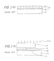
- an interfacial reacted layer 8a is generated by reaction of ITO and Si at the interface between the first transparent conducting film 8 and the a-SiC film 7d, as shown in Fig. 2(a).
- This interfacial reacted layer 8a does not easily dissolve into the aqueous solution of FeCl3. Therefore, when etching time is set longer in order to ensure complete removal of the interfacial reacted layer 8a shown in Fig. 2(a), lateral etching of the first transparent conducting film 8b, where ITO has not reacted with Si, proceeds as shown in Fig.
- the ITO film may easily peel off and light transmissivity become small, so that the structure can no longer be put to practical use.
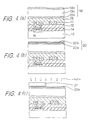
- the phenomenon occurring on the first transparent conducting film 8 also occurs in the formation of the second transparent conducting film 11 made of ITO film. Namely, as shown in Fig. 3(a), a side product layer 11a is generated by reaction of ITO and Si included in the PSG film 6 at the interface between the second transparent conducting film 11 and PSG film 6. Therefore, if an attempt is made to completely remove the interfacial reacted layer 11a when the second transparent conducting film 11 is etched, as shown in Fig. 1(e), the ITO film 11b is etched laterally as shown in Fig. 3(b), and the etchant sometimes reaches the Al wiring 5. In this case, the Al wiring 5 may be etched because the etchant includes chlorine. As a result, a problem of deterioration of imaging device quality occurs.
- An embodiment of the present invention can provide a method of etching a transparent conducting film, on a substrate including Si, which offers adequate etching rate.
- An embodiment of the present invention can provide a method of etching a transparent conducting film, on a substrate including Si, which does not lead to deterioration of device characteristics.
- An embodiment of the present invention can provide a method of patterning a transparent conducting film, on a substrate including Si, offering high accuracy.
- An embodiment of the present invention may be effected by carrying out etching comprising steps for forming a transparent conducting film such as ITO on a substrate including Si element and executing wet etching of the transparent conducting film with a halogenide etchant and then dry etching with a reactive gas including a halogen element with a resist pattern formed on the transparent conducting film used as a mask.
- etching comprising steps for forming a transparent conducting film such as ITO on a substrate including Si element and executing wet etching of the transparent conducting film with a halogenide etchant and then dry etching with a reactive gas including a halogen element with a resist pattern formed on the transparent conducting film used as a mask.
- a transparent conducting film for example indium . tin oxide film (ITO film), aluminium . zinc oxide film (AZO) film, indium oxide film (In2O3 film), tin oxide film (SnO2 film) or zinc oxide film (ZnO film), is grown at a temperature of 100°C or higher, an interfacial reacted layer produced by reaction of ITO, AZO, In2O3, SnO2 or ZnO with Si is formed at the interface between the substrate and transparent conducting film.
- ITO film indium . tin oxide film
- AZO aluminium . zinc oxide film
- In2O3 film indium oxide film
- SnO2 film tin oxide film
- ZnO film zinc oxide film
- ITO, AZO, In2O3, SnO2, ZnO films are etched at an adequate etching rate by an halogenide etchant but the interfacial reacted layer produced by reaction does not easily dissolve into the halogenide etchant.
- the inventors have had the insight that since the interfacial reacted layer includes Si, it can be etched at an adequate etching rate by dry etching using reactive gas including a halogen element even though ITO, AZO, In2O3, SnO2, ZnO films have a property of not being dry-etched by a gas as described above.
- the inventors when etching a transparent conducting film formed on a substrate including Si element, the inventors have had the insight that an adequate etching rate may be maintained by carrying out an etching process consisting of two steps such that the upper layer part of a transparent conducting film (the region where an interfacial reacted layer is not formed by reaction with Si) is wet-etched by an halogenide etchant and thereafter the interfacial reacted layer is dry-etched with a reactive gas including an halogen element.
- side etching of the transparent conducting film of the upper layer may be significantly reduced.
- patterning of a transparent conducting film can be effected with highly accurate matching to the size of pattern of an etching resistant film, for example a resist pattern.
- increase of leakage current due to irregular etching in the periphery of a light receiving region can be prevented and deterioration of characteristics arising from etching of an electrode can also be prevented.
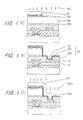
- Fig. 4(a) 13 is a Si substrate; 14 is a SiO2 film for device separation; 15 is an interlayer insulation film; 16 is a transistor for amplification; 17 is Al wiring, 18 is a PSG film for flattening (planarization); 19 is a light receiving region consisting of a-SiC film/a-Si film/a-SiC film.
- a collector electrode for charges generated through photoelectric conversion, a diode for charge storage and a CCD for charge transfer are not illustrated.
- a sample as shown in the Figure is placed into sputtering apparatus and is kept at a temperature of about 150°C and, during this period, a first transparent conducting film consisting of ITO film is formed on a-SiC film 19d by the sputtering method.
- a first transparent conducting film consisting of ITO film is formed on a-SiC film 19d by the sputtering method.
- an interfacial reacted layer 20a of Si and ITO is formed at the interface between the a-SiC film 19d and the first transparent conducting film 20, and a part 20b of the ITO where an interfacial reacted layer does not exist is left as an upper layer.
- a resist pattern 21 is formed on the ITO film 20b and the ITO film 20b is etched, first at 30°C to 60°C by an aqueous solution of ferric chloride (FeCl3) with the resist pattern 21 used as the mask.
- a preferable temperature is 40°C.
- the concentration of the aqueous solution should be in the range 30% to 40%, and a preferable concentration is 35%. In this case, etching rate is 200 to 1000 ⁇ /min.
- hydrochloric acid HCl
- HNO3 hydrochloric acid
- HI hydroiodic acid
- HBr hydrobromic acid
- the interfacial reacted layer 20a is etched by a plasma etching method using nitrogen trifluoride (NF3) gas.
- NF3 nitrogen trifluoride
- Exemplary conditions for this plasma etching are as follows. NF3 at 150 SCCM is supplied to the plasma etching chamber and the pressure is kept at 0.3 to 1.0 Torr. (The preferable pressure is 0.6 Torr). The sample is kept at 60°C.
- the plasma generating frequency is 13.56 MHz and the power is in the range from 0.05 W/cm2 to 0.3 W/cm2. Under these conditions, etching rate for a-Si is set to 2000 ⁇ /min.
- the interfacial reacted layer 20a remains almost unetched after etching with 35% aqueous solution of the ferric chloride (FeCl3) and therefore here the etching process is switched to plasma etching.
- the Si element included in the interfacial reacted layer 20a is etched because it reacts with NF3 to generate silicon tetrafluoride (SiF4). Therefore, this plasma etching provides an adequate etching rate. Accordingly, the extent of side etching of ITO film 20b can be reduced remarkably as shown in Fig. 5(b).
- the first transparent conducting film 20 can be patterned with a high accuracy in accordance with the resist pattern 21. Moreover, since the light receiving part 19 under the resist pattern 21 is always covered with the ITO film 20b, deterioration of the heterojunction at the light receiving part can be prevented.
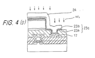
- the a-SiC film 19d/a-Si film 19c/a-SiC film 19b are etched under similar conditions, and the PSG film 18 on the Al wiring 17 is selectively etched to form the aperture 22.
- the sample is then put into the sputtering apparatus, kept at 150°C, and second transparent conducting film 23 consisting of ITO film is formed by the sputtering method. Thereby, the Al wiring 17 and the second transparent conducting film 23 are connected through the aperture 22.
- an interfacial reacted layer 23a produced by reaction of Si element included in the PSG film 18 and ITO is formed at the interface of the PSG film 18 and the second transparent conducting film 23.
- An ITO film 23b, other than the interfacial reacted layer 23a, remains as an upper layer of second transparent conducting film 23 which has not generated an interfacial reacted layer by reaction.
- the ITO film 23b is etched by aqueous solution of ferric chloride (FeCl3) with resist pattern 24 used as the mask.
- aqueous solution of ferric chloride (FeCl3) ferric chloride (FeCl3) with resist pattern 24 used as the mask.
- interfacial reacted layer 23a is not easily etched by the aqueous solution and remains in place.
- the interfacial reacted layer 23a is etched by the plasma etching method using NF3, to form a leadout electrode 23c.
- the interfacial reacted layer 23a includes Si element, and NF3 has an adequate etching rate for the interfacial reacted layer 23a.
- the interfacial reacted layer 23a and ITO film 23b are patterned with high accuracy depending on the resist pattern 24 and the Al wiring 17 as the lower layer is not etched, unlike the situation shown in Fig. 3(b).
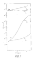
- Fig. 7 shows respective current voltage characteristics of photo current (I Ph ) and dark current (I d ) of an a-Si photo diode fabricated using an embodiment of the present invention.
- current - voltage characteristics of photo current (I Ph ) and dark current (I d ) of an a-Si photo diode fabricated using the conventional etching method are shown for the purpose of comparison.
- curves (1) relate to current -voltage characteristics of the a-Si photo diode fabricated using an etching method in accordance with an embodiment of the present invention
- curves (2) relate to the current - voltage characteristics of a similar a-Si photo diode fabricated using the conventional etching method.
- I d and I Ph of the a-Si photo diode fabricated using the etching method of an embodiment of the present invention show little change in the voltage range from 0 to 10 volts. This means that the etching method of the present invention does not in essence cause any increase of leakage current.
- NF3 was used as the gas for plasma etching the interfacial reacted layer of ITO and Si, but the following gases can also be used, providing an effect similar to NF3.
- the other conditions may be the same as those for NF3 or may be somewhat changed, as required.
- the gases are:- fluorine (F2), nitrogen trifluoride (NF3), tetrafluoromethane (CF4), hexafluoroethane(C 2F 6) , octafluoropropane (C3F8), hydrogen fluoride (HF), chlorine (Cl2), tetrachloromethane (CCl4), hydrogen chloride (HCl), dichlorosilane (SiH2Cl2), tetrachloro-difluoroethane (C2F2Cl4), trifluoromethane (CHF3), bromine (Br2), hydrogen bromide (HBr).
- Si substrate In the described embodiment a silicon (Si) substrate was referred to.
- substrate materials for example:- silicon, silicon carbide (SiC), silicon-germanium(SiGe),spin-on-glass (SOG), phosphosilicate glass (PSG), silicon dioxide (SiO2), borophosphosilicate glass (BPSG).
- ITO film which may be used in embodiments of the present invention are, for example, indium oxide and zinc oxide film. Mixtures of such materials may be used.
- etchant alternatives to an aqueous solution of ferric chloride, as etchant, which may be used in embodiments of the present invention are hydrochloric acid, hydroiodic acid, hydrobromic acid, and a mixed acid of hydrochloric acid and nitric acid for example.
- An embodiment of the present invention provides a method of forming a pattern of a transparent conducting film such as ITO film formed on the surface of a substrate including Si element, being heated, by employing a two-step etching method, in which such transparent conducting film is wet-etched by an aqueous solution of halogenide and thereafter an interfacial reacted layer generated at the interface of the transparent conducting film and substrate including Si element is etched by a plasma etching method using halogen element.
Landscapes
- Drying Of Semiconductors (AREA)
- Light Receiving Elements (AREA)
- Weting (AREA)
- Solid State Image Pick-Up Elements (AREA)
Applications Claiming Priority (2)
| Application Number | Priority Date | Filing Date | Title |
|---|---|---|---|
| JP1198747A JPH0362968A (ja) | 1989-07-31 | 1989-07-31 | 半導体装置の製造方法 |
| JP198747/89 | 1989-07-31 |
Publications (3)
| Publication Number | Publication Date |
|---|---|
| EP0411530A2 true EP0411530A2 (fr) | 1991-02-06 |
| EP0411530A3 EP0411530A3 (en) | 1991-04-03 |
| EP0411530B1 EP0411530B1 (fr) | 1995-02-08 |
Family
ID=16396295
Family Applications (1)
| Application Number | Title | Priority Date | Filing Date |
|---|---|---|---|
| EP90114580A Expired - Lifetime EP0411530B1 (fr) | 1989-07-31 | 1990-07-30 | Structuration d'un conducteur transparent |
Country Status (3)
| Country | Link |
|---|---|
| US (1) | US5094978A (fr) |
| EP (1) | EP0411530B1 (fr) |
| JP (1) | JPH0362968A (fr) |
Cited By (3)
| Publication number | Priority date | Publication date | Assignee | Title |
|---|---|---|---|---|
| EP0608931A3 (fr) * | 1993-01-25 | 1994-11-23 | Philips Electronics Nv | Gravure ionique réactive d'oxyde d'étain et d'indium. |
| EP0978883A4 (fr) * | 1998-01-28 | 2002-01-30 | Citizen Watch Co Ltd | Procede de fabrication d'un dispositif de pile solaire |
| US10453986B2 (en) | 2008-01-23 | 2019-10-22 | Solvay Fluor Gmbh | Process for the manufacture of solar cells |
Families Citing this family (18)
| Publication number | Priority date | Publication date | Assignee | Title |
|---|---|---|---|---|
| JP2814155B2 (ja) * | 1990-08-13 | 1998-10-22 | キヤノン株式会社 | Ito膜パターンの形成方法および液晶表示素子用基板の製造方法 |
| KR950000900B1 (ko) * | 1991-03-18 | 1995-02-03 | 주식회사 에스 · 케이 · 씨 | 광기록매체의 제조방법 |
| US5466618A (en) * | 1993-12-29 | 1995-11-14 | Goldstar Co., Ltd. | Method for fabricating a thin film transistor for a liquid crystal display |
| US5607602A (en) * | 1995-06-07 | 1997-03-04 | Applied Komatsu Technology, Inc. | High-rate dry-etch of indium and tin oxides by hydrogen and halogen radicals such as derived from HCl gas |
| US5843277A (en) * | 1995-12-22 | 1998-12-01 | Applied Komatsu Technology, Inc. | Dry-etch of indium and tin oxides with C2H5I gas |
| US6373117B1 (en) * | 1999-05-03 | 2002-04-16 | Agilent Technologies, Inc. | Stacked multiple photosensor structure including independent electrical connections to each photosensor |
| JP4677654B2 (ja) * | 2000-04-19 | 2011-04-27 | 日本電気株式会社 | 透過型液晶表示装置及びその製造方法 |
| US7547635B2 (en) * | 2002-06-14 | 2009-06-16 | Lam Research Corporation | Process for etching dielectric films with improved resist and/or etch profile characteristics |
| EP1998373A3 (fr) * | 2005-09-29 | 2012-10-31 | Semiconductor Energy Laboratory Co, Ltd. | Dispositif de semi-conducteur disposant d'une couche de semi-conducteur d'oxyde et son procédé de fabrication |
| KR101303578B1 (ko) * | 2007-01-05 | 2013-09-09 | 삼성전자주식회사 | 박막 식각 방법 |
| JP2010074072A (ja) * | 2008-09-22 | 2010-04-02 | Nec Corp | 半導体装置および半導体装置の製造方法 |
| SG187274A1 (en) * | 2011-07-14 | 2013-02-28 | 3M Innovative Properties Co | Etching method and devices produced using the etching method |
| WO2013019695A2 (fr) | 2011-08-04 | 2013-02-07 | 3M Innovative Properties Company | Ensembles barrières à bord protégé |
| JP5946132B2 (ja) * | 2012-09-25 | 2016-07-05 | 富士フイルム株式会社 | 固体撮像素子の製造方法 |
| US9099222B2 (en) | 2012-10-10 | 2015-08-04 | Carestream Health, Inc. | Patterned films and methods |
| US9904386B2 (en) * | 2014-01-23 | 2018-02-27 | 3M Innovative Properties Company | Method for patterning a microstructure |
| CN103972075A (zh) * | 2014-05-05 | 2014-08-06 | 京东方科技集团股份有限公司 | 一种刻蚀方法和阵列基板 |
| JP6692306B2 (ja) * | 2017-02-09 | 2020-05-13 | 株式会社東芝 | 半導体装置、半導体装置の製造方法、インバータ回路、駆動装置、車両、及び、昇降機 |
Family Cites Families (9)
| Publication number | Priority date | Publication date | Assignee | Title |
|---|---|---|---|---|
| US3979240A (en) * | 1975-05-02 | 1976-09-07 | General Electric Company | Method of etching indium tin oxide |
| NL7509341A (nl) * | 1975-08-06 | 1977-02-08 | Philips Nv | Werkwijze voor de vervaardiging van elektrisch geleidende indiumoxide patronen op een isole- rende drager. |
| DE2929589A1 (de) * | 1979-07-04 | 1981-01-22 | Bbc Brown Boveri & Cie | Verfahren zur herstellung eines optisch transparenten und elektrisch leitfaehigen filmmusters |
| US4336295A (en) * | 1980-12-22 | 1982-06-22 | Eastman Kodak Company | Method of fabricating a transparent metal oxide electrode structure on a solid-state electrooptical device |
| US4544444A (en) * | 1984-08-15 | 1985-10-01 | General Motors Corporation | Reactive ion etching of tin oxide films using silicon tetrachloride reactant gas |
| US4670097A (en) * | 1985-12-23 | 1987-06-02 | Gte Products Corporation | Method for patterning transparent layers on a transparent substrate |
| US4750980A (en) * | 1986-11-07 | 1988-06-14 | Texas Instruments Incorporated | Process for etching tin oxide |
| US4708766A (en) * | 1986-11-07 | 1987-11-24 | Texas Instruments Incorporated | Hydrogen iodide etch of tin oxide |
| US4878993A (en) * | 1988-12-22 | 1989-11-07 | North American Philips Corporation | Method of etching thin indium tin oxide films |
-
1989
- 1989-07-31 JP JP1198747A patent/JPH0362968A/ja active Pending
-
1990
- 1990-07-19 US US07/554,367 patent/US5094978A/en not_active Expired - Lifetime
- 1990-07-30 EP EP90114580A patent/EP0411530B1/fr not_active Expired - Lifetime
Cited By (3)
| Publication number | Priority date | Publication date | Assignee | Title |
|---|---|---|---|---|
| EP0608931A3 (fr) * | 1993-01-25 | 1994-11-23 | Philips Electronics Nv | Gravure ionique réactive d'oxyde d'étain et d'indium. |
| EP0978883A4 (fr) * | 1998-01-28 | 2002-01-30 | Citizen Watch Co Ltd | Procede de fabrication d'un dispositif de pile solaire |
| US10453986B2 (en) | 2008-01-23 | 2019-10-22 | Solvay Fluor Gmbh | Process for the manufacture of solar cells |
Also Published As
| Publication number | Publication date |
|---|---|
| EP0411530B1 (fr) | 1995-02-08 |
| EP0411530A3 (en) | 1991-04-03 |
| US5094978A (en) | 1992-03-10 |
| JPH0362968A (ja) | 1991-03-19 |
Similar Documents
| Publication | Publication Date | Title |
|---|---|---|
| EP0411530B1 (fr) | Structuration d'un conducteur transparent | |
| US4680085A (en) | Method of forming thin film semiconductor devices | |
| US5188970A (en) | Method for forming an infrared detector having a refractory metal | |
| EP0779654B1 (fr) | Procédé de fabrication d'ouvertures dans une couche de passivation d'un dispositif semi-conducteur | |
| US6627866B2 (en) | Optical barrier and methods for forming the optical barrier without etching a transparent layer below the optical barrier | |
| US5370972A (en) | Amorphous silicon photodiode with sloped sidewalls and method of fabrication | |
| EP0978883B1 (fr) | Procede de fabrication d'une cellule solaire | |
| KR100888200B1 (ko) | 반도체소자의 전도 패턴 형성 방법 | |
| US20190109253A1 (en) | Solar cell and method for manufacturing same, and solar cell panel | |
| JPH0766437A (ja) | 光電変換装置用基板の製造方法 | |
| KR100617076B1 (ko) | 듀얼 다마신 형성방법 | |
| KR100445060B1 (ko) | 반도체장치의금속배선형성방법 | |
| JPWO1999039390A1 (ja) | 太陽電池装置の製造方法 | |
| JPH0745587A (ja) | 半導体装置の製造方法 | |
| US5132761A (en) | Method and apparatus for forming an infrared detector having a refractory metal | |
| KR100490299B1 (ko) | 플래시 메모리 소자의 제조 방법 | |
| KR100298450B1 (ko) | 반도체소자의제조방법 | |
| WO1999021221A1 (fr) | Procedes de formation d'elements conducteurs et de lignes conductrices | |
| JP2806021B2 (ja) | 半導体装置の製造方法 | |
| JP3539748B2 (ja) | 半導体装置の製造方法 | |
| KR100673142B1 (ko) | 게이트 전극 형성 방법 | |
| JPH06181300A (ja) | 半導体装置及びその製造方法 | |
| KR19980026991A (ko) | 반도체장치의 접촉 홀 형성방법 | |
| JPH0246772A (ja) | 薄膜素子の製造方法 | |
| JPH06326129A (ja) | 薄膜トランジスタとその製造方法 |
Legal Events
| Date | Code | Title | Description |
|---|---|---|---|
| PUAI | Public reference made under article 153(3) epc to a published international application that has entered the european phase |
Free format text: ORIGINAL CODE: 0009012 |
|
| AK | Designated contracting states |
Kind code of ref document: A2 Designated state(s): DE FR GB |
|
| PUAL | Search report despatched |
Free format text: ORIGINAL CODE: 0009013 |
|
| AK | Designated contracting states |
Kind code of ref document: A3 Designated state(s): DE FR GB |
|
| RHK1 | Main classification (correction) |
Ipc: H01L 31/18 |
|
| 17P | Request for examination filed |
Effective date: 19910411 |
|
| 17Q | First examination report despatched |
Effective date: 19931103 |
|
| RBV | Designated contracting states (corrected) |
Designated state(s): FR |
|
| GRAA | (expected) grant |
Free format text: ORIGINAL CODE: 0009210 |
|
| REG | Reference to a national code |
Ref country code: DE Ref legal event code: 8566 |
|
| AK | Designated contracting states |
Kind code of ref document: B1 Designated state(s): FR |
|
| ET | Fr: translation filed | ||
| PLBE | No opposition filed within time limit |
Free format text: ORIGINAL CODE: 0009261 |
|
| STAA | Information on the status of an ep patent application or granted ep patent |
Free format text: STATUS: NO OPPOSITION FILED WITHIN TIME LIMIT |
|
| 26N | No opposition filed | ||
| PGFP | Annual fee paid to national office [announced via postgrant information from national office to epo] |
Ref country code: FR Payment date: 20050708 Year of fee payment: 16 |
|
| REG | Reference to a national code |
Ref country code: FR Ref legal event code: ST Effective date: 20070330 |
|
| PG25 | Lapsed in a contracting state [announced via postgrant information from national office to epo] |
Ref country code: FR Free format text: LAPSE BECAUSE OF NON-PAYMENT OF DUE FEES Effective date: 20060731 |