EP0411906A2 - Steuerschaltung zur Auswahl Stehbild/Bewegtbild in einem Fernsehtelefonsystem - Google Patents
Steuerschaltung zur Auswahl Stehbild/Bewegtbild in einem Fernsehtelefonsystem Download PDFInfo
- Publication number
- EP0411906A2 EP0411906A2 EP90308420A EP90308420A EP0411906A2 EP 0411906 A2 EP0411906 A2 EP 0411906A2 EP 90308420 A EP90308420 A EP 90308420A EP 90308420 A EP90308420 A EP 90308420A EP 0411906 A2 EP0411906 A2 EP 0411906A2
- Authority
- EP
- European Patent Office
- Prior art keywords
- signals
- outputted
- movie
- signal
- generating unit
- Prior art date
- Legal status (The legal status is an assumption and is not a legal conclusion. Google has not performed a legal analysis and makes no representation as to the accuracy of the status listed.)
- Granted
Links
- 230000001360 synchronised effect Effects 0.000 claims description 13
- 239000003990 capacitor Substances 0.000 description 4
- 230000003111 delayed effect Effects 0.000 description 2
- 230000000694 effects Effects 0.000 description 2
- 238000010586 diagram Methods 0.000 description 1
- 230000003334 potential effect Effects 0.000 description 1
Images

Classifications
-
- H—ELECTRICITY
- H04—ELECTRIC COMMUNICATION TECHNIQUE
- H04N—PICTORIAL COMMUNICATION, e.g. TELEVISION
- H04N5/00—Details of television systems
- H04N5/76—Television signal recording
- H04N5/91—Television signal processing therefor
-
- H—ELECTRICITY
- H04—ELECTRIC COMMUNICATION TECHNIQUE
- H04N—PICTORIAL COMMUNICATION, e.g. TELEVISION
- H04N7/00—Television systems
- H04N7/14—Systems for two-way working
- H04N7/141—Systems for two-way working between two video terminals, e.g. videophone
Definitions
- the present invention relates to a picture selection control circuit of a video phone system which can select the picture of video phone system with a still picture or a moving picture upon the operation of a switch.
- video signals being inputted are displayed on a screen as they are, but there is not provided an apparatus for selecting and displaying the video signals as a still picture or a moving picture. Accordingly, it is inconvenient for users who wish to see the screen in a still picture.
- Another object of the present invention is to provide a still/moving picture selection control circuit of a video phone system with a simple structure which can select video signals being inputted as a still picture or a moving picture upon the operation of a switch.
- the present invention provides a circuit comprising an analog/digital converter for converting input video signals into digital signals by being synchronized with a subcarrier frequency signal, a digital/analog converter for converting the output signals of the analog/digital converter into analog signals by being synchronized with the subcarrier frequency signal, a still selection unit for outputting pulse signals by the short-circuit of a still switch, a one-frame signal generating unit for generating one-frame signals by being synchronized with a vertical synchronizing signal after the pulse signals are outputted from the still selection unit, a movie signal generating unit for continuously outputting movie control signal by the short-circuit of a movie switch and for stopping the output of movie control signals by the one-frame signal of the one-frame signal generating unit, a still/movie control unit for applying the subcarrier frequency signal to the analog/digital converter only when one-frame signal is outputted from the one-frame signal generating unit or the movie control signal is outputted from the movie signal generating unit, and a memory section for
- the still/moving picture selection control circuit for a video phone system comprises a still selection unit 4 for outputting pulse signals by the short-circuit of a still switch SW3; a one-frame signal generating unit 5 for generating one-frame signals by being synchronized with a vertical synchronizing signal when pulse signals are outputted from the still selection unit 4, a movie signal generating unit 6 for continuously outputting movie control signals by the short-circuit of a movie switch SW4 and for stopping the output of movie control signals by the one-frame signals of the one-frame signal generating unit 5; a still/movie control unit 7 for applying the subcarrier frequency signal to an analog/digital converter 1 only when the one-frame signals are outputted from the one-frame signal generating unit 5 or the movie control signals are outputted from the movie signal generating unit 6; and a memory section 3 for storing the output signals of the analog/digital converter 1 to a RAM 31 when the one-frame signals are outputted from the one-frame signal generating
- the still selection unit 4 is constituted in a manner that a connection node of a resister R1, a still switch SW3 and a capacitor C1 is connected to one side terminals of an exclusive OR gate G2 and an AND gate G3 via an inverter G1, a connection node thereof is connected to the other side terminal of the exclusive OR gate G2 via an integrator 41 consisting of a resistor R2 and a capacitor C2, and an output terminal of the exclusive OR gate G2 is connected to the other side terminal of the AND gate G3, whereby a high potential pulse signal is outputted from the AND gate G3 according to the short-circuit of the still switch SW3.
- the one-frame signal generating unit 5 is constituted in a manner that the output terminal of the AND gate G3, which is an output terminal of the still selection unit 4, is connected to a preset terminal ( PR ) of a flip-flop FF1 via an inverter G4, a vertical synchronizing signal input terminal (VS) is connected to clock terminals of the flip-flops FF1 and FF2 and one side terminal of an AND gate G5, an output terminal Q1 of the flip-flop FF1 is connected to an input terminal D2 of the flip-flop FF2, and an output terminal Q2 of the flip-flop FF2 is connected to the other side terminal of the AND gate G5, whereby outputting a high potential signal of one frame by being synchronized with a vertical synchronizing signal after a high potential pulse signal is outputted from the still selection unit 4.
- the movie signal generating unit 6 is constituted in a manner that an output terminal of the AND gate G5, which is an output terminal of the one-frame signal generating unit 5, is connected to a clock terminal (CK) of a flip-flop FF3 via an inverter G6, and a connection node of a resistor R3, a movie switch SW4 and a capacitor C3 is connected to a reset terminal ( RS ) of the flip-flop FF3, whereby outputting a movie control signal when the movie switch SW4 is short-circuited and prohibiting the movie control signal from outputting when a high potential signal of one frame is outputted from the one-frame signal generating unit 5.
- the still/movie control unit 7 is constituted in a manner that an output terminal of the AND gate G5, which is an output terminal of the one-frame signal generating unit 5, and an output terminal Q3 of the flip-flop FF3 are connected to one side terminal of an AND gate G8 via an OR gate G10, the other side terminal of the AND gate G8 being applied with a subcarrier frequency signal (fsc), and the output terminal of the AND gate G8 is connected to the analog/digital converter 1 to which video signals are applied, whereby the subcarrier frequency signal (fsc) is applied to the analog/digital converter 1 only when a high potential signal of one-frame is outputted from the one-frame signal generating unit 6 or when a movie control signal is outputted from the movie signal generating unit 6.
- the memory section 3 is constituted in a manner that the output terminal of the one-frame signal generating unit 5 is connected to a control terminal of the switch SW1 and one side terminal of an OR gate G11 and is connected to a write enable terminal ( WE ) of a RAM31 via an inverter G7, an output terminal of an inverter G6 which is connected to the output terminal of the one-frame signal generating unit 5 and the output terminal Q3 of the flip-flop FF3 of the movie signal generating unit 6 are connected to the other side terminal of the OR gate G11 and a control terminal of a switch SW2 via an AND gate G9, an output terminal of the OR gate G11 is connected to a chip selecting terminal (CS) of the RAM31 and the switches SW1 and SW2 are connected in parallel between the connection node of the analog/digital converter 1 and the digital/analog converter 2 and the RAM31, whereby the RAM31 becomes to a writing-state and records the signals which are outputted from the analog/digital converter 1 when a high potential signal of one frame is
- a low potential signal is applied to an input terminal of the inverter G1 and a high potential signal is outputted from the output terminal of the inverter G1, and the high optntial signal is applied to one side input terminals of the exclusive OR gate G2 and AND gate G3 and then to the other side input terminal of the exclusive OR gate G2 after delayed in a predetermined time at the integrator 41 according to the resistor R2 and capacitor C2.
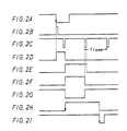
- a high potential signal is outputted from the exclusive OR gate G2 for the delayed time and applied to the other side input terminal of the AND gate G3 so that the AND gate G3 outputs high potential pulse signals as shown in Fig.
- the high potential pulse signals are inverted to low potential pulse signals at the inverter G4 and applied to a preset terminal ( PR ) of the flip-flop FF1 so that the flip-flop FF1 is preset and a high potential signal, as shown in Fig. 2D, is outputted from the output terminal Q1 and applied to an input terminal D2 of th flip- flop FF2.
- vertical synchronizing signals as shown in Fig. 2C are applied to the vertical synchronizing signal input terminal (VS), a low potential signal as shown in Fig. 2D is outputted from the output terminal Q1 of the flip-flop FF1 at the time that the vertical synchronizing signal is inputted first time, and at the same time a high potential signal as shown in Fig.
- the AND gate G5 accomplishes the AND operation of the signals as shown in Figs. 2C and 2E and outputs high potential signals for one frame period.
- the high potential signal outputted from the AND gate G5 is applied to one side input terminal of the AND gate G8 through the OR gate G10, and thereby the subcarrier frequency signal (fsc) is applied to the analog/digital converter 1 through the AND gate G8.
- video signals which are inputted to the video signal input terminal (Vi) are synchronized with the subcarrier frequency signal (fsc) at the analog/digital converter 1 and converted to digital signals, and then synchronized again with the subcarrier frequency signal (fsc) at the digital/analog converter 2 and converted to analog signals and outputted to a video signal output terminal (Vo).
- the high potential signal which is outputted from the AND gate G5 of the one-frame signal generating unit 5 is applied to a control terminal of the switch SW1 to short-circuit thereof and applied to the chip selecting terminal (cs) of the RAM31 to select thereof through the OR gate G11.
- the high potential signal is inverted into a low potential signal at the inverter G7 and applied to the write enable terminal ( WE ) of the RAM31 so that the RAM31 becomes to a writing-state. Accordingly, the signals which are outputted from the analog/digital converter 1 are stored in the RAM31 through the switch SW1.
- the high potential signal which is outputted from the AND gate G5 is inverted into a low potential signal, as shown in Fig. 2G, at the inverter G6 and applied to the clock terminal (CK) of the flip-flop FF3 so that a high potential signal, as shown in Fig. 2H, is outputted from the output terminal Q3 of the flip-flop FF3 and a low potential signal is outputted from the output terminal Q3 thereof. Thereafter, when a low potential signal, as shown in Fig.
- the switch SW1 since the low potential signal outputted from the AND gate G5 is applied to the control terminal of the switch SW1, the switch SW1 becomes to an open-state, and the low potential signal is inverted into a high potential signal at the inverter C7 and applied to a write enable terminal ( WE ) of the RAM31. And, the low potential signal outputted from the AND gate G5 is inverted into a high potential signal, as shown in Fig.
- digital signals stored in the RAM31 are read and pass through the switch SW2 and converted into analog signals at the digital/analog converter 2 by being synchronized with the subcarrier frequency signal (fsc) and then outputted to the video signal output terminal (Vo).
- a low potential signal as shown in Fig. 2I, is applied to the reset terminal ( RS ) of the flip-flop FF3, so that the flip-flop FF3 is reset and movie control signals are outputted therefrom. That is, since a low potential signal, as shown in Fig. 2H, is outputted from the output terminal Q3 of the flip-flop FF3, a low potential signal is outputted from the AND gate G9, thereby the RAM31 is not selected and the switch SW2 is opened.
Landscapes
- Engineering & Computer Science (AREA)
- Multimedia (AREA)
- Signal Processing (AREA)
- Television Signal Processing For Recording (AREA)
- Television Systems (AREA)
Applications Claiming Priority (2)
| Application Number | Priority Date | Filing Date | Title |
|---|---|---|---|
| KR2019890011264U KR930008445Y1 (ko) | 1989-07-31 | 1989-07-31 | 비디오폰용 정지 및 동작 화면 선택 제어회로 |
| KR1126489 | 1989-07-31 |
Publications (3)
| Publication Number | Publication Date |
|---|---|
| EP0411906A2 true EP0411906A2 (de) | 1991-02-06 |
| EP0411906A3 EP0411906A3 (en) | 1992-05-27 |
| EP0411906B1 EP0411906B1 (de) | 1997-10-01 |
Family
ID=19288769
Family Applications (1)
| Application Number | Title | Priority Date | Filing Date |
|---|---|---|---|
| EP90308420A Expired - Lifetime EP0411906B1 (de) | 1989-07-31 | 1990-07-31 | Steuerschaltung zur Auswahl Stehbild/Bewegtbild in einem Fernsehtelefonsystem |
Country Status (7)
| Country | Link |
|---|---|
| US (1) | US5063440A (de) |
| EP (1) | EP0411906B1 (de) |
| JP (1) | JP2558527Y2 (de) |
| KR (1) | KR930008445Y1 (de) |
| DE (1) | DE69031526T2 (de) |
| ES (1) | ES2108689T3 (de) |
| RU (1) | RU2121234C1 (de) |
Cited By (3)
| Publication number | Priority date | Publication date | Assignee | Title |
|---|---|---|---|---|
| EP0538013A3 (en) * | 1991-10-15 | 1993-10-27 | Sony Corp | Still image transmission system |
| US6356709B1 (en) | 1996-08-30 | 2002-03-12 | Sony Corporation | Device, method, and medium for recording still picture and animation |
| US9076073B2 (en) | 2013-06-06 | 2015-07-07 | Huawei Technologies Co., Ltd. | Photographing method, photo management method and device |
Families Citing this family (19)
| Publication number | Priority date | Publication date | Assignee | Title |
|---|---|---|---|---|
| US5283637A (en) * | 1990-08-20 | 1994-02-01 | Christine Holland Trustee/Goolcharan Trust | Telecommunication system for transmitting full motion video |
| US5587735A (en) * | 1991-07-24 | 1996-12-24 | Hitachi, Ltd. | Video telephone |
| EP0836323B1 (de) * | 1991-02-20 | 2004-01-14 | Hitachi, Ltd. | Bildfernsprechgerät |
| EP0523617B1 (de) * | 1991-07-15 | 1997-10-01 | Hitachi, Ltd. | Telekonferenzendstellengerät |
| EP0765083A1 (de) * | 1991-07-15 | 1997-03-26 | Hitachi, Ltd. | Telekonferenzendstellengerät |
| JPH0564185A (ja) * | 1991-08-29 | 1993-03-12 | Fujitsu Ltd | 多地点会議における2画面伝送表示方式 |
| US5357281A (en) * | 1991-11-07 | 1994-10-18 | Canon Kabushiki Kaisha | Image processing apparatus and terminal apparatus |
| US5751445A (en) * | 1991-11-11 | 1998-05-12 | Canon Kk | Image transmission system and terminal device |
| US5751722A (en) * | 1992-02-10 | 1998-05-12 | Canon Kabushiki Kaisha | Method of displaying a frozen image when transmission of image information is suspended in a multimedia system |
| US7624044B2 (en) | 1992-03-20 | 2009-11-24 | Stephen Wren | System for marketing goods and services utilizing computerized central and remote facilities |
| US5541640A (en) * | 1992-06-23 | 1996-07-30 | Larson; Craig R. | Videophone for simultaneous audio and video communication via a standard telephone line |
| DE4316168A1 (de) * | 1993-05-14 | 1994-11-17 | Sel Alcatel Ag | Bildanrufbeantworter |
| US5493329A (en) * | 1993-10-01 | 1996-02-20 | Toko Kabushiki Kaisha | Picture transmission system |
| CN1074220C (zh) * | 1994-01-31 | 2001-10-31 | 古卡伦信托 | 传送全活动图像的电信系统 |
| DE69738619T2 (de) * | 1996-07-23 | 2009-05-20 | Canon K.K. | Verfahren und Vorrichtung zur Kamerakontrolle |
| JP3862321B2 (ja) | 1996-07-23 | 2006-12-27 | キヤノン株式会社 | サーバ及びその制御方法 |
| JP3202606B2 (ja) * | 1996-07-23 | 2001-08-27 | キヤノン株式会社 | 撮像サーバ及びその方法及び媒体 |
| KR20040070559A (ko) * | 2003-02-04 | 2004-08-11 | 엘지전자 주식회사 | 복구 기능을 갖는 디스플레이 장치 및 그 방법 |
| US20090079744A1 (en) * | 2007-09-21 | 2009-03-26 | Microsoft Corporation | Animating objects using a declarative animation scheme |
Family Cites Families (10)
| Publication number | Priority date | Publication date | Assignee | Title |
|---|---|---|---|---|
| JPS5827716B2 (ja) * | 1973-07-31 | 1983-06-10 | ソニー株式会社 | ジキキロクソウチ |
| US4009330A (en) * | 1976-04-05 | 1977-02-22 | Bell Telephone Laboratories, Incorporated | Circuit for selecting frames indicative of still pictures |
| US4506387A (en) * | 1983-05-25 | 1985-03-19 | Walter Howard F | Programming-on-demand cable system and method |
| JPS61159883A (ja) * | 1985-01-08 | 1986-07-19 | Nippon Telegr & Teleph Corp <Ntt> | 狭帯域音声動画像送受信装置 |
| JP2650186B2 (ja) * | 1985-06-26 | 1997-09-03 | 三菱電機株式会社 | 静止画映像信号処理装置 |
| JPS62264781A (ja) * | 1986-05-12 | 1987-11-17 | Hitachi Ltd | 静止画記憶回路 |
| JPS63254875A (ja) * | 1987-04-10 | 1988-10-21 | Sony Corp | 画像モニタ−装置 |
| GB2211048A (en) * | 1987-06-26 | 1989-06-21 | Sony Corp | Video telephones |
| US4888795A (en) * | 1987-06-30 | 1989-12-19 | Nec Corporation | Videotelephone apparatus for transmitting high and low resolution video signals over telephone exchange lines |
| CA1318381C (en) * | 1988-04-15 | 1993-05-25 | Jun'ichi Ohki | Dual-mode teleconferencing system |
-
1989
- 1989-07-31 KR KR2019890011264U patent/KR930008445Y1/ko not_active Expired - Lifetime
-
1990
- 1990-07-30 US US07/559,165 patent/US5063440A/en not_active Expired - Lifetime
- 1990-07-31 DE DE69031526T patent/DE69031526T2/de not_active Expired - Fee Related
- 1990-07-31 ES ES90308420T patent/ES2108689T3/es not_active Expired - Lifetime
- 1990-07-31 JP JP1990080729U patent/JP2558527Y2/ja not_active Expired - Lifetime
- 1990-07-31 EP EP90308420A patent/EP0411906B1/de not_active Expired - Lifetime
- 1990-07-31 RU SU4830841A patent/RU2121234C1/ru active
Cited By (4)
| Publication number | Priority date | Publication date | Assignee | Title |
|---|---|---|---|---|
| EP0538013A3 (en) * | 1991-10-15 | 1993-10-27 | Sony Corp | Still image transmission system |
| US5691767A (en) * | 1991-10-15 | 1997-11-25 | Sony Corporation | Video conferencing system with high resolution still image capability |
| US6356709B1 (en) | 1996-08-30 | 2002-03-12 | Sony Corporation | Device, method, and medium for recording still picture and animation |
| US9076073B2 (en) | 2013-06-06 | 2015-07-07 | Huawei Technologies Co., Ltd. | Photographing method, photo management method and device |
Also Published As
| Publication number | Publication date |
|---|---|
| ES2108689T3 (es) | 1998-01-01 |
| EP0411906B1 (de) | 1997-10-01 |
| JPH0356270U (de) | 1991-05-30 |
| KR930008445Y1 (ko) | 1993-12-22 |
| DE69031526T2 (de) | 1998-02-19 |
| EP0411906A3 (en) | 1992-05-27 |
| JP2558527Y2 (ja) | 1997-12-24 |
| KR910003664U (ko) | 1991-02-27 |
| DE69031526D1 (de) | 1997-11-06 |
| RU2121234C1 (ru) | 1998-10-27 |
| US5063440A (en) | 1991-11-05 |
Similar Documents
| Publication | Publication Date | Title |
|---|---|---|
| EP0411906A2 (de) | Steuerschaltung zur Auswahl Stehbild/Bewegtbild in einem Fernsehtelefonsystem | |
| US6184930B1 (en) | Electronic still camera with dual contact shutter switch for picture review | |
| US5497194A (en) | Electronic camera for photographing and recording an image and for recording and reproducing a voice | |
| JPH01191581A (ja) | タイトル画像挿入装置 | |
| EP0467683A2 (de) | Bildverarbeitungsgerät | |
| CA1108287A (en) | Special video effect generator | |
| JPS61293077A (ja) | 撮像装置 | |
| US4901148A (en) | Data processing device | |
| EP0637169B1 (de) | Zeichensignalanzeige für einen Camcorder | |
| KR930010844B1 (ko) | 전자카메라의 비디오신호기록장치 | |
| JPS6154774A (ja) | テレビジヨン同期信号波形処理装置 | |
| JPH0630369A (ja) | 遅延画像データ出力ビデオカメラ | |
| JP3298105B2 (ja) | クランプ回路 | |
| JPS63260376A (ja) | カメラ一体型ビデオレコ−ダ | |
| JPH01196981A (ja) | タイトル画像挿入装置 | |
| JPH02214271A (ja) | 記録装置 | |
| JPS60261265A (ja) | 映像信号記録装置 | |
| KR930012244B1 (ko) | 디지탈스틸비디오카메라의메세지기록/재생회로및그방식 | |
| JP3182176B2 (ja) | カメラ一体型ビデオテープレコーダ | |
| JP2943546B2 (ja) | 画像記憶回路及びこれを用いた映像処理装置 | |
| JPS6018074A (ja) | フイ−ルド信号処理回路 | |
| JPH0510465Y2 (de) | ||
| JPH0411472A (ja) | タイトル画像挿入装置 | |
| JPS63181578A (ja) | 映像記憶装置 | |
| JPH06165030A (ja) | 映像信号切換回路 |
Legal Events
| Date | Code | Title | Description |
|---|---|---|---|
| PUAI | Public reference made under article 153(3) epc to a published international application that has entered the european phase |
Free format text: ORIGINAL CODE: 0009012 |
|
| AK | Designated contracting states |
Kind code of ref document: A2 Designated state(s): DE ES FR GB IT |
|
| PUAL | Search report despatched |
Free format text: ORIGINAL CODE: 0009013 |
|
| AK | Designated contracting states |
Kind code of ref document: A3 Designated state(s): DE ES FR GB IT |
|
| 17P | Request for examination filed |
Effective date: 19921019 |
|
| 17Q | First examination report despatched |
Effective date: 19940829 |
|
| GRAG | Despatch of communication of intention to grant |
Free format text: ORIGINAL CODE: EPIDOS AGRA |
|
| GRAH | Despatch of communication of intention to grant a patent |
Free format text: ORIGINAL CODE: EPIDOS IGRA |
|
| GRAH | Despatch of communication of intention to grant a patent |
Free format text: ORIGINAL CODE: EPIDOS IGRA |
|
| GRAA | (expected) grant |
Free format text: ORIGINAL CODE: 0009210 |
|
| AK | Designated contracting states |
Kind code of ref document: B1 Designated state(s): DE ES FR GB IT |
|
| ITF | It: translation for a ep patent filed | ||
| REF | Corresponds to: |
Ref document number: 69031526 Country of ref document: DE Date of ref document: 19971106 |
|
| REG | Reference to a national code |
Ref country code: ES Ref legal event code: FG2A Ref document number: 2108689 Country of ref document: ES Kind code of ref document: T3 |
|
| ET | Fr: translation filed | ||
| PLBE | No opposition filed within time limit |
Free format text: ORIGINAL CODE: 0009261 |
|
| STAA | Information on the status of an ep patent application or granted ep patent |
Free format text: STATUS: NO OPPOSITION FILED WITHIN TIME LIMIT |
|
| 26N | No opposition filed | ||
| REG | Reference to a national code |
Ref country code: GB Ref legal event code: IF02 |
|
| PGFP | Annual fee paid to national office [announced via postgrant information from national office to epo] |
Ref country code: ES Payment date: 20050818 Year of fee payment: 16 |
|
| REG | Reference to a national code |
Ref country code: FR Ref legal event code: FC |
|
| PGFP | Annual fee paid to national office [announced via postgrant information from national office to epo] |
Ref country code: FR Payment date: 20060719 Year of fee payment: 17 |
|
| PGFP | Annual fee paid to national office [announced via postgrant information from national office to epo] |
Ref country code: GB Payment date: 20060726 Year of fee payment: 17 |
|
| PGFP | Annual fee paid to national office [announced via postgrant information from national office to epo] |
Ref country code: DE Payment date: 20060727 Year of fee payment: 17 |
|
| PGFP | Annual fee paid to national office [announced via postgrant information from national office to epo] |
Ref country code: IT Payment date: 20060731 Year of fee payment: 17 |
|
| GBPC | Gb: european patent ceased through non-payment of renewal fee |
Effective date: 20070731 |
|
| PG25 | Lapsed in a contracting state [announced via postgrant information from national office to epo] |
Ref country code: DE Free format text: LAPSE BECAUSE OF NON-PAYMENT OF DUE FEES Effective date: 20080201 |
|
| PG25 | Lapsed in a contracting state [announced via postgrant information from national office to epo] |
Ref country code: GB Free format text: LAPSE BECAUSE OF NON-PAYMENT OF DUE FEES Effective date: 20070731 |
|
| REG | Reference to a national code |
Ref country code: FR Ref legal event code: ST Effective date: 20080331 |
|
| PG25 | Lapsed in a contracting state [announced via postgrant information from national office to epo] |
Ref country code: FR Free format text: LAPSE BECAUSE OF NON-PAYMENT OF DUE FEES Effective date: 20070731 |
|
| REG | Reference to a national code |
Ref country code: ES Ref legal event code: FD2A Effective date: 20070801 |
|
| PG25 | Lapsed in a contracting state [announced via postgrant information from national office to epo] |
Ref country code: ES Free format text: LAPSE BECAUSE OF NON-PAYMENT OF DUE FEES Effective date: 20070801 |
|
| PG25 | Lapsed in a contracting state [announced via postgrant information from national office to epo] |
Ref country code: IT Free format text: LAPSE BECAUSE OF NON-PAYMENT OF DUE FEES Effective date: 20070731 |
|
| REG | Reference to a national code |
Ref legal event code: ER Free format text: IN BULETIN 05/46 (20051012) CONCERNEE 6.1 DECISION DU DIRECTEUR GENERAL STATUANT FAVORABLEMENT SUR UN RECOURS. IL Y A REMPLACER CE BREVET EUROPEEN PAR LA BREVET FRANCAIS NO 0411906 Ref country code: FR |