EP0411914A2 - Tête magnétique en films minces - Google Patents
Tête magnétique en films minces Download PDFInfo
- Publication number
- EP0411914A2 EP0411914A2 EP90308445A EP90308445A EP0411914A2 EP 0411914 A2 EP0411914 A2 EP 0411914A2 EP 90308445 A EP90308445 A EP 90308445A EP 90308445 A EP90308445 A EP 90308445A EP 0411914 A2 EP0411914 A2 EP 0411914A2
- Authority
- EP
- European Patent Office
- Prior art keywords
- yoke
- magnetic
- thin film
- recording
- yokes
- Prior art date
- Legal status (The legal status is an assumption and is not a legal conclusion. Google has not performed a legal analysis and makes no representation as to the accuracy of the status listed.)
- Granted
Links
Images


Classifications
-
- G—PHYSICS
- G11—INFORMATION STORAGE
- G11B—INFORMATION STORAGE BASED ON RELATIVE MOVEMENT BETWEEN RECORD CARRIER AND TRANSDUCER
- G11B5/00—Recording by magnetisation or demagnetisation of a record carrier; Reproducing by magnetic means; Record carriers therefor
- G11B5/127—Structure or manufacture of heads, e.g. inductive
- G11B5/31—Structure or manufacture of heads, e.g. inductive using thin films
-
- G—PHYSICS
- G11—INFORMATION STORAGE
- G11B—INFORMATION STORAGE BASED ON RELATIVE MOVEMENT BETWEEN RECORD CARRIER AND TRANSDUCER
- G11B5/00—Recording by magnetisation or demagnetisation of a record carrier; Reproducing by magnetic means; Record carriers therefor
- G11B5/127—Structure or manufacture of heads, e.g. inductive
- G11B5/33—Structure or manufacture of flux-sensitive heads, i.e. for reproduction only; Combination of such heads with means for recording or erasing only
- G11B5/39—Structure or manufacture of flux-sensitive heads, i.e. for reproduction only; Combination of such heads with means for recording or erasing only using magneto-resistive devices or effects
- G11B5/3903—Structure or manufacture of flux-sensitive heads, i.e. for reproduction only; Combination of such heads with means for recording or erasing only using magneto-resistive devices or effects using magnetic thin film layers or their effects, the films being part of integrated structures
- G11B5/3906—Details related to the use of magnetic thin film layers or to their effects
- G11B5/3916—Arrangements in which the active read-out elements are coupled to the magnetic flux of the track by at least one magnetic thin film flux guide
- G11B5/3919—Arrangements in which the active read-out elements are coupled to the magnetic flux of the track by at least one magnetic thin film flux guide the guide being interposed in the flux path
- G11B5/3922—Arrangements in which the active read-out elements are coupled to the magnetic flux of the track by at least one magnetic thin film flux guide the guide being interposed in the flux path the read-out elements being disposed in magnetic shunt relative to at least two parts of the flux guide structure
- G11B5/3925—Arrangements in which the active read-out elements are coupled to the magnetic flux of the track by at least one magnetic thin film flux guide the guide being interposed in the flux path the read-out elements being disposed in magnetic shunt relative to at least two parts of the flux guide structure the two parts being thin films
-
- G—PHYSICS
- G11—INFORMATION STORAGE
- G11B—INFORMATION STORAGE BASED ON RELATIVE MOVEMENT BETWEEN RECORD CARRIER AND TRANSDUCER
- G11B5/00—Recording by magnetisation or demagnetisation of a record carrier; Reproducing by magnetic means; Record carriers therefor
- G11B5/127—Structure or manufacture of heads, e.g. inductive
- G11B5/187—Structure or manufacture of the surface of the head in physical contact with, or immediately adjacent to the recording medium; Pole pieces; Gap features
- G11B5/245—Structure or manufacture of the surface of the head in physical contact with, or immediately adjacent to the recording medium; Pole pieces; Gap features comprising means for controlling the reluctance of the magnetic circuit in a head with single gap, for co-operation with one track
- G11B5/2452—Structure or manufacture of the surface of the head in physical contact with, or immediately adjacent to the recording medium; Pole pieces; Gap features comprising means for controlling the reluctance of the magnetic circuit in a head with single gap, for co-operation with one track where the dimensions of the effective gap are controlled
-
- G—PHYSICS
- G11—INFORMATION STORAGE
- G11B—INFORMATION STORAGE BASED ON RELATIVE MOVEMENT BETWEEN RECORD CARRIER AND TRANSDUCER
- G11B5/00—Recording by magnetisation or demagnetisation of a record carrier; Reproducing by magnetic means; Record carriers therefor
- G11B5/127—Structure or manufacture of heads, e.g. inductive
- G11B5/31—Structure or manufacture of heads, e.g. inductive using thin films
- G11B5/3109—Details
- G11B5/3116—Shaping of layers, poles or gaps for improving the form of the electrical signal transduced, e.g. for shielding, contour effect, equalizing, side flux fringing, cross talk reduction between heads or between heads and information tracks
-
- G—PHYSICS
- G11—INFORMATION STORAGE
- G11B—INFORMATION STORAGE BASED ON RELATIVE MOVEMENT BETWEEN RECORD CARRIER AND TRANSDUCER
- G11B5/00—Recording by magnetisation or demagnetisation of a record carrier; Reproducing by magnetic means; Record carriers therefor
- G11B5/127—Structure or manufacture of heads, e.g. inductive
- G11B5/33—Structure or manufacture of flux-sensitive heads, i.e. for reproduction only; Combination of such heads with means for recording or erasing only
- G11B5/39—Structure or manufacture of flux-sensitive heads, i.e. for reproduction only; Combination of such heads with means for recording or erasing only using magneto-resistive devices or effects
- G11B5/3903—Structure or manufacture of flux-sensitive heads, i.e. for reproduction only; Combination of such heads with means for recording or erasing only using magneto-resistive devices or effects using magnetic thin film layers or their effects, the films being part of integrated structures
- G11B5/3906—Details related to the use of magnetic thin film layers or to their effects
- G11B5/3945—Heads comprising more than one sensitive element
-
- G—PHYSICS
- G11—INFORMATION STORAGE
- G11B—INFORMATION STORAGE BASED ON RELATIVE MOVEMENT BETWEEN RECORD CARRIER AND TRANSDUCER
- G11B5/00—Recording by magnetisation or demagnetisation of a record carrier; Reproducing by magnetic means; Record carriers therefor
- G11B5/127—Structure or manufacture of heads, e.g. inductive
- G11B5/33—Structure or manufacture of flux-sensitive heads, i.e. for reproduction only; Combination of such heads with means for recording or erasing only
- G11B5/39—Structure or manufacture of flux-sensitive heads, i.e. for reproduction only; Combination of such heads with means for recording or erasing only using magneto-resistive devices or effects
- G11B5/3903—Structure or manufacture of flux-sensitive heads, i.e. for reproduction only; Combination of such heads with means for recording or erasing only using magneto-resistive devices or effects using magnetic thin film layers or their effects, the films being part of integrated structures
- G11B5/3967—Composite structural arrangements of transducers, e.g. inductive write and magnetoresistive read
Definitions
- the present invention relates to a thin film magnetic head for use with magnetic recording apparatuses, and, more particularly, to a thin film magnetic head in which a recording head and a reproducing head are formed integral with each other.
- a prior inductive head produces a reproducing output proportional to running speeds of a recording medium.
- a thin film magnetic head using the magnetoresistance effect is not dependent upon a relative speed between the head and a recording medium and produces a constant reproducing output such that the output is not reduced even when such relative speed is small. Accordingly, this type of this film magnetic heads have been widely used with magnetic recording apparatuses in recent years. However, since such thin film magnetoresistive head is not capable of recording, it must be combined with an inductive thin film head of coil type in order to provide both recording and reproducing functions. An example of such thin film magnetic head is disclosed in Japanese Patent Unexamined Publication Nos. 52-12814 and 61-48116.
- lower and upper magnetic layers are linearly extended in opposed relationship with each other on a substrate, and these magnetic layers and a magnetic gap formed therebetween constitute a magnetic circuit.
- a coil layer is formed around the magnetic circuit.
- the upper magnetic layer is divided into front and rear sections, and a magnetoresistive element is arranged to bridge these sections.
- This thin film magnetic head acts in the manner described hereinbelow.
- a recording current flows through the coil layer, so that a recording magnetic field leaks to the outside through the magnetic gap, writing on a recording medium is performed by the thus leaking magnetic field.
- a signal magnetic flux generated from the recorded medium passes through the magnetic gap and the front section of the upper magnetic layer to flow into the magnetoresistive element.
- the signal is detected from the resistance change of the magnetoresistive element. More specifically, a sense current is applied to the magnetoresistive element and the resistance change of the element is transformed into a voltage change such that the signal is read out.
- Such prior thin film magnetic head can not provide favorable recording and reproducing in case the recording medium is not good in the running accuracy because the track width is the same in recording and reproducing. More specifically, assuming that the prior thin film magnetic head has a recording and reproducing track width T1 and the recording medium has a running accuracy of ⁇ a, the maximum running deviation in recording and reproducing will become 2a and the effective reproducing track width will become T1 - 2a,
- the invention provides a thin film magnetic head in which an upper magnetic layer comprises a first yoke having a portion thereof substituted by a magnetoresistive element and a second yoke provided adjacent the first yoke, said first and second yokes defining a recording track width.
- the first and second yokes can be mainly used to wide-record on the recording medium, and only the first yoke can be used to narrow-reproduce on the recording medium, so that the reproducing output is not reduced when the recording medium experiences a running deviation.
- a thin film magnetic head includes a nonmagnetic substrate 1 made of ceramics, glass or the like, a lower magnetic layer 2 formed of a soft magnetic material such as permalloy, sendust or the like by sputtering process and provided on the nonmagnetic substrate 1 to have the same width as that of a recording track, a gap layer 3 made of an insulating material (SiO2) and provided on the lower magnetic layer 2, a conductor coil 4 formed on an insulating layer 10, a magnetoresistive element 5 made of a nickel-iron alloy and provided on the insulating layer 10, and first and second yokes 6 and 7 each made from permalloy or sendust by sputtering and divided into front and rear sections.
- a nonmagnetic substrate 1 made of ceramics, glass or the like
- a lower magnetic layer 2 formed of a soft magnetic material such as permalloy, sendust or the like by sputtering process and provided on the nonmagnetic substrate 1 to have the same width as
- the first yoke 6, magenetroresistive element 5, gap layer 3 and the lower magnetic layer 2 cooperate to form a magnetic circuit which surrounds the conductor coil 4.
- the second yoke 7 is arranged at positions spaced by a distance X in the widthwise direction of the recording track.
- a third yoke 28 Provided contiguous to the first and second yokes is a third yoke 28 which is positioned therebetween so as to be contacted by the recording medium and has a larger magnetic reluctance than those of the first and second yokes 6 and 7.
- the second and third yokes cooperate with the gap layer 3 and the lower magnetic layer 2 to form a magnetic circuit which surrounds the conductor coil 4.
- electrodes 8 for reproducing only a signal magnetic field which is generated from the recording medium by the first yoke 6.
- a recording current is applied to the conductor coil 4, and the induced magnetic field for recording is generated to the gap layer 3 through the magnetic circuit comprising the first yoke 6 and the lower magnetic layer 2 and through the magnetic circuit comprising the second yoke 7 and the lower magnetic layer 2 so that recording is effected on the recording medium.
- the magnetic field for recording flows into the third yoke 28.
- the width Tw of the recording track is the sum of the widths of the first, second and third yokes.
- the magnetic field from the recording medium is conducted mainly through the first and second yokes 6 and 7.
- the third yoke 28 is provided between the first and second yokes 6 and 7 and the magnetic reluctance of the third yoke 28 is larger than those of the first and second yokes, the magnetic field conducted through the second yoke 7 will not flow into the magnetoresistive element 5, so that the width of the first yoke 6 substantially defines a width of the reproducing track.
- the thin film magnetic head is constructed such that the recording track width Tw and the reproducing track width Tr make Tw ⁇ Tr + 2a, so that even when the running deviation of the recording medium becomes 2a at maximum in recording and reproducing, the reproducing track is included within the recording track to prevent the reproducing signal output from being lowered.
- the signal magnetic field in the adjacent track flows into the yoke 7, but will not flow into the magnetoresistive element 5 since the third yoke is provided between the second yoke 7 and the first yoke 6 and has a larger magnetic reluctance than those of the first and second yokes. Accordingly, a good reproducing with little cross talk can be obtained.
- a second embodiment of the invention will be described hereinbelow.
- the same parts as those shown in Figs. 1A to 1C are designated by the same reference numerals, and the explanation thereof is omitted.
- the second embodiment is different from the first embodiment in that a second yoke 17 is divided into front and rear sections, like the first yoke 6.
- the magnetic circuit comprising the lower magnetic layer 2 and the first yoke 6 and the magnetic circuit comprising the lower magnetic layer 2 and the second yoke 17 are substantially identical to each other in constitution.
- a magnetic field generated by applying a recording current to the conductor coil 4 passes through the magnetic circuit comprising the lower magnetic layer 2 and the first yoke 6 and the magnetic circuit comprising the lower magnetic layer 2 and the second yoke 7 to reach the respective magnetic gaps, thus generating recording magnetic fields of substantially the same strength. Accordingly, dispersion in the quality of recording over the recording medium is reduced. To improve such effect, dummy magnetoresistive elements may be provided on the divided sections of the second yoke 17.
- Figs. 3A to 3C show a third embodiment of the invention.
- the same parts as those of the first and second embodiments are designated by the same reference numerals.
- a third yoke 18 is formed to have a thinner film thickness and a larger magnetic reluctance than those of the first yoke 6 and the second yoke 17.
- the third embodiment operates in substantially the same manner as the first and second embodiments, thus providing substantially the same effect as that of the preceding embodiments.
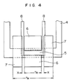
- Fig. 4 shows a plan view of a thin film magnetic head according to a fourth embodiment of the invention, in which the second yoke 7 is arranged at the positions laterally spaced by a distance X from the opposite ends of the first yoke 6.
- the recording track width Tw is the sum of the widths of the first yoke 6, second yoke 7 and the distances X of the gaps between the first yoke 6 and the second yoke 7.
- the width of the reproducing track corresponds to the width T R of the first yoke 6.
- the distance X is sufficiently small as compared with the width T R of the first yoke 6, the reproducing output is little affected by such running deviations. Accordingly, favorable recording and reproducing can be effected.
- the second yoke 6 may be divided into front and rear sections in a similar manner to the second embodiment.
- the recording track width is defined with the upper and lower magnetic layers set at the same width in all of the embodiments, the upper and lower magnetic layers having different widths to provide a magnetic layer of a small width may define the width of the recording track.
Landscapes
- Engineering & Computer Science (AREA)
- Manufacturing & Machinery (AREA)
- Magnetic Heads (AREA)
Applications Claiming Priority (4)
| Application Number | Priority Date | Filing Date | Title |
|---|---|---|---|
| JP1203259A JP2563596B2 (ja) | 1989-08-04 | 1989-08-04 | 複合型薄膜磁気ヘッド |
| JP203258/89 | 1989-08-04 | ||
| JP203259/89 | 1989-08-04 | ||
| JP1203258A JP2563595B2 (ja) | 1989-08-04 | 1989-08-04 | 複合型薄膜磁気ヘッド |
Publications (3)
| Publication Number | Publication Date |
|---|---|
| EP0411914A2 true EP0411914A2 (fr) | 1991-02-06 |
| EP0411914A3 EP0411914A3 (en) | 1991-10-16 |
| EP0411914B1 EP0411914B1 (fr) | 1996-03-13 |
Family
ID=26513827
Family Applications (1)
| Application Number | Title | Priority Date | Filing Date |
|---|---|---|---|
| EP90308445A Expired - Lifetime EP0411914B1 (fr) | 1989-08-04 | 1990-07-31 | Tête magnétique en films minces |
Country Status (4)
| Country | Link |
|---|---|
| US (1) | US5097372A (fr) |
| EP (1) | EP0411914B1 (fr) |
| KR (1) | KR940004989B1 (fr) |
| DE (1) | DE69025820T2 (fr) |
Cited By (7)
| Publication number | Priority date | Publication date | Assignee | Title |
|---|---|---|---|---|
| EP0467457A1 (fr) * | 1990-07-18 | 1992-01-22 | Koninklijke Philips Electronics N.V. | Tête magnétique à film mince |
| EP0669608A1 (fr) * | 1994-02-18 | 1995-08-30 | Hewlett-Packard Company | Tête planaire à entrefer de lecture et d'écriture séparés |
| EP0638893A3 (fr) * | 1993-08-10 | 1996-05-15 | Read Rite Corp | Tête magnétique avec élément détecteur de flux pour enregistrer/reproduire sur une bande. |
| EP0616318A3 (en) * | 1993-03-18 | 1997-02-26 | Fujitsu Ltd | Magnetoresistive head. |
| EP0675486A3 (fr) * | 1994-03-31 | 1997-02-26 | Read Rite Corp | Transducteur magnétorésistif à culasse intégrée et dérivation magnétique. |
| US5995339A (en) * | 1993-03-18 | 1999-11-30 | Fujitsu Limited | Magnetoresistive head with a front flux guide and an embedded MR element |
| SG90755A1 (en) * | 1999-10-13 | 2002-08-20 | Sony Corp | Magnetoresistive effect magnetic head and rotary magnetic head apparatus |
Families Citing this family (14)
| Publication number | Priority date | Publication date | Assignee | Title |
|---|---|---|---|---|
| NL9000546A (nl) * | 1990-03-09 | 1991-10-01 | Philips Nv | Werkwijze voor het vervaardigen van een dunnefilm magneetkop alsmede een dunnefilm magneetkop vervaardigbaar volgens de werkwijze. |
| JPH0434713A (ja) * | 1990-05-30 | 1992-02-05 | Sony Corp | 磁気抵抗効果型薄膜ヘッド |
| EP0478256B1 (fr) * | 1990-09-27 | 1997-05-14 | Kabushiki Kaisha Toshiba | Tête magnétique |
| JP2687258B2 (ja) * | 1991-04-26 | 1997-12-08 | キヤノン株式会社 | 情報記録部を備えたフィルムに対して使用されるヘッド装置及び情報記録部を備えたフィルムを使用する装置 |
| US5269895A (en) * | 1991-05-21 | 1993-12-14 | North American Philips Corporation | Method of making composite structure with single domain magnetic element |
| JP3022023B2 (ja) * | 1992-04-13 | 2000-03-15 | 株式会社日立製作所 | 磁気記録再生装置 |
| US6078479A (en) * | 1993-08-10 | 2000-06-20 | Read-Rite Corporation | Magnetic tape head with flux sensing element |
| JP2780916B2 (ja) * | 1993-12-08 | 1998-07-30 | 富士通株式会社 | 垂直磁気記録用磁気ヘッド |
| US6005751A (en) * | 1994-01-28 | 1999-12-21 | Seagate Technology, Inc. | Recording head skewed read gap/write gap positioning |
| US5604651A (en) * | 1994-02-23 | 1997-02-18 | Applied Magentics Corporation | Read head with 4-point magnetoresistive sensing |
| US5502522A (en) * | 1994-05-12 | 1996-03-26 | Eastman Kodak Company | Compact magnetic head for a photographic camera |
| US5493467A (en) * | 1994-12-27 | 1996-02-20 | International Business Machines Corporation | Yoke spin valve MR read head |
| US5982177A (en) * | 1997-08-08 | 1999-11-09 | Florida State University | Magnetoresistive sensor magnetically biased in a region spaced from a sensing region |
| JP4202958B2 (ja) * | 2004-03-30 | 2008-12-24 | 株式会社東芝 | 磁気抵抗効果素子 |
Family Cites Families (20)
| Publication number | Priority date | Publication date | Assignee | Title |
|---|---|---|---|---|
| GB1344890A (en) * | 1971-08-21 | 1974-01-23 | Ibm | Electromagnetic transducers |
| US4566050A (en) * | 1982-12-30 | 1986-01-21 | International Business Machines Corp. (Ibm) | Skew insensitive magnetic read head |
| JPS6050612A (ja) * | 1983-08-29 | 1985-03-20 | Sony Corp | 磁気抵抗効果型磁気ヘツド |
| DE3340600C1 (de) * | 1983-11-10 | 1985-01-10 | Doduco KG Dr. Eugen Dürrwächter, 7530 Pforzheim | Lesekopf zum magnetischen Abtasten von Wiegand-Draehten |
| JPS61196418A (ja) * | 1985-02-25 | 1986-08-30 | Matsushita Electric Ind Co Ltd | 薄膜磁気ヘツド |
| US4802043A (en) * | 1985-03-25 | 1989-01-31 | Hitachi, Ltd. | Magneto-resistive head for protecting against output spike noises |
| DE3613619A1 (de) * | 1985-04-26 | 1986-10-30 | Sharp K.K., Osaka | Duennfilm-magnetkopf |
| JPS61276110A (ja) * | 1985-05-30 | 1986-12-06 | Nec Corp | 磁気抵抗効果型磁気ヘツド |
| JPS6243813A (ja) * | 1985-08-20 | 1987-02-25 | Seiko Epson Corp | 磁気ヘツド |
| JPS6292215A (ja) * | 1985-10-18 | 1987-04-27 | Seiko Epson Corp | 磁気ヘツド |
| JPH0831204B2 (ja) * | 1985-10-18 | 1996-03-27 | 富士通株式会社 | 薄膜磁気ヘツド |
| EP0269129B1 (fr) * | 1986-11-28 | 1993-09-22 | Nec Corporation | Tête magnétique à films minces |
| US4885649A (en) * | 1987-04-01 | 1989-12-05 | Digital Equipment Corporation | Thin film head having a magneto-restrictive read element |
| US4935832A (en) * | 1987-04-01 | 1990-06-19 | Digital Equipment Corporation | Recording heads with side shields |
| AU1628188A (en) * | 1987-04-01 | 1988-11-02 | Digital Equipment Corporation | Magneto-resistive thin film head for digital magnetic storage device |
| US4816947A (en) * | 1987-11-12 | 1989-03-28 | International Business Machines | Single track vertical and horizontal recording read/write head design |
| JPH01138608A (ja) * | 1987-11-26 | 1989-05-31 | Matsushita Electric Ind Co Ltd | Mrヘッド |
| US4881143A (en) * | 1988-01-19 | 1989-11-14 | Hewlett-Packard Company | Compensated magneto-resistive read head |
| JPH01307008A (ja) * | 1988-06-03 | 1989-12-12 | Hitachi Ltd | 薄膜磁気ヘツド |
| JPH02105307A (ja) * | 1988-10-14 | 1990-04-17 | Sumitomo Metal Ind Ltd | 薄膜磁気ヘッドの製造方法 |
-
1990
- 1990-07-30 KR KR1019900011601A patent/KR940004989B1/ko not_active Expired - Fee Related
- 1990-07-30 US US07/559,067 patent/US5097372A/en not_active Expired - Fee Related
- 1990-07-31 DE DE69025820T patent/DE69025820T2/de not_active Expired - Fee Related
- 1990-07-31 EP EP90308445A patent/EP0411914B1/fr not_active Expired - Lifetime
Cited By (8)
| Publication number | Priority date | Publication date | Assignee | Title |
|---|---|---|---|---|
| EP0467457A1 (fr) * | 1990-07-18 | 1992-01-22 | Koninklijke Philips Electronics N.V. | Tête magnétique à film mince |
| US5247412A (en) * | 1990-07-18 | 1993-09-21 | U.S. Philips Corporation | Thin-film magnetic head |
| EP0616318A3 (en) * | 1993-03-18 | 1997-02-26 | Fujitsu Ltd | Magnetoresistive head. |
| US5995339A (en) * | 1993-03-18 | 1999-11-30 | Fujitsu Limited | Magnetoresistive head with a front flux guide and an embedded MR element |
| EP0638893A3 (fr) * | 1993-08-10 | 1996-05-15 | Read Rite Corp | Tête magnétique avec élément détecteur de flux pour enregistrer/reproduire sur une bande. |
| EP0669608A1 (fr) * | 1994-02-18 | 1995-08-30 | Hewlett-Packard Company | Tête planaire à entrefer de lecture et d'écriture séparés |
| EP0675486A3 (fr) * | 1994-03-31 | 1997-02-26 | Read Rite Corp | Transducteur magnétorésistif à culasse intégrée et dérivation magnétique. |
| SG90755A1 (en) * | 1999-10-13 | 2002-08-20 | Sony Corp | Magnetoresistive effect magnetic head and rotary magnetic head apparatus |
Also Published As
| Publication number | Publication date |
|---|---|
| DE69025820T2 (de) | 1996-10-02 |
| US5097372A (en) | 1992-03-17 |
| KR940004989B1 (ko) | 1994-06-09 |
| EP0411914A3 (en) | 1991-10-16 |
| DE69025820D1 (de) | 1996-04-18 |
| EP0411914B1 (fr) | 1996-03-13 |
| KR910005235A (ko) | 1991-03-30 |
Similar Documents
| Publication | Publication Date | Title |
|---|---|---|
| US5097372A (en) | Thin film magnetic head with wide recording area and narrow reproducing area | |
| EP0472187B1 (fr) | Tête magnétique plane avec film mince | |
| US5434733A (en) | Planar head having separate read and write gaps | |
| US5402292A (en) | Magnetoresistance effect type thin film magnetic head using high coercion films | |
| US5095397A (en) | Thin film magnetic head of embodied recording and reproducing transducer type | |
| EP0521564B1 (fr) | Tête magnétique à films minces | |
| EP0204902A2 (fr) | Tête de transducteur magnétique du type à culasse utilisant un effet magnétorésistif | |
| US5754376A (en) | Magnetoresistive head with hard magnetic bias | |
| US6191925B1 (en) | Dual element read with shaped elements | |
| EP0675486A2 (fr) | Transducteur magnétorésistif à culasse intégrée et dérivation magnétique | |
| EP0111755B1 (fr) | Transducteur magnétique à double élément | |
| JPS61107520A (ja) | 多チヤンネル磁気抵抗効果型磁気ヘツド | |
| EP0702357B1 (fr) | Tête à effet de magnétorésistance et tête d'enregistrement/reproduction magnétique en découlant | |
| US20020036875A1 (en) | Magnetoresistive head | |
| EP0514976B1 (fr) | Tête magnétique combinée de lecture/écriture | |
| KR100267411B1 (ko) | 자기 저항 헤드 | |
| EP0553434B1 (fr) | Tête magnétique à films minces | |
| EP0613120B1 (fr) | Tête magnétique à film mince, à magnétorésistance | |
| US4821012A (en) | Magnetoresistive element | |
| KR100488638B1 (ko) | 자기저항소자를구비한단일채널자기헤드 | |
| US5774309A (en) | Magnetic transducer and thin film magnetic head | |
| JPH05166137A (ja) | 磁気ヘッドおよび記録再生装置 | |
| JPH05266437A (ja) | 磁気抵抗効果型ヘッド | |
| JPS61177616A (ja) | 薄膜磁気ヘツド | |
| JPH06223333A (ja) | 磁気抵抗効果再生ヘッド |
Legal Events
| Date | Code | Title | Description |
|---|---|---|---|
| PUAI | Public reference made under article 153(3) epc to a published international application that has entered the european phase |
Free format text: ORIGINAL CODE: 0009012 |
|
| AK | Designated contracting states |
Kind code of ref document: A2 Designated state(s): DE FR GB |
|
| 17P | Request for examination filed |
Effective date: 19901228 |
|
| PUAL | Search report despatched |
Free format text: ORIGINAL CODE: 0009013 |
|
| AK | Designated contracting states |
Kind code of ref document: A3 Designated state(s): DE FR GB |
|
| 17Q | First examination report despatched |
Effective date: 19931203 |
|
| GRAH | Despatch of communication of intention to grant a patent |
Free format text: ORIGINAL CODE: EPIDOS IGRA |
|
| GRAA | (expected) grant |
Free format text: ORIGINAL CODE: 0009210 |
|
| AK | Designated contracting states |
Kind code of ref document: B1 Designated state(s): DE FR GB |
|
| REF | Corresponds to: |
Ref document number: 69025820 Country of ref document: DE Date of ref document: 19960418 |
|
| ET | Fr: translation filed | ||
| PLBE | No opposition filed within time limit |
Free format text: ORIGINAL CODE: 0009261 |
|
| STAA | Information on the status of an ep patent application or granted ep patent |
Free format text: STATUS: NO OPPOSITION FILED WITHIN TIME LIMIT |
|
| 26N | No opposition filed | ||
| PGFP | Annual fee paid to national office [announced via postgrant information from national office to epo] |
Ref country code: FR Payment date: 20000711 Year of fee payment: 11 |
|
| PGFP | Annual fee paid to national office [announced via postgrant information from national office to epo] |
Ref country code: GB Payment date: 20000726 Year of fee payment: 11 |
|
| PGFP | Annual fee paid to national office [announced via postgrant information from national office to epo] |
Ref country code: DE Payment date: 20000729 Year of fee payment: 11 |
|
| PG25 | Lapsed in a contracting state [announced via postgrant information from national office to epo] |
Ref country code: GB Free format text: LAPSE BECAUSE OF NON-PAYMENT OF DUE FEES Effective date: 20010731 |
|
| GBPC | Gb: european patent ceased through non-payment of renewal fee |
Effective date: 20010731 |
|
| PG25 | Lapsed in a contracting state [announced via postgrant information from national office to epo] |
Ref country code: FR Free format text: LAPSE BECAUSE OF NON-PAYMENT OF DUE FEES Effective date: 20020329 |
|
| PG25 | Lapsed in a contracting state [announced via postgrant information from national office to epo] |
Ref country code: DE Free format text: LAPSE BECAUSE OF NON-PAYMENT OF DUE FEES Effective date: 20020501 |
|
| REG | Reference to a national code |
Ref country code: FR Ref legal event code: ST |